Table of Contents
Advertisement
Quick Links
bt_s1415.html
Table Of Contents
COVER
Osc. Disable Circuit
BT-S1315DAD/S1415DAD only)
file:///E:/BT-S1315DA_BT-S1315DAD_BT-S1415DA_BT-S1415DAD/SVC/PVAccel.html (1 z 4) [2006-02-04 08:28:01]
Service Manual
TOP NEXT
VED0006296C0
D6
Color Video Monitor
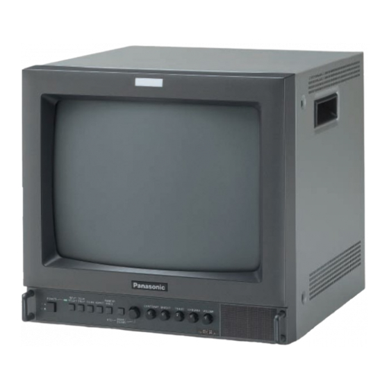
BT-S1315DA/BT-S1315DAD/BT-S1415DA/BT-S1415DAD
G19M-1 Chassis
Advertisement
Table of Contents

Related Manuals for Panasonic BT-S1315DA


Summary of Contents for Panasonic BT-S1315DA
-
Page 1: Table Of Contents
1.6 Repair Procedure of Horizontal Osc. Disable Circuit 2 Disassembly Instructions Color Video Monitor 2.1 Printed Circuit Board Layout 2.2 Removal of Top Cabinet BT-S1315DA/BT-S1315DAD/BT-S1415DA/BT-S1415DAD 2.3 Removal of Rear Cover G19M-1 Chassis 2.4 Removal of DS-P.C.Board (for BT-S1315DAD/S1415DAD only) 2.5 Removal of B- andW- P.C.Boards... - Page 2 bt_s1415.html 4.5 Notes 4.6 Switching between USER and FACTORY Modes 4.7 Purity Adjustment 4.7.1 Equipment to be used 4.7.2 Adjustment Procedure 4.8 Convergence Adjustment 4.8.1 Equipment to be used 4.8.2 Adjustment Procedure 4.9 Deflection Adjustment and Check 4.9.1 Equipment to be used 4.9.2 Initial Settings 4.9.3 Adjustment Procedure 4.10 Cut Off Adjustment...
- Page 3 bt_s1415.html 4.13.3 Preparations 4.13.4 6500K Adjustment 4.13.5 9300K Adjustment 4.14 SECAM Black Level Adjustment 4.14.1 Equipment to be used 4.14.2 Initial Settings 4.14.3 Adjustment Procedure 4.15 Brightness and ABL Adjustment 4.15.1 Equipment to be used 4.15.2 Initial Settings 4.15.3 Adjustment Procedure 4.16 Focus Adjustment 4.16.1 Equipment to be used 4.16.2 Initial Settings...
- Page 4 bt_s1415.html 5.4 No picture appears 5.5 No on-screen display appears 5.6 No sound comes out 6 Operating Instructions 7 Block Diagram 8 Schematic Diagram for Models BT- S1315DA/DAD and BT- S1415DA/DAD 9 Schematic Diagram 9.1 W-P.C.Board 9.2 A-P.C.Board(1/2) 9.3 A-P.C.Board(2/2) 9.4 B-P.C.Board(1/2) 9.5 B-P.C.Board(2/2) 10 Circuit Boards...
-
Page 5: Safety Precautions
file:///E:/BT-S1315DA_BT-S1315DAD_BT-S1415DA_BT-S1415DAD/SVC/s0100000000x.html 1 Safety Precautions TOP PREVIOUS NEXT 1.1 General Guidelines 1.2 Leakage Current Cold Check 1.3 Leakage Current Hot Check 1.4 X-Radiation 1.5 Horizontal Osc. Disable Circuit Test 1.6 Repair Procedure of Horizontal Osc. Disable Circuit •@ TOP PREVIOUS NEXT file:///E:/BT-S1315DA_BT-S1315DAD_BT-S1415DA_BT-S1415DAD/SVC/s0100000000x.html [2006-02-04 08:28:07]... -
Page 6: General Guidelines
file:///E:/BT-S1315DA_BT-S1315DAD_BT-S1415DA_BT-S1415DAD/SVC/s0101000000.html 1.1 General Guidelines TOP PREVIOUS NEXT It is advisable to insert an isolation transformer in the power line and AC supply before servicing a hot chassis. When servicing this monitor, observe the original lead dress, especially the lead dress in the high voltage circuits. -
Page 7: Leakage Current Cold Check
file:///E:/BT-S1315DA_BT-S1315DAD_BT-S1415DA_BT-S1415DAD/SVC/s0102000000.html 1.2 Leakage Current Cold Check TOP PREVIOUS NEXT 1. Unplug the AC power cord and connect a jumper wire between the two prongs of the AC plug. 2. Set the power switch of this monitor to the ON position. 3. -
Page 8: Leakage Current Hot Check
file:///E:/BT-S1315DA_BT-S1315DAD_BT-S1415DA_BT-S1415DAD/SVC/s0103000000.html 1.3 Leakage Current Hot Check TOP PREVIOUS NEXT 1. Plug the AC power cord directly into the AC outlet. Do not use an isolation transformer for this check. 2. Connect the test jig shown in Fig.1 between each exposed metallic part on the monitor and an earth ground such as a water pipe. - Page 9 file:///E:/BT-S1315DA_BT-S1315DAD_BT-S1415DA_BT-S1415DAD/SVC/s0103000000.html TOP PREVIOUS NEXT file:///E:/BT-S1315DA_BT-S1315DAD_BT-S1415DA_BT-S1415DAD/SVC/s0103000000.html (2 z 2) [2006-02-04 08:28:11]...
-
Page 10: X-Radiation
file:///E:/BT-S1315DA_BT-S1315DAD_BT-S1415DA_BT-S1415DAD/SVC/s0104000000.html 1.4 X-Radiation TOP PREVIOUS NEXT Warnings: The potential sources of X-Radiation in the monitor are the high voltage section and the picture tube. When using a picture tube test jig for service, check that the jig is capable of handling 28.5 kV without causing X-Radiation. -
Page 11: Horizontal Osc. Disable Circuit Test
This test must be made as a final check before the monitor is returned to the customer./Fig. 2 shows the horizontal osc. disable circuit. 1. With the rear cover removed, supply nominal 120 V AC for BT-S1315DA/DAD or 220 V AC for BT-S1415DA/DAD to the monitor and turn the power on. -
Page 12: Repair Procedure Of Horizontal
file:///E:/BT-S1315DA_BT-S1315DAD_BT-S1415DA_BT-S1415DAD/SVC/s0106000000.html 1.6 Repair Procedure of Horizontal Osc. Disable Circuit TOP PREVIOUS NEXT 1. Connect a DC voltmeter between the "+" side of C550 and a chassis ground. If the voltmeter does not read nearly 20 V, check R569, D520, C550, R571 and R573. 2. -
Page 13: Disassembly Instructions
file:///E:/BT-S1315DA_BT-S1315DAD_BT-S1415DA_BT-S1415DAD/SVC/s0200000000x.html 2 Disassembly Instructions TOP PREVIOUS NEXT Warnings: Be sure to unplug the AC power cord from the AC power outlet before disassembling this monitor. Cautions: When turning over a printed circuit board, be sure to put a insulating material under it to prevent a short circuit. - Page 14 file:///E:/BT-S1315DA_BT-S1315DAD_BT-S1415DA_BT-S1415DAD/SVC/s0200000000x.html TOP PREVIOUS NEXT file:///E:/BT-S1315DA_BT-S1315DAD_BT-S1415DA_BT-S1415DAD/SVC/s0200000000x.html (2 z 2) [2006-02-04 08:28:15]...
-
Page 15: Printed Circuit Board Layout
file:///E:/BT-S1315DA_BT-S1315DAD_BT-S1415DA_BT-S1415DAD/SVC/s0201000000.html 2.1 Printed Circuit Board Layout TOP PREVIOUS NEXT •@ TOP PREVIOUS NEXT file:///E:/BT-S1315DA_BT-S1315DAD_BT-S1415DA_BT-S1415DAD/SVC/s0201000000.html [2006-02-04 08:28:16]... -
Page 16: Removal Of Top Cabinet
file:///E:/BT-S1315DA_BT-S1315DAD_BT-S1415DA_BT-S1415DAD/SVC/s0202000000.html 2.2 Removal of Top Cabinet TOP PREVIOUS NEXT 1. Unscrew the 4 screws fixing the cabinet./(2 screws per side) 2. Unscrew the 6 screws fixing the cabinet. 3. After sliding the cabinet roughly 5 mm backward, lift it off while opening its bottom portions approx. - Page 17 file:///E:/BT-S1315DA_BT-S1315DAD_BT-S1415DA_BT-S1415DAD/SVC/s0202000000.html •@ TOP PREVIOUS NEXT file:///E:/BT-S1315DA_BT-S1315DAD_BT-S1415DA_BT-S1415DAD/SVC/s0202000000.html (2 z 2) [2006-02-04 08:28:17]...
-
Page 18: Removal Of Rear Cover
file:///E:/BT-S1315DA_BT-S1315DAD_BT-S1415DA_BT-S1415DAD/SVC/s0203000000.html 2.3 Removal of Rear Cover TOP PREVIOUS NEXT 1. Unscrew the 6 screws fixing the rear cover. 2. Remove the rear cover backward. •@ TOP PREVIOUS NEXT file:///E:/BT-S1315DA_BT-S1315DAD_BT-S1415DA_BT-S1415DAD/SVC/s0203000000.html [2006-02-04 08:28:18]... -
Page 19: Removal Of Ds-P.c.board
file:///E:/BT-S1315DA_BT-S1315DAD_BT-S1415DA_BT-S1415DAD/SVC/s0204000000.html 2.4 Removal of DS-P.C.Board (for BT- S1315DAD/S1415DAD only) TOP PREVIOUS NEXT 1. Remove the top cabinet according to the section 2.2."Removal of Top Cabinet". 2. Remove the rear cover according to the section 2.3. "Removal of Rear Cover". 3. Disconnect the wires connected from other P.C.Boards to DS-P.C.Board. 4. - Page 20 file:///E:/BT-S1315DA_BT-S1315DAD_BT-S1415DA_BT-S1415DAD/SVC/s0204000000.html •@ TOP PREVIOUS NEXT file:///E:/BT-S1315DA_BT-S1315DAD_BT-S1415DA_BT-S1415DAD/SVC/s0204000000.html (2 z 2) [2006-02-04 08:28:19]...
-
Page 21: Removal Of B- Andw- P.c.boards
file:///E:/BT-S1315DA_BT-S1315DAD_BT-S1415DA_BT-S1415DAD/SVC/s0205000000.html 2.5 Removal of B- and/W-P.C.Boards TOP PREVIOUS NEXT Note: If replacing B-P.C.Board with a new one, remove IC003 (EEPROM: TVRJ379) from the old P.C.Board and then install the removed IC on the new one. 1. Remove the top cabinet according to the section 2.2. "Removal of Top Cabinet". 2. - Page 22 file:///E:/BT-S1315DA_BT-S1315DAD_BT-S1415DA_BT-S1415DAD/SVC/s0205000000.html Note: 10. For BT-S1315DAD/S1415DAD, these screws are already removed when removing the SDI pack. 11. Disconnect the connectors between B-P.C.Board and W-P.C.Board. •@ TOP PREVIOUS NEXT file:///E:/BT-S1315DA_BT-S1315DAD_BT-S1415DA_BT-S1415DAD/SVC/s0205000000.html (2 z 2) [2006-02-04 08:28:20]...
-
Page 23: Removal Of A-P.c.board
file:///E:/BT-S1315DA_BT-S1315DAD_BT-S1415DA_BT-S1415DAD/SVC/s0206000000.html 2.6 Removal of A-P.C.Board TOP PREVIOUS NEXT 1. Remove the top cabinet according to the section 2.2. "Removal of Top Cabinet". 2. Remove the rear cover according to the section 2.3. "Removal of Rear Cover". 3. Disconnect the wires connected from other components to A- and B-P.C.Boards. 4. - Page 24 file:///E:/BT-S1315DA_BT-S1315DAD_BT-S1415DA_BT-S1415DAD/SVC/s0206000000.html 11. Unscrew the 7 screws fixing A-P.C.Board. 12. Unhook the hooks and remove the A-P.C.Board. •@ TOP PREVIOUS NEXT file:///E:/BT-S1315DA_BT-S1315DAD_BT-S1415DA_BT-S1415DAD/SVC/s0206000000.html (2 z 2) [2006-02-04 08:28:22]...
-
Page 25: Picture Tube Replacement
file:///E:/BT-S1315DA_BT-S1315DAD_BT-S1415DA_BT-S1415DAD/SVC/s0300000000x.html 3 Picture Tube Replacement TOP PREVIOUS NEXT Caution: Never mechanically stress the neck of the picture tube not to damage it. 3.1 Replacement Procedure 3.2 Location of Magnets •@ TOP PREVIOUS NEXT file:///E:/BT-S1315DA_BT-S1315DAD_BT-S1415DA_BT-S1415DAD/SVC/s0300000000x.html [2006-02-04 08:28:23]... -
Page 26: Replacement Procedure
file:///E:/BT-S1315DA_BT-S1315DAD_BT-S1415DA_BT-S1415DAD/SVC/s0301000000.html 3.1 Replacement Procedure TOP PREVIOUS NEXT Removal 1. Remove the plastic chassis block according to steps 1 to 4 inclusive in the section "Removal of A-P.C.Board". 2. Disconnect the CRT socket on the Y-P.C.Board. 3. Remove the anode cap from the picture tube. 4. -
Page 27: Location Of Magnets
file:///E:/BT-S1315DA_BT-S1315DAD_BT-S1415DA_BT-S1415DAD/SVC/s0302000000.html 3.2 Location of Magnets TOP PREVIOUS NEXT •@ TOP PREVIOUS NEXT file:///E:/BT-S1315DA_BT-S1315DAD_BT-S1415DA_BT-S1415DAD/SVC/s0302000000.html [2006-02-04 08:28:24]... -
Page 28: Measurements And Adjustments
file:///E:/BT-S1315DA_BT-S1315DAD_BT-S1415DA_BT-S1415DAD/SVC/s0400000000x.html 4 Measurements and Adjustments TOP PREVIOUS NEXT 4.1 Adjustment procedure Flowchart 4.2 Location of Test Points and Adjustment Control 4.3 Warnings 4.4 Caution 4.5 Notes 4.6 Switching between USER and FACTORY Modes 4.7 Purity Adjustment 4.7.1 Equipment to be used 4.7.2 Adjustment Procedure 4.8 Convergence Adjustment 4.8.1 Equipment to be used... - Page 29 file:///E:/BT-S1315DA_BT-S1315DAD_BT-S1415DA_BT-S1415DAD/SVC/s0400000000x.html 4.10.2 Initial Settings 4.10.3 Adjustment Procedure 4.11 Contrast Adjustment 4.11.1 Equipment to be used 4.11.2 Initial Settings 4.11.3 Adjustment Procedure 4.12 NTSC Color Output Adjustment 4.12.1 Equipment to be used 4.12.2 Initial Settings 4.12.3 Adjustment Procedure 4.13 White Balance Adjustment 4.13.1 Equipment to be used 4.13.2 Initial Setting 4.13.3 Preparations...
- Page 30 file:///E:/BT-S1315DA_BT-S1315DAD_BT-S1415DA_BT-S1415DAD/SVC/s0400000000x.html 4.15.1 Equipment to be used 4.15.2 Initial Settings 4.15.3 Adjustment Procedure 4.16 Focus Adjustment 4.16.1 Equipment to be used 4.16.2 Initial Settings 4.16.3 Adjustment Procedure 4.17 C/Y Output Adjustment (BT-S1315DAD/S1415DAD only) 4.17.1 Equipment to be used 4.17.2 Adjustment Procedure 4.18 X-radiation Protection Circuit Adjustment 4.18.1 Equipment to be used 4.18.2 Initial Settings...
-
Page 31: Adjustment Procedure Flowchart
file:///E:/BT-S1315DA_BT-S1315DAD_BT-S1415DA_BT-S1415DAD/SVC/s0401000000.html 4.1 Adjustment procedure Flowchart TOP PREVIOUS NEXT •@ TOP PREVIOUS NEXT file:///E:/BT-S1315DA_BT-S1315DAD_BT-S1415DA_BT-S1415DAD/SVC/s0401000000.html [2006-02-04 08:28:26]... -
Page 32: Location Of Test Points And Adjustment Control
file:///E:/BT-S1315DA_BT-S1315DAD_BT-S1415DA_BT-S1415DAD/SVC/s0402000000.html 4.2 Location of Test Points and Adjustment Control TOP PREVIOUS NEXT file:///E:/BT-S1315DA_BT-S1315DAD_BT-S1415DA_BT-S1415DAD/SVC/s0402000000.html (1 z 2) [2006-02-04 08:28:27]... - Page 33 file:///E:/BT-S1315DA_BT-S1315DAD_BT-S1415DA_BT-S1415DAD/SVC/s0402000000.html •@ TOP PREVIOUS NEXT file:///E:/BT-S1315DA_BT-S1315DAD_BT-S1415DA_BT-S1415DAD/SVC/s0402000000.html (2 z 2) [2006-02-04 08:28:27]...
-
Page 34: Warnings
file:///E:/BT-S1315DA_BT-S1315DAD_BT-S1415DA_BT-S1415DAD/SVC/s0403000000.html 4.3 Warnings TOP PREVIOUS NEXT Because this set has HOT and COLD sections in the power supply circuit, never touch the HOT and COLD sections at the same time to prevent you from getting an electric shock. Always unplug the AC power cord plug from the AC line outlet before disassembling the chassis. •@ TOP PREVIOUS NEXT file:///E:/BT-S1315DA_BT-S1315DAD_BT-S1415DA_BT-S1415DAD/SVC/s0403000000.html [2006-02-04 08:28:28]... -
Page 35: Caution
file:///E:/BT-S1315DA_BT-S1315DAD_BT-S1415DA_BT-S1415DAD/SVC/s0404000000.html 4.4 Caution TOP PREVIOUS NEXT Never short-circuit between the HOT and COLD sections to prevent damage to the components. Never measure the HOT and COLD sections at the same time when using any measurement instrument. When a screwdriver is needed during adjustment, use a nonmetallic screwdriver to prevent an unexpected short circuit. -
Page 36: Notes
This set needs a warm-up to stabilize each function, so operate the set to be adjusted over an hour before the adjustment. The AC power source voltage should be 120 V±2 V for BT-S1315DA/DAD or 220 V±2 V for BT- S1415DA/DAD, and its distortion less than 3%. -
Page 37: Switching Between User And Factory Modes
file:///E:/BT-S1315DA_BT-S1315DAD_BT-S1415DA_BT-S1415DAD/SVC/s0406000000.html 4.6 Switching between USER and FACTORY Modes TOP PREVIOUS NEXT USER Mode→ FACTORY Mode While pressing the SCAN switch, turn the Rotary switch 3 steps clockwise, then 1 step counterclockwise, then 3 steps clockwise, and then 1 step counterclockwise. FACTORY Mode→... -
Page 38: Purity Adjustment
file:///E:/BT-S1315DA_BT-S1315DAD_BT-S1415DA_BT-S1415DAD/SVC/s0407000000.html 4.7 Purity Adjustment TOP PREVIOUS NEXT 4.7.1 Equipment to be used 4.7.2 Adjustment Procedure •@ TOP PREVIOUS NEXT file:///E:/BT-S1315DA_BT-S1315DAD_BT-S1415DA_BT-S1415DAD/SVC/s0407000000.html [2006-02-04 08:28:33]... -
Page 39: Equipment To Be Used
file:///E:/BT-S1315DA_BT-S1315DAD_BT-S1415DA_BT-S1415DAD/SVC/s0407010000.html 4.7.1 Equipment to be used TOP PREVIOUS NEXT Degaussing Coil Microscope RGB Signal Generator: LINE B Digital Voltmeter: TPA1 (+) - TPA2 (-) •@ TOP PREVIOUS NEXT file:///E:/BT-S1315DA_BT-S1315DAD_BT-S1415DA_BT-S1415DAD/SVC/s0407010000.html [2006-02-04 08:28:34]... -
Page 40: Adjustment Procedure
file:///E:/BT-S1315DA_BT-S1315DAD_BT-S1415DA_BT-S1415DAD/SVC/s0407020000.html 4.7.2 Adjustment Procedure TOP PREVIOUS NEXT 1. Set the color temperature to "6500K". 2. Fully degauss the front, both sides, and top of the picture tube with an external degaussing coil. 3. Input a crosshatch pattern signal and adjust the convergence by horizontally and vertically positioning the static convergence magnet and deflection yoke. -
Page 41: Convergence Adjustment
file:///E:/BT-S1315DA_BT-S1315DAD_BT-S1415DA_BT-S1415DAD/SVC/s0408000000.html 4.8 Convergence Adjustment TOP PREVIOUS NEXT 4.8.1 Equipment to be used 4.8.2 Adjustment Procedure •@ TOP PREVIOUS NEXT file:///E:/BT-S1315DA_BT-S1315DAD_BT-S1415DA_BT-S1415DAD/SVC/s0408000000.html [2006-02-04 08:28:35]... -
Page 42: Equipment To Be Used
file:///E:/BT-S1315DA_BT-S1315DAD_BT-S1415DA_BT-S1415DAD/SVC/s0408010000.html 4.8.1 Equipment to be used TOP PREVIOUS NEXT RGB Signal Generator: LINE B •@ TOP PREVIOUS NEXT file:///E:/BT-S1315DA_BT-S1315DAD_BT-S1415DA_BT-S1415DAD/SVC/s0408010000.html [2006-02-04 08:28:36]... -
Page 43: Adjustment Procedure
file:///E:/BT-S1315DA_BT-S1315DAD_BT-S1415DA_BT-S1415DAD/SVC/s0408020000.html 4.8.2 Adjustment Procedure TOP PREVIOUS NEXT 1. Input a crosshatch pattern signal. 2. Adjust the 4-pole magnet to merge the blue lines with the red ones in the middle section of the screen. Note: 3. For the location of the magnets, refer to the chapter 3 Picture Tube Replacement. 4. -
Page 44: Deflection Adjustment And Check
file:///E:/BT-S1315DA_BT-S1315DAD_BT-S1415DA_BT-S1415DAD/SVC/s0409000000.html 4.9 Deflection Adjustment and Check TOP PREVIOUS NEXT 4.9.1 Equipment to be used 4.9.2 Initial Settings 4.9.3 Adjustment Procedure •@ TOP PREVIOUS NEXT file:///E:/BT-S1315DA_BT-S1315DAD_BT-S1415DA_BT-S1415DAD/SVC/s0409000000.html [2006-02-04 08:28:37]... -
Page 45: Equipment To Be Used
file:///E:/BT-S1315DA_BT-S1315DAD_BT-S1415DA_BT-S1415DAD/SVC/s0409010000.html 4.9.1 Equipment to be used TOP PREVIOUS NEXT NTSC Signal Generator: LINE A PAL Signal Generator: LINE A •@ TOP PREVIOUS NEXT file:///E:/BT-S1315DA_BT-S1315DAD_BT-S1415DA_BT-S1415DAD/SVC/s0409010000.html [2006-02-04 08:28:38]... -
Page 46: Initial Settings
file:///E:/BT-S1315DA_BT-S1315DAD_BT-S1415DA_BT-S1415DAD/SVC/s0409020000.html 4.9.2 Initial Settings TOP PREVIOUS NEXT BRIGHT, PHASE, CHROMA: center (click position) CONTRAST: maximum VOLUME (audio): minimum •@ TOP PREVIOUS NEXT file:///E:/BT-S1315DA_BT-S1315DAD_BT-S1415DA_BT-S1415DAD/SVC/s0409020000.html [2006-02-04 08:28:39]... -
Page 47: Adjustment Procedure
file:///E:/BT-S1315DA_BT-S1315DAD_BT-S1415DA_BT-S1415DAD/SVC/s0409030000.html 4.9.3 Adjustment Procedure TOP PREVIOUS NEXT 1. Input an NTSC monoscope pattern signal and check that the picture locks horizontally. 2. Set the SCAN switch to over-scanning mode (original size). 3. Set the monitor to the FACTORY mode and select DISPLAY REF from the menu. 4. -
Page 48: Cut Off Adjustment
file:///E:/BT-S1315DA_BT-S1315DAD_BT-S1415DA_BT-S1415DAD/SVC/s0410000000.html 4.10 Cut Off Adjustment TOP PREVIOUS NEXT 4.10.1 Equipment to be used 4.10.2 Initial Settings 4.10.3 Adjustment Procedure •@ TOP PREVIOUS NEXT file:///E:/BT-S1315DA_BT-S1315DAD_BT-S1415DA_BT-S1415DAD/SVC/s0410000000.html [2006-02-04 08:28:40]... -
Page 49: Equipment To Be Used
file:///E:/BT-S1315DA_BT-S1315DAD_BT-S1415DA_BT-S1415DAD/SVC/s0410010000.html 4.10.1 Equipment to be used TOP PREVIOUS NEXT NTSC Signal Generator: LINE A Oscilloscope: TPY4 (GK) - TPY7 (GND) •@ TOP PREVIOUS NEXT file:///E:/BT-S1315DA_BT-S1315DAD_BT-S1415DA_BT-S1415DAD/SVC/s0410010000.html [2006-02-04 08:28:41]... -
Page 50: Initial Settings
file:///E:/BT-S1315DA_BT-S1315DAD_BT-S1415DA_BT-S1415DAD/SVC/s0410020000.html 4.10.2 Initial Settings TOP PREVIOUS NEXT BRIGHT, PHASE, CHROMA: center (click position) CONTRAST: maximum VOLUME (audio): minimum •@ TOP PREVIOUS NEXT file:///E:/BT-S1315DA_BT-S1315DAD_BT-S1415DA_BT-S1415DAD/SVC/s0410020000.html [2006-02-04 08:28:42]... -
Page 51: Adjustment Procedure
file:///E:/BT-S1315DA_BT-S1315DAD_BT-S1415DA_BT-S1415DAD/SVC/s0410030000.html 4.10.3 Adjustment Procedure TOP PREVIOUS NEXT 1. Input a crosshatch pattern signal. 2. Set the SCREEN control to its minimum. 3. To display a horizontal single line, set the monitor to the FACTORY mode, then V COMPRESS on the menu to ON, and then select MENU OFF. 4. -
Page 52: Contrast Adjustment
file:///E:/BT-S1315DA_BT-S1315DAD_BT-S1415DA_BT-S1415DAD/SVC/s0411000000.html 4.11 Contrast Adjustment TOP PREVIOUS NEXT 4.11.1 Equipment to be used 4.11.2 Initial Settings 4.11.3 Adjustment Procedure •@ TOP PREVIOUS NEXT file:///E:/BT-S1315DA_BT-S1315DAD_BT-S1415DA_BT-S1415DAD/SVC/s0411000000.html [2006-02-04 08:28:43]... -
Page 53: Equipment To Be Used
file:///E:/BT-S1315DA_BT-S1315DAD_BT-S1415DA_BT-S1415DAD/SVC/s0411010000.html 4.11.1 Equipment to be used TOP PREVIOUS NEXT NTSC Signal Generator: LINE A RGB Signal Generator: LINE B Oscilloscope: TPY4 (GK) - TPY7 (GND) •@ TOP PREVIOUS NEXT file:///E:/BT-S1315DA_BT-S1315DAD_BT-S1415DA_BT-S1415DAD/SVC/s0411010000.html [2006-02-04 08:28:44]... -
Page 54: Initial Settings
file:///E:/BT-S1315DA_BT-S1315DAD_BT-S1415DA_BT-S1415DAD/SVC/s0411020000.html 4.11.2 Initial Settings TOP PREVIOUS NEXT BRIGHT, PHASE, CHROMA: center (click position) CONTRAST: maximum VOLUME (audio): minimum •@ TOP PREVIOUS NEXT file:///E:/BT-S1315DA_BT-S1315DAD_BT-S1415DA_BT-S1415DAD/SVC/s0411020000.html [2006-02-04 08:28:44]... -
Page 55: Adjustment Procedure
file:///E:/BT-S1315DA_BT-S1315DAD_BT-S1415DA_BT-S1415DAD/SVC/s0411030000.html 4.11.3 Adjustment Procedure TOP PREVIOUS NEXT 1. Input an NTSC crosshatch pattern signal and check that the black level is 140 V±5 V at TPY4 (GK). 2. Set the monitor to the FACTORY mode, then select PICTURE REF from the menu, and then adjust CONTRAST on the PICTURE REF menu to obtain B=60.0 V±1.0 V. -
Page 56: Ntsc Color Output
file:///E:/BT-S1315DA_BT-S1315DAD_BT-S1415DA_BT-S1415DAD/SVC/s0412000000.html 4.12 NTSC Color Output Adjustment TOP PREVIOUS NEXT 4.12.1 Equipment to be used 4.12.2 Initial Settings 4.12.3 Adjustment Procedure •@ TOP PREVIOUS NEXT file:///E:/BT-S1315DA_BT-S1315DAD_BT-S1415DA_BT-S1415DAD/SVC/s0412000000.html [2006-02-04 08:28:46]... -
Page 57: Equipment To Be Used
file:///E:/BT-S1315DA_BT-S1315DAD_BT-S1415DA_BT-S1415DAD/SVC/s0412010000.html 4.12.1 Equipment to be used TOP PREVIOUS NEXT NTSC Signal Generator: LINE A PAL Signal Generator: LINE A Oscilloscope: TPY6 (BK) - TPY7 (GND) •@ TOP PREVIOUS NEXT file:///E:/BT-S1315DA_BT-S1315DAD_BT-S1415DA_BT-S1415DAD/SVC/s0412010000.html [2006-02-04 08:28:46]... -
Page 58: Initial Settings
file:///E:/BT-S1315DA_BT-S1315DAD_BT-S1415DA_BT-S1415DAD/SVC/s0412020000.html 4.12.2 Initial Settings TOP PREVIOUS NEXT BRIGHT, PHASE, CHROMA: center (click position) CONTRAST: maximum VOLUME (audio): minimum •@ TOP PREVIOUS NEXT file:///E:/BT-S1315DA_BT-S1315DAD_BT-S1415DA_BT-S1415DAD/SVC/s0412020000.html [2006-02-04 08:28:47]... -
Page 59: Adjustment Procedure
file:///E:/BT-S1315DA_BT-S1315DAD_BT-S1415DA_BT-S1415DAD/SVC/s0412030000.html 4.12.3 Adjustment Procedure TOP PREVIOUS NEXT 1. Input an NTSC full field color bar signal. 2. Set the monitor to the FACTORY mode, then select PICTURE REF from the menu, and then adjust CHROMA and PHASE on the PICTURE REF menu to align the vertical positions of A, B, C, and D of the pulse below by using the doted lines as a guideline.At this time, adjust CHROMA for A and D and PHASE for B and C. -
Page 60: White Balance Adjustment
file:///E:/BT-S1315DA_BT-S1315DAD_BT-S1415DA_BT-S1415DAD/SVC/s0413000000.html 4.13 White Balance Adjustment TOP PREVIOUS NEXT 4.13.1 Equipment to be used 4.13.2 Initial Setting 4.13.3 Preparations 4.13.4 6500K Adjustment 4.13.5 9300K Adjustment •@ TOP PREVIOUS NEXT file:///E:/BT-S1315DA_BT-S1315DAD_BT-S1415DA_BT-S1415DAD/SVC/s0413000000.html [2006-02-04 08:28:48]... - Page 61 file:///E:/BT-S1315DA_BT-S1315DAD_BT-S1415DA_BT-S1415DAD/SVC/s0413010000.html 4.13.1 Equipment to be used TOP PREVIOUS NEXT NTSC Signal Generator: LINE A Color Analyzer Degaussing Coil •@ TOP PREVIOUS NEXT file:///E:/BT-S1315DA_BT-S1315DAD_BT-S1415DA_BT-S1415DAD/SVC/s0413010000.html [2006-02-04 08:28:49]...
-
Page 62: Initial Setting
file:///E:/BT-S1315DA_BT-S1315DAD_BT-S1415DA_BT-S1415DAD/SVC/s0413020000.html 4.13.2 Initial Setting TOP PREVIOUS NEXT CHROMA: center (click position) •@ TOP PREVIOUS NEXT file:///E:/BT-S1315DA_BT-S1315DAD_BT-S1415DA_BT-S1415DAD/SVC/s0413020000.html [2006-02-04 08:28:50]... -
Page 63: Preparations
file:///E:/BT-S1315DA_BT-S1315DAD_BT-S1415DA_BT-S1415DAD/SVC/s0413030000.html 4.13.3 Preparations TOP PREVIOUS NEXT 1. Input a window pattern signal. 2. Fully degauss the front, both sides, and top of the picture tube with an external degaussing coil. 3. Attach the light receiving element of a color analyzer to the front of the picture tube. Note: 4. -
Page 64: 6500K Adjustment
file:///E:/BT-S1315DA_BT-S1315DAD_BT-S1415DA_BT-S1415DAD/SVC/s0413040000.html 4.13.4 6500K Adjustment TOP PREVIOUS NEXT 1. Set the monitor to the FACTORY mode and then COLOR TEMP on the menu to 6500K. 2. Adjust the input signal to obtain a brightness of Y=5 nit±1.5 nit. 3. Adjust R-BIAS and B-BIAS to obtain a color temperature of x=313±3 and y=329±3. 4. -
Page 65: 9300K Adjustment
file:///E:/BT-S1315DA_BT-S1315DAD_BT-S1415DA_BT-S1415DAD/SVC/s0413050000.html 4.13.5 9300K Adjustment TOP PREVIOUS NEXT 1. Set the monitor to the FACTORY mode and then COLOR TEMP on the menu to 9300K. 2. Adjust this item in a procedure similar to step 4 to obtain a color temperature of x=281±3 and y=301±3. -
Page 66: Secam Black Level Adjustment
file:///E:/BT-S1315DA_BT-S1315DAD_BT-S1415DA_BT-S1415DAD/SVC/s0414000000.html 4.14 SECAM Black Level Adjustment TOP PREVIOUS NEXT 4.14.1 Equipment to be used 4.14.2 Initial Settings 4.14.3 Adjustment Procedure •@ TOP PREVIOUS NEXT file:///E:/BT-S1315DA_BT-S1315DAD_BT-S1415DA_BT-S1415DAD/SVC/s0414000000.html [2006-02-04 08:28:52]... -
Page 67: Equipment To Be Used
file:///E:/BT-S1315DA_BT-S1315DAD_BT-S1415DA_BT-S1415DAD/SVC/s0414010000.html 4.14.1 Equipment to be used TOP PREVIOUS NEXT SECAM Signal Generator: LINE A Oscilloscope: TPB19 (B-Y) - TPB35 (GND) , TPB20 (R-Y) - TPB35 (GND) •@ TOP PREVIOUS NEXT file:///E:/BT-S1315DA_BT-S1315DAD_BT-S1415DA_BT-S1415DAD/SVC/s0414010000.html [2006-02-04 08:28:53]... -
Page 68: Initial Settings
file:///E:/BT-S1315DA_BT-S1315DAD_BT-S1415DA_BT-S1415DAD/SVC/s0414020000.html 4.14.2 Initial Settings TOP PREVIOUS NEXT BRIGHT, PHASE, CHROMA: center (click position) CONTRAST: maximum VOLUME (audio): minimum •@ TOP PREVIOUS NEXT file:///E:/BT-S1315DA_BT-S1315DAD_BT-S1415DA_BT-S1415DAD/SVC/s0414020000.html [2006-02-04 08:28:54]... -
Page 69: Adjustment Procedure
file:///E:/BT-S1315DA_BT-S1315DAD_BT-S1415DA_BT-S1415DAD/SVC/s0414030000.html 4.14.3 Adjustment Procedure TOP PREVIOUS NEXT 1. Input a SECAM color bar signal. 2. Connect an oscilloscope to TPB19 (B-Y). 3. Set the monitor to the FACTORY mode, then select PICTURE REF from the menu, and then adjust SECAM B-Y OUT on the PICTURE REF menu to level the color signal periods with the H blanking ones. -
Page 70: Brightness And Abl Adjustment
file:///E:/BT-S1315DA_BT-S1315DAD_BT-S1415DA_BT-S1415DAD/SVC/s0415000000.html 4.15 Brightness and ABL Adjustment TOP PREVIOUS NEXT 4.15.1 Equipment to be used 4.15.2 Initial Settings 4.15.3 Adjustment Procedure •@ TOP PREVIOUS NEXT file:///E:/BT-S1315DA_BT-S1315DAD_BT-S1415DA_BT-S1415DAD/SVC/s0415000000.html [2006-02-04 08:28:56]... -
Page 71: Equipment To Be Used
file:///E:/BT-S1315DA_BT-S1315DAD_BT-S1415DA_BT-S1415DAD/SVC/s0415010000.html 4.15.1 Equipment to be used TOP PREVIOUS NEXT NTSC Signal Generator: LINE A Digital Voltmeter: TPA1 (+) - TPA2 (-) •@ TOP PREVIOUS NEXT file:///E:/BT-S1315DA_BT-S1315DAD_BT-S1415DA_BT-S1415DAD/SVC/s0415010000.html [2006-02-04 08:28:57]... -
Page 72: Initial Settings
file:///E:/BT-S1315DA_BT-S1315DAD_BT-S1415DA_BT-S1415DAD/SVC/s0415020000.html 4.15.2 Initial Settings TOP PREVIOUS NEXT BRIGHT, PHASE, CHROMA: center (click position) CONTRAST: maximum VOLUME (audio): minimum •@ TOP PREVIOUS NEXT file:///E:/BT-S1315DA_BT-S1315DAD_BT-S1415DA_BT-S1415DAD/SVC/s0415020000.html [2006-02-04 08:28:57]... -
Page 73: Adjustment Procedure
file:///E:/BT-S1315DA_BT-S1315DAD_BT-S1415DA_BT-S1415DAD/SVC/s0415030000.html 4.15.3 Adjustment Procedure TOP PREVIOUS NEXT 1. Input an SMPTE color bar signal. 2. Set the monitor to the FACTORY mode, then select PICTURE REF from the menu, and then adjust BRIGHT on the PICTURE REF menu to set the black level to the point that the B portion just starts to go down. -
Page 74: Focus Adjustment
file:///E:/BT-S1315DA_BT-S1315DAD_BT-S1415DA_BT-S1415DAD/SVC/s0416000000.html 4.16 Focus Adjustment TOP PREVIOUS NEXT 4.16.1 Equipment to be used 4.16.2 Initial Settings 4.16.3 Adjustment Procedure •@ TOP PREVIOUS NEXT file:///E:/BT-S1315DA_BT-S1315DAD_BT-S1415DA_BT-S1415DAD/SVC/s0416000000.html [2006-02-04 08:28:59]... -
Page 75: Equipment To Be Used
file:///E:/BT-S1315DA_BT-S1315DAD_BT-S1415DA_BT-S1415DAD/SVC/s0416010000.html 4.16.1 Equipment to be used TOP PREVIOUS NEXT NTSC Signal Generator: LINE A •@ TOP PREVIOUS NEXT file:///E:/BT-S1315DA_BT-S1315DAD_BT-S1415DA_BT-S1415DAD/SVC/s0416010000.html [2006-02-04 08:29:00]... -
Page 76: Initial Settings
file:///E:/BT-S1315DA_BT-S1315DAD_BT-S1415DA_BT-S1415DAD/SVC/s0416020000.html 4.16.2 Initial Settings TOP PREVIOUS NEXT BRIGHT, PHASE, CHROMA: center (click position) CONTRAST: maximum VOLUME (audio): minimum •@ TOP PREVIOUS NEXT file:///E:/BT-S1315DA_BT-S1315DAD_BT-S1415DA_BT-S1415DAD/SVC/s0416020000.html [2006-02-04 08:29:00]... -
Page 77: Adjustment Procedure
file:///E:/BT-S1315DA_BT-S1315DAD_BT-S1415DA_BT-S1415DAD/SVC/s0416030000.html 4.16.3 Adjustment Procedure TOP PREVIOUS NEXT 1. Input a monoscope pattern signal. 2. Adjust the FOCUS control to obtain correct focus in the middle and periphery of the screen. •@ TOP PREVIOUS NEXT file:///E:/BT-S1315DA_BT-S1315DAD_BT-S1415DA_BT-S1415DAD/SVC/s0416030000.html [2006-02-04 08:29:01]... - Page 78 file:///E:/BT-S1315DA_BT-S1315DAD_BT-S1415DA_BT-S1415DAD/SVC/s0417000000.html 4.17 C/Y Output Adjustment (BT- S1315DAD/S1415DAD only) TOP PREVIOUS NEXT 4.17.1 Equipment to be used 4.17.2 Adjustment Procedure •@ TOP PREVIOUS NEXT file:///E:/BT-S1315DA_BT-S1315DAD_BT-S1415DA_BT-S1415DAD/SVC/s0417000000.html [2006-02-04 08:29:02]...
-
Page 79: Equipment To Be Used
file:///E:/BT-S1315DA_BT-S1315DAD_BT-S1415DA_BT-S1415DAD/SVC/s0417010000.html 4.17.1 Equipment to be used TOP PREVIOUS NEXT SMPTE259M Signal Generator: SDI Oscilloscope: TP8 (PB OUT) - TP5 (GND) , TP9 (PR OUT) - TP5 (GND) , TP7 (Y OUT) - TP5 (GND) •@ TOP PREVIOUS NEXT file:///E:/BT-S1315DA_BT-S1315DAD_BT-S1415DA_BT-S1415DAD/SVC/s0417010000.html [2006-02-04 08:29:04]... -
Page 80: Adjustment Procedure
file:///E:/BT-S1315DA_BT-S1315DAD_BT-S1415DA_BT-S1415DAD/SVC/s0417020000.html 4.17.2 Adjustment Procedure TOP PREVIOUS NEXT 1. Input an SMPTE259M 100% color bar signal. 2. Adjust R4143 and R4146 to obtain the waveform is as the figure below. 3. Adjust R4144 to obtain the waveform is as the figure below. 4. -
Page 81: X-Radiation Protection Circuit Adjustment
file:///E:/BT-S1315DA_BT-S1315DAD_BT-S1415DA_BT-S1415DAD/SVC/s0418000000.html 4.18 X-radiation Protection Circuit Adjustment TOP PREVIOUS NEXT 4.18.1 Equipment to be used 4.18.2 Initial Settings 4.18.3 Adjustment Procedure •@ TOP PREVIOUS NEXT file:///E:/BT-S1315DA_BT-S1315DAD_BT-S1415DA_BT-S1415DAD/SVC/s0418000000.html [2006-02-04 08:29:06]... -
Page 82: Equipment To Be Used
file:///E:/BT-S1315DA_BT-S1315DAD_BT-S1415DA_BT-S1415DAD/SVC/s0418010000.html 4.18.1 Equipment to be used TOP PREVIOUS NEXT PAL Signal Generator: LINE A High-voltage Meter (Electrostatic type): picture tube anode-COLD GND Digital Voltmeter: TPA1 (+) - TPA2 (-) DC Power Supply (100 V -150 V): TPA6 (+) - TPA4 (-) 56 kΩ... -
Page 83: Initial Settings
file:///E:/BT-S1315DA_BT-S1315DAD_BT-S1415DA_BT-S1415DAD/SVC/s0418020000.html 4.18.2 Initial Settings TOP PREVIOUS NEXT BRIGHT, PHASE, CHROMA: center (click position) CONTRAST: maximum VOLUME (audio): minimum H SIZE, SCREEN control: correctly adjusted condition. •@ TOP PREVIOUS NEXT file:///E:/BT-S1315DA_BT-S1315DAD_BT-S1415DA_BT-S1415DAD/SVC/s0418020000.html [2006-02-04 08:29:08]... -
Page 84: Adjustment Procedure
file:///E:/BT-S1315DA_BT-S1315DAD_BT-S1415DA_BT-S1415DAD/SVC/s0418030000.html 4.18.3 Adjustment Procedure TOP PREVIOUS NEXT 1. Input a PAL black level signal. 2. Connect DC power supply (100 V - 150 V) and electronic dummy load (150 mA) as shown below. 3. Turn on the monitor. 4. Set the SCAN switch to over-scanning mode (original size). 5. - Page 85 file:///E:/BT-S1315DA_BT-S1315DAD_BT-S1415DA_BT-S1415DAD/SVC/s0418030000.html 12. Minimize the DC power supply voltage gradually and turn it off. 13. Turn off the monitor. 14. Connect 56 kΩ / 5 W resistor as shown below. 15. Disconnect the resistor, DC power supply and electoronic dummy load. 16.
-
Page 86: Troubleshooting
file:///E:/BT-S1315DA_BT-S1315DAD_BT-S1415DA_BT-S1415DAD/SVC/s0500000000x.html 5 Troubleshooting TOP PREVIOUS NEXT 5.1 The power is not turned on 5.2 No raster appears 5.3 The raster is a horizontal 5.4 No picture appears 5.5 No on-screen display appears 5.6 No sound comes out •@ TOP PREVIOUS NEXT file:///E:/BT-S1315DA_BT-S1315DAD_BT-S1415DA_BT-S1415DAD/SVC/s0500000000x.html [2006-02-04 08:29:10]... -
Page 87: The Power Is Not Turned On
file:///E:/BT-S1315DA_BT-S1315DAD_BT-S1415DA_BT-S1415DAD/SVC/s0501000000.html 5.1 The power is not turned on TOP PREVIOUS NEXT •@ file:///E:/BT-S1315DA_BT-S1315DAD_BT-S1415DA_BT-S1415DAD/SVC/s0501000000.html (1 z 2) [2006-02-04 08:29:11]... - Page 88 file:///E:/BT-S1315DA_BT-S1315DAD_BT-S1415DA_BT-S1415DAD/SVC/s0501000000.html TOP PREVIOUS NEXT file:///E:/BT-S1315DA_BT-S1315DAD_BT-S1415DA_BT-S1415DAD/SVC/s0501000000.html (2 z 2) [2006-02-04 08:29:11]...
-
Page 89: No Raster Appears
file:///E:/BT-S1315DA_BT-S1315DAD_BT-S1415DA_BT-S1415DAD/SVC/s0502000000.html 5.2 No raster appears TOP PREVIOUS NEXT •@ TOP PREVIOUS NEXT file:///E:/BT-S1315DA_BT-S1315DAD_BT-S1415DA_BT-S1415DAD/SVC/s0502000000.html [2006-02-04 08:29:12]... -
Page 90: The Raster Is A Horizontal
file:///E:/BT-S1315DA_BT-S1315DAD_BT-S1415DA_BT-S1415DAD/SVC/s0503000000.html 5.3 The raster is a horizontal TOP PREVIOUS NEXT •@ TOP PREVIOUS NEXT file:///E:/BT-S1315DA_BT-S1315DAD_BT-S1415DA_BT-S1415DAD/SVC/s0503000000.html [2006-02-04 08:29:13]... -
Page 91: No Picture Appears
file:///E:/BT-S1315DA_BT-S1315DAD_BT-S1415DA_BT-S1415DAD/SVC/s0504000000.html 5.4 No picture appears TOP PREVIOUS NEXT file:///E:/BT-S1315DA_BT-S1315DAD_BT-S1415DA_BT-S1415DAD/SVC/s0504000000.html (1 z 2) [2006-02-04 08:29:14]... - Page 92 file:///E:/BT-S1315DA_BT-S1315DAD_BT-S1415DA_BT-S1415DAD/SVC/s0504000000.html •@ TOP PREVIOUS NEXT file:///E:/BT-S1315DA_BT-S1315DAD_BT-S1415DA_BT-S1415DAD/SVC/s0504000000.html (2 z 2) [2006-02-04 08:29:14]...
-
Page 93: No On-Screen Display Appears
file:///E:/BT-S1315DA_BT-S1315DAD_BT-S1415DA_BT-S1415DAD/SVC/s0505000000.html 5.5 No on-screen display appears TOP PREVIOUS NEXT •@ TOP PREVIOUS NEXT file:///E:/BT-S1315DA_BT-S1315DAD_BT-S1415DA_BT-S1415DAD/SVC/s0505000000.html [2006-02-04 08:29:14]... -
Page 94: No Sound Comes Out
file:///E:/BT-S1315DA_BT-S1315DAD_BT-S1415DA_BT-S1415DAD/SVC/s0506000000.html 5.6 No sound comes out TOP PREVIOUS NEXT •@ TOP PREVIOUS NEXT file:///E:/BT-S1315DA_BT-S1315DAD_BT-S1415DA_BT-S1415DAD/SVC/s0506000000.html [2006-02-04 08:29:15]... -
Page 95: Operating Instructions
For models BT-S1315DAD/BT-S1315DA, please read this chapter to translate the model number as below. BT-S1415DAD - BT-S1315DAD BT-S1415DA - BT-S1315DA •@... -
Page 96: Block Diagram
file:///E:/BT-S1315DA_BT-S1315DAD_BT-S1415DA_BT-S1415DAD/SVC/s0700000000x.html 7 Block Diagram TOP PREVIOUS NEXT •@ TOP PREVIOUS NEXT file:///E:/BT-S1315DA_BT-S1315DAD_BT-S1415DA_BT-S1415DAD/SVC/s0700000000x.html [2006-02-04 08:29:28]... - Page 97 8 Schematic Diagram for Models BT-S1315DA/DAD and BT-S1415DA/DAD TOP PREVIOUS NEXT file:///E:/BT-S1315DA_BT-S1315DAD_BT-S1415DA_BT-S1415DAD/SVC/s0800000000x.html (1 z 2) [2006-02-04 08:29:32]...
- Page 98 file:///E:/BT-S1315DA_BT-S1315DAD_BT-S1415DA_BT-S1415DAD/SVC/s0800000000x.html •@ TOP PREVIOUS NEXT file:///E:/BT-S1315DA_BT-S1315DAD_BT-S1415DA_BT-S1415DAD/SVC/s0800000000x.html (2 z 2) [2006-02-04 08:29:32]...
-
Page 99: Schematic Diagram
file:///E:/BT-S1315DA_BT-S1315DAD_BT-S1415DA_BT-S1415DAD/SVC/s0900000000x.html 9 Schematic Diagram TOP PREVIOUS NEXT 9.1 W-P.C.Board 9.2 A-P.C.Board(1/2) 9.3 A-P.C.Board(2/2) 9.4 B-P.C.Board(1/2) 9.5 B-P.C.Board(2/2) •@ TOP PREVIOUS NEXT file:///E:/BT-S1315DA_BT-S1315DAD_BT-S1415DA_BT-S1415DAD/SVC/s0900000000x.html [2006-02-04 08:29:37]... -
Page 100: W-P.c.board
file:///E:/BT-S1315DA_BT-S1315DAD_BT-S1415DA_BT-S1415DAD/SVC/s0901000000.html 9.1 W-P.C.Board TOP PREVIOUS NEXT •@ TOP PREVIOUS NEXT file:///E:/BT-S1315DA_BT-S1315DAD_BT-S1415DA_BT-S1415DAD/SVC/s0901000000.html [2006-02-04 08:29:43]... -
Page 101: A-P.c.board(1&Sol;2)
file:///E:/BT-S1315DA_BT-S1315DAD_BT-S1415DA_BT-S1415DAD/SVC/s0902000000.html 9.2 A-P.C.Board(1/2) TOP PREVIOUS NEXT •@ TOP PREVIOUS NEXT file:///E:/BT-S1315DA_BT-S1315DAD_BT-S1415DA_BT-S1415DAD/SVC/s0902000000.html [2006-02-04 08:29:59]... -
Page 102: A-P.c.board(2&Sol;2)
file:///E:/BT-S1315DA_BT-S1315DAD_BT-S1415DA_BT-S1415DAD/SVC/s0903000000.html 9.3 A-P.C.Board(2/2) TOP PREVIOUS NEXT •@ TOP PREVIOUS NEXT file:///E:/BT-S1315DA_BT-S1315DAD_BT-S1415DA_BT-S1415DAD/SVC/s0903000000.html [2006-02-04 08:30:03]... -
Page 103: B-P.c.board(1&Sol;2)
file:///E:/BT-S1315DA_BT-S1315DAD_BT-S1415DA_BT-S1415DAD/SVC/s0904000000.html 9.4 B-P.C.Board(1/2) TOP PREVIOUS NEXT •@ TOP PREVIOUS NEXT file:///E:/BT-S1315DA_BT-S1315DAD_BT-S1415DA_BT-S1415DAD/SVC/s0904000000.html [2006-02-04 08:30:07]... -
Page 104: B-P.c.board(2&Sol;2)
file:///E:/BT-S1315DA_BT-S1315DAD_BT-S1415DA_BT-S1415DAD/SVC/s0905000000.html 9.5 B-P.C.Board(2/2) TOP PREVIOUS NEXT •@ TOP PREVIOUS NEXT file:///E:/BT-S1315DA_BT-S1315DAD_BT-S1415DA_BT-S1415DAD/SVC/s0905000000.html [2006-02-04 08:30:14]... -
Page 105: Circuit Boards
file:///E:/BT-S1315DA_BT-S1315DAD_BT-S1415DA_BT-S1415DAD/SVC/s1000000000x.html 10 Circuit Boards TOP PREVIOUS NEXT 10.1 A-P.C.Board 10.2 B-P.C.Board/ W-P.C.Board(Foil Side) 10.3 B-P.C.Board (Component Side) Y/S/T/N/ Board(Foil Side) •@ TOP PREVIOUS NEXT file:///E:/BT-S1315DA_BT-S1315DAD_BT-S1415DA_BT-S1415DAD/SVC/s1000000000x.html [2006-02-04 08:30:17]... -
Page 106: A-P.c.board
file:///E:/BT-S1315DA_BT-S1315DAD_BT-S1415DA_BT-S1415DAD/SVC/s1001000000.html 10.1 A-P.C.Board TOP PREVIOUS NEXT •@ TOP PREVIOUS NEXT file:///E:/BT-S1315DA_BT-S1315DAD_BT-S1415DA_BT-S1415DAD/SVC/s1001000000.html [2006-02-04 08:30:18]... - Page 107 file:///E:/BT-S1315DA_BT-S1315DAD_BT-S1415DA_BT-S1415DAD/SVC/s1002000000.html 10.2 B-P.C.Board/ W-P.C.Board(Foil Side) TOP PREVIOUS NEXT •@ TOP PREVIOUS NEXT file:///E:/BT-S1315DA_BT-S1315DAD_BT-S1415DA_BT-S1415DAD/SVC/s1002000000.html [2006-02-04 08:30:24]...
-
Page 108: B-P.c.board (Component Side)
file:///E:/BT-S1315DA_BT-S1315DAD_BT-S1415DA_BT-S1415DAD/SVC/s1003000000.html 10.3 B-P.C.Board (Component Side) Y/S/T/N/ Board(Foil Side) TOP PREVIOUS NEXT •@ TOP PREVIOUS NEXT file:///E:/BT-S1315DA_BT-S1315DAD_BT-S1415DA_BT-S1415DAD/SVC/s1003000000.html [2006-02-04 08:30:32]... -
Page 109: Exproded Views Pv
file:///E:/BT-S1315DA_BT-S1315DAD_BT-S1415DA_BT-S1415DAD/SVC/s1100000000e.html 11 Exproded Views TOP PREVIOUS NEXT •@ TOP PREVIOUS NEXT file:///E:/BT-S1315DA_BT-S1315DAD_BT-S1415DA_BT-S1415DAD/SVC/s1100000000e.html [2006-02-04 08:30:36]... -
Page 110: Replacement Parts List
file:///E:/BT-S1315DA_BT-S1315DAD_BT-S1415DA_BT-S1415DAD/SVC/s1200000000x.html 12 Replacement Parts List TOP PREVIOUS Ref. No. Part No. Part Name& Description Remarks MECHANICAL PARTS A34JCD91X PICTURE TUBE KDY3GJB55F DEFLECTION YOKE TLC2042-1 CONVERGENCE YOKE EAS7D09A SPEAKER TXFKA01NERZ TOP CABINET ASSY S1415DAD,S1415DA TXFKA01NESZ TOP CABINET ASSY S1315DAD,S1315DA TKK69279-5 HANDEL TKRA20001 ANGLE TKUX04401... - Page 111 file:///E:/BT-S1315DA_BT-S1315DAD_BT-S1415DA_BT-S1415DAD/SVC/s1200000000x.html TBMD861 MODEL NAME PLATE S1415DAD TBMD908 MODEL NAME PLATE S1415DA TBMD950 MODEL NAME PLATE S1315DAD TBMD951 MODEL NAME PLATE S1315DA TBMU094 TERMINAL PLATE S1415DAD,S1315DAD TBMU103 TERMINAL PLATE S1415DA,S1315DA TES1208 SPRING THT1064 CRT SCREW TJS118070 AC INLET TJS8A4370 BNC TERMINAL S1415DAD,S1315DAD TMM15404-1 SPACER RING...
- Page 112 file:///E:/BT-S1315DA_BT-S1315DAD_BT-S1415DA_BT-S1415DAD/SVC/s1200000000x.html XYA4+EF8 SCREW XYA4+EJ12FZ SCREW XYE3+EF6FZ SCREW S1415DAD,S1315DAD XYN3+F10 SCREW XYN3+F12 SCREW XYN3+F6 SCREW INTEGATED CIRCUITS IC001 C2CBHF000131 IC002 MB90096-129 MOS IC (MICOM LSI) IC003 TVRJ379 IC004 MN1280R MOS IC (MICON LSI) IC201 AN5265 LINEAR IC IC351 TDA6103Q-N3 IC400 TA8859AP LINEAR IC IC401 LA7832...
- Page 113 file:///E:/BT-S1315DA_BT-S1315DAD_BT-S1415DA_BT-S1415DAD/SVC/s1200000000x.html Q301 2SB710A TRANSISTOR Q401,02 2SD601AR TRANSISTOR Q409 2SD601AR TRANSISTOR Q412,13 2SD601AR TRANSISTOR Q512 2SD1266APLB TRANSISTOR Q513 2SA1309A TRANSISTOR Q514 2SD601AR TRANSISTOR Q515 2SB709A TRANSISTOR Q517 2SD601AR TRANSISTOR Q518 2SB709A TRANSISTOR Q520 2SD601AR TRANSISTOR Q521 2SB709A TRANSISTOR Q551 2SC3940A TRANSISTOR Q552 2SD2499 TRANSISTOR...
- Page 114 file:///E:/BT-S1315DA_BT-S1315DAD_BT-S1415DA_BT-S1415DAD/SVC/s1200000000x.html Q3022,23 2SD601AR TRANSISTOR Q3102-05 2SD601AR TRANSISTOR S1415DAD,S1315DAD Q3106 2SB710A TRANSISTOR S1415DAD,S1315DAD Q3206 2SD601AR TRANSISTOR Q6501 2SD601AR TRANSISTOR Q6502 2SB709A TRANSISTOR Q6503 2SD601A TRANSISTOR DIODES D001 LN31GPH LED (GREEN) D012 MA152K DIODE D302,03 MA152K DIODE D304-06 MA165 DIODE D310 MA4068L ZENER DIODE D357 MA4150...
- Page 115 file:///E:/BT-S1315DA_BT-S1315DAD_BT-S1415DA_BT-S1415DAD/SVC/s1200000000x.html D526 MA152K DIODE D527 AS01A DIODE D541 MA4270H ZENER DIODE D556 MA182 DIODE D600 MA3082L ZENER DIODE D601,02 MA4068M ZENER DIODE D603 MA4091M ZENER DIODE D605 MA152K DIODE D801 ERZV14D821 VARISTOR S1415DAD,S1415DA D802 D4SB80Z DIODE D807 ERA15-04 DIODE D811 TMPG10G3 DIODE D812-14...
- Page 116 file:///E:/BT-S1315DA_BT-S1315DAD_BT-S1415DA_BT-S1415DAD/SVC/s1200000000x.html D842 MA165 DIODE D850 TVSRU3N DIODE D851 MA165 DIODE D1001-04 LN81RPH LED (ORANGE) D3001-08 MA152K DIODE D3102-06 MA152K DIODE S1415DAD,S1315DAD D3107 MA152K DIODE COILS L201 ELEIE470KA PEAKING COIL L402 TLT101J991K PEAKING COIL L501 ELH5L7122 LINEARITY COIL L503 ELC16B821L CHOKE COIL L552 ELEIE682KA CHOKE COIL...
- Page 117 file:///E:/BT-S1315DA_BT-S1315DAD_BT-S1415DA_BT-S1415DAD/SVC/s1200000000x.html T802 ETS33AC4B6NC SWITCHING TRANS RESISTORS R001-03 ERJ6GEYJ103 M 10KOHM,J,1/10W R004 ERJ6GEYJ473 M 47KOHM,J,1/10W R008,09 ERJ6GEYJ103 M 10KOHM,J,1/10W R011 ERJ6GEY0R00 M 0 OHM,J,1/10W R012-15 ERJ6GEYJ101 M 100 OHM,J,1/10W R016 ERJ6GEYJ470 M 47 OHM,J,1/10W R017 ERJ6GEYJ101 M 100 OHM,J,1/10W R018 ERJ6GEYJ103 M 10KOHM,J,1/10W R019 ERJ6GEYJ333...
- Page 118 file:///E:/BT-S1315DA_BT-S1315DAD_BT-S1415DA_BT-S1415DAD/SVC/s1200000000x.html R080-82 ERJ6GEYJ472 M 4.7KOHM,J,1/10W R083 ERJ6GEYJ123 M 12KOHM,J,1/10W R084 ERJ6GEYJ472 M 4.7KOHM,J,1/10W R085,86 ERJ6GEYJ123 M 12KOHM,J,1/10W R088,89 ERJ6GEYJ472 M 4.7KOHM,J,1/10W R090 ERJ6GEYJ471 M 470 OHM,J,1/10W R091 ERJ6GEYJ103 M 10KOHM,J,1/10W R092 ERJ6GEYJ223 M 22KOHM,J,1/10W R093,94 ERJ6GEYJ151 M 150 OHM,J,1/10W R095-101 ERJ6GEYJ473 M 47KOHM,J,1/10W R103...
- Page 119 file:///E:/BT-S1315DA_BT-S1315DAD_BT-S1415DA_BT-S1415DAD/SVC/s1200000000x.html R214 ERQ2CJP120S F 12 OHM, J, 2W R215 ERJ6GEYJ103 M 10KOHM,J,1/10W R220 ERJ6GEYJ332 M 3.3KOHM,J,1/10W R221 ERJ6GEYJ101 M 100 OHM,J,1/10W R302 ERDS2TJ101 C 100 OHM, J,1/4W R303 ERJ6GEYJ223 M 22KOHM,J,1/10W R351-53 ERJ6GEYJ222 M 2.2KOHM,J,1/10W R354 ERJ6ENF3301 M 3.3KOHM, 1/10W R355 ERJ6GEYJ562 M 5.6KOHM,J,1/10W...
- Page 120 file:///E:/BT-S1315DA_BT-S1315DAD_BT-S1415DA_BT-S1415DAD/SVC/s1200000000x.html R437 ERJ6GEYJ102 M 1KOHM,J,1/10W R438,39 ERDS2TJ471 C 470 OHM, J,1/4W R444 ERDS2TJ222 C 2.2KOHM, J,1/4W R445 ERDS2TJ103 C 10KOHM, J,1/4W R446 ERDS2TJ223 C 22KOHM, J,1/4W R448 ERDS2TJ103 C 10KOHM, J,1/4W R449 ERDS2TJ563 C 56KOHM, J,1/4W R450 ERDS1FJ1R5 C 1.5 OHM, J,1/2W R453 ERDS2TJ394 C 390KOHM, J,1/4W...
- Page 121 file:///E:/BT-S1315DA_BT-S1315DAD_BT-S1415DA_BT-S1415DAD/SVC/s1200000000x.html R563 ERDS2TJ271 C 270 OHM, J,1/4W R564,65 ERDS2TJ223 C 22KOHM, J,1/4W R566 ERDS2TJ682 C 6.8KOHM, J,1/4W R568 ERQ1CJP3R3S F 3.3 OHM, J 1W R569 ERD25FJ470 C 47 OHM, J,1/4W R570 ERJ6GEYJ222 M 2.2KOHM,J,1/10W R571 EROS2CKF2492 M 24.9KOHM, F,1/4W R573 ER0S2CKF8251 M 8.25KOHM, F,1/4W R574...
- Page 122 file:///E:/BT-S1315DA_BT-S1315DAD_BT-S1415DA_BT-S1415DAD/SVC/s1200000000x.html R630 ERJ6ENF4700 M 470 OHM, 1/10W R631 ERJ6GEYJ101 M 100 OHM,J,1/10W R632 ERJ6GEYJ332 M 3.3KOHM,J,1/10W R633 ERJ6GEYJ470 M 47 OHM,J,1/10W R634 ERJ6GEYJ101 M 100 OHM,J,1/10W R635 ERJ6GEYJ332 M 3.3KOHM,J,1/10W R636 ERJ6GEYJ470 M 47 OHM,J,1/10W R637 ERJ6GEYJ101 M 100 OHM,J,1/10W R638 ERJ6GEYJ332 M 3.3KOHM,J,1/10W...
- Page 123 file:///E:/BT-S1315DA_BT-S1315DAD_BT-S1415DA_BT-S1415DAD/SVC/s1200000000x.html R689 ERJ6GEYJ332 M 3.3KOHM,J,1/10W R690 ERJ6GEYJ681 M 680 OHM,J,1/10W R691 ERJ6ENF5600 M 560 OHM, 1/10W R692-94 ERJ6ENF1001 M 1KOHM, 1/10W R695,96 ERJ6GEYJ103 M 10KOHM,J,1/10W R802,03 ERG3SJ153H M 15KOHM, J, 3W R805 ERDS1TJ333 C 33KOHM, J,1/2W R806 ERQ2CJP6R8S F 6.8 OHM, J, 2W R807 ERQ2CJP390S F 39 OHM, J, 2W...
- Page 124 file:///E:/BT-S1315DA_BT-S1315DAD_BT-S1415DA_BT-S1415DAD/SVC/s1200000000x.html R852 ERF3AKR27 W 0.27 OHM, 3W S1415DAD,S1415DA R852 ERF5AK1R5 W 1.5 OHM, 5W S1315DAD,S1315DA R853 ERJ6ENF1802 M 18KOHM, 1/10W R854 ERDS2TJ332 C 3.3KOHM, J,1/4W R855 ERDS2TJ182 C 1.8KOHM, J,1/4W R856 ERJ6ENF1801 M 1.8KOHM, 1/10W R861 ERX12SJ1R5 M 1.5 OHM,J,1/ 2W R862 ERG2SJ470H M 47 OHM, J, 2W...
- Page 125 file:///E:/BT-S1315DA_BT-S1315DAD_BT-S1415DA_BT-S1415DAD/SVC/s1200000000x.html R3009-11 ERJ8ENF75R0 M 75 OHM, F,1/8W R3013-15 ERJ6GEYJ333 M 33KOHM,J,1/10W R3016 ERJ6GEYJ103 M 10KOHM,J,1/10W R3017 ERJ6GEYJ333 M 33KOHM,J,1/10W R3018 ERJ6GEYJ101 M 100 OHM,J,1/10W R3019-22 ERJ6GEYJ153 M 15KOHM,J,1/10W R3023 ERJ6GEYJ103 M 10KOHM,J,1/10W R3025 ERJ6GEYJ333 M 33KOHM,J,1/10W R3026,27 ERJ6GEYJ101 M 100 OHM,J,1/10W R3028 ERJ6GEYJ183 M 18KOHM,J,1/10W...
- Page 126 file:///E:/BT-S1315DA_BT-S1315DAD_BT-S1415DA_BT-S1415DAD/SVC/s1200000000x.html R3072 ERJ6GEYJ101 M 100 OHM,J,1/10W R3073-76 ERJ6GEYJ470 M 47 OHM,J,1/10W R3077-79 ERJ6GEYJ101 M 100 OHM,J,1/10W R3080 ERJ6GEYJ103 M 10KOHM,J,1/10W R3081 ERJ6GEYJ101 M 100 OHM,J,1/10W R3082 ERJ6ENF1800 M 180 OHM, 1/10W R3083 ERJ6ENF2201 M 2.2KOHM, 1/10W R3084 ERJ6ENF8200 M 820 OHM, 1/10W R3085 ERJ6ENF2201 M 2.2KOHM, 1/10W...
- Page 127 file:///E:/BT-S1315DA_BT-S1315DAD_BT-S1415DA_BT-S1415DAD/SVC/s1200000000x.html R3236 ERJ6GEYJ123 M 12KOHM,J,1/10W R3237 ERJ6GEYJ472 M 4.7KOHM,J,1/10W R3238 ERJ6GEYJ103 M 10KOHM,J,1/10W R6501 ERJ6GEYJ391 M 390 OHM,J,1/10W R6502 ERJ6GEYJ222 M 2.2KOHM,J,1/10W R6503 ERJ6GEYJ101 M 100 OHM,J,1/10W R6504 ERJ6ENF1501 M 1.5KOHM, 1/10W R6505 ERJ6ENF1801 M 1.8KOHM, 1/10W R6506 ERJ6GEYJ682 M 6.8KOHM,J,1/10W R6507 ERJ6GEYJ561 M 560 OHM,J,1/10W...
- Page 128 file:///E:/BT-S1315DA_BT-S1315DAD_BT-S1415DA_BT-S1415DAD/SVC/s1200000000x.html C091 ECA1HMH100 E 10UF, 50V C203 ECQB1H104KF P 0.1UF, K, 50V C204 ECA1EHG471 E 470UF, 25V C206 ECQV1H104JV P 0.1UF, Z, 50V C208 ECA1EHG471 E 470UF, 25V C210 ECA1HHG2R2 E 2,2UF, 50V C212 ECA1HHG100 E 10UF, 50V C214 ECA1HHG4R7 E 4.7UF, 50V C217 ECA1CHG471...
- Page 129 file:///E:/BT-S1315DA_BT-S1315DAD_BT-S1415DA_BT-S1415DAD/SVC/s1200000000x.html C501 ECJ2XF1H103Z C 0.01UF, Z, 50V C502 ECA1CM471 E 470UF, 16V C503 ECJ2XF1H103Z C 0.01UF, Z, 50V C504 ECQB1H103JF P 0.01UF, 50V C505 ECJ2XC1H120J C 12PF, J, 50V C510 ECJ2XF1H103Z C 0.01UF, Z, 50V C516 ECA1HMH3R3 E 3.3UF, 50V C517 ECQB1H562JF P 5600PF, J, 50V...
- Page 130 file:///E:/BT-S1315DA_BT-S1315DAD_BT-S1415DA_BT-S1415DAD/SVC/s1200000000x.html C567 ECA160V33UB E 33UF, 160V C568 ECEA1CN100U E 10UF, 16V C570 ECEA2CN2R2S E 2.2UF, 160V C600 ECA1CMH101 E 100UF, 16V C601 ECJ2XF1H103Z C 0.01UF, Z, 50V C602 ECA1HMH4R7 E 4.7UF, 50V C604 ECA1CM471 E 470UF, 16V C605 ECJ2XF1H103Z C 0.01UF, Z, 50V C606-08 ECQB1H104JF P 0.1UF, J, 50V...
- Page 131 file:///E:/BT-S1315DA_BT-S1315DAD_BT-S1415DA_BT-S1415DAD/SVC/s1200000000x.html C811 EC0S2GA181CB M 180 OHM, 1/4W S1415DAD,S1415DA C811 ECOS2DA391CB E 390UF, 200V S1315DAD,S1315DA C812 ECOS2DA391CB E 390UF, 200V S1315DAD,S1315DA C813 ECQB1H333KF P 0.033UF, K, 50V C814 ECKD3D471JBN C 470PF, J, 2KV C815 ECQB1H471JF P 470PF, J, 50V C816 ECQB1H272JF P 2700PF, J, 50V C817 ECA1HHG101...
- Page 132 file:///E:/BT-S1315DA_BT-S1315DAD_BT-S1415DA_BT-S1415DAD/SVC/s1200000000x.html C3015 ECEA1HKA330 E 33UF, 50V S1415DA,S1315DA C3016,17 ECEA1HKA100 E 10UF, 50V C3018 ECJ2XC1H181J C 180PF, J, 50V C3019 ECEA1HKN010 E 1UF, 50V C3102-04 ECEA1EKN100 E 10UF, 25V S1415DAD,S1315DAD C3105 ECEA1HKA100 E 10UF, 50V S1415DAD,S1315DAD C3231 ECQB1H104JF P 0.1UF, J, 50V C3233 ECA1HMH100 E 10UF, 50V...
- Page 133 file:///E:/BT-S1315DA_BT-S1315DAD_BT-S1415DA_BT-S1415DAD/SVC/s1200000000x.html JA5-19 ERJ6GEY0R00 M 0 OHM,J,1/10W JA22 ERJ6GEY0R00 M 0 OHM,J,1/10W JA24,25 ERJ6GEY0R00 M 0 OHM,J,1/10W JA26 ERJ6GEY0R00 M 0 OHM,J,1/10W S1415DAD,S1315DAD JA27 ERJ6GEY0R00 M 0 OHM,J,1/10W JK351 TJS1A5081B CRT SOCKET JK3001 TJS1A4480 BNC TERMINAL JK3002 TJSD01202 BNC TERMINAL JK3003 TJSF03904 S TERMINAL JK3004...
- Page 134 file:///E:/BT-S1315DA_BT-S1315DAD_BT-S1415DA_BT-S1415DAD/SVC/s1200000000x.html TXN/W1NGGZ CIRCUIT BOARD W S1415DAD,S1315DAD TXN/W1NERZ CIRCUIT BOARD W S1415DA,S1315DA TXN/SDINGGZ CIRCUIT BOARD DS S1415DAD,S1315DAD S801 ESB92D23B SWITCH S1001 TSEA0003 SWITCH S1002-07 EVQPF106K SWITCH X001 TSSA104 CRYSTAL X601 TSSA116 CRYSTAL X6501 TAFHCF0234 COM FILTER •@ TOP PREVIOUS file:///E:/BT-S1315DA_BT-S1315DAD_BT-S1415DA_BT-S1415DAD/SVC/s1200000000x.html (25 z 25) [2006-02-04 08:30:45]...
- Page 135 W-P.C.Board TXN/W1NGGZ (BT-S1415DAD/S1315DAD) B-P.C.Board TXN/B1NERZ (Foil Side) (Foil Side) TXN/W1NERZ (BT-S1415DA/S1315DA) B-P.C.Board (Foil Side) W-P.C.Board (Foil Side) IC806 Q402 Q608 Q638 TPB13 TPB31 IC002 TRANSISTOR Q409 Q609 Q639 TPB14 TPB32 IC3001 IC003 Q001 Q412 Q610 Q804 TPB15 TPB33 IC3002 IC004 Q003 Q413 Q621...
- Page 136 B-P.C.Board TXN/B1NERZ (Component Side) B-P.C.Board (Component Side) IC803 Q080 TPB19 TPB33 IC001 IC804 Q301 TPB1 TPB20 TPB34 IC003 IC805 Q520 TPB2 TPB21 TPB35 IC004 IC806 Q521 TPB3 TPB22 IC400 IC3201 Q604 TPB13 TPB29 Y-P.C.Board TNPA1708 IC601 TRANSISTOR Q611 TPB14 TPB30 IC602 Q002 Q3206...
- Page 143 A-P.C.Board TNPH0345 (BT-S1415DA/DAD) TNPH0345AA(BT-1315DA/DAD) (2/2)
- Page 144 B-P.C.Board TXN/B1NERZ (1/2)
- Page 145 B-P.C.Board TXN/B1NERZ (2/2) N-P.C.Board TNPA1799 Y-P.C.Board TNPA1708...
- Page 146 W-P.C.Board TXN/W1NERZ (BT-S1315DA/BT-S1415DA) TXN/W1NGGZ(BT-1315DAD/BT-1415DAD)
- Page 147 A-P.C.Board TNPH0345 (BT-S1415DA/DAD) TNPH0345AA(BT-1315DA/DAD) (1/2) T-P.C.Board TNPA1786 S-P.C.Board TNPA1709...
- Page 148 W-P.C.Board B-P.C.Board A-P.C.Board Y-P.C.Board 12 V DS-P.C.Board N-P.C.Board...
- Page 149 A-P.C.Board TNPH0345 (BT-S1415DAD/S1415DA) TNPH0345AA (BT-S1315DAD/S1315DA) (Foil Side) A-P.C.Board (Foil Side) IC201 IC401 IC801 IC802 TRANSISTOR Q512 Q513 Q514 Q515 Q517 Q518 Q551 Q552 Q801 Q802 Q803 TPA1 TPA2 TPA3 TPA4 TPA5 TPA6 TPA13 TPA14 ADDRESS INFORMATION...
Need help?
Do you have a question about the BT-S1315DA and is the answer not in the manual?
Questions and answers