Advertisement
Quick Links
MT9J003I12STMVH-GEVB
MT9J003 Evaluation Board
User's Manual
Evaluation Board Overview
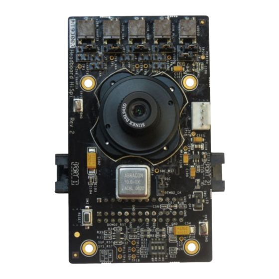
The evaluation boards are designed to demonstrate the features of
ON Semiconductor's image sensors products. This headboard is
intended to plug directly into the Demo 2X system. Test points and
jumpers on the board provide access to the clock, I/Os, and other
miscellaneous signals.
Features
•
Clock Input
Default – 10 MHz Crystal Oscillator
♦
Optional Demo 2X Controlled MClk
♦
•
Two Wire Serial Interface
Selectable Base Address
♦
•
Parallel Interface
•
HiSPi (High Speed Serial Pixel) Interface
•
ROHS Compliant
Block Diagram
HiSPi
(HiSPi)
RJ45
© Semiconductor Components Industries, LLC, 2016
July, 2016 − Rev. 0
SOC_RST_L
IMAGE
SOC_EXTCLK
2
I
C
EPROM
Figure 2. Block Diagram of MT9J003I12STMVH−GEVB
EVAL BOARD USER'S MANUAL
Figure 1. MT9J003 Evaluation Board
+3V3_HiSPi
+3V3_SERIAL
+2V8_PLL
+2V8_VAAPIX
+2V8_PLL
+1V8_SOC
+VDDIO_SOC
+VDDIO_PERIPH
+0V4
SYS_RST_L
IMAGE
SOC_EXTCLK
Jumper
1
www.onsemi.com
+5VD_BUS
Power
Supply
Reset
Supervisor
DEMO2_RST_L
DEMO2_MCLK
OSC_CLK
OSC
Socket
2
I
C
Publication Order Number:
EVBUM2421/D
Advertisement

Related Manuals for ON Semiconductor MT9J003


Summary of Contents for ON Semiconductor MT9J003
- Page 1 Evaluation Board Overview www.onsemi.com The evaluation boards are designed to demonstrate the features of ON Semiconductor’s image sensors products. This headboard is EVAL BOARD USER’S MANUAL intended to plug directly into the Demo 2X system. Test points and jumpers on the board provide access to the clock, I/Os, and other miscellaneous signals.
- Page 2 MT9J003I12STMVH−GEVB Top View +2V8_PLL JP6 +1V8_SOC JP3 +2V8_VAA JP2 +VDDIO_SOC JP5 +2V8_VAAPIX JP4 TEST J8 ATEST J7 GPIOs J6 SHUTTER J5 +VPP J4 CLK_SELECT JP1 ON_LED SW3 RESET SW2 EEPROM ADDR SW1 Figure 3. Top View of Evaluation Board − Default Jumpers Bottom View HiSPi Connector J50 HiSPi Connector J51...
- Page 3 MT9J003I12STMVH−GEVB Jumper Pin Locations The jumpers on headboards start with Pin 1 on the leftmost side of the pin. Grouped jumpers increase in pin size with each jumper added. Pin 1 Pins 1−4 Figure 5. Pin Locations for a Single Jumper. Pin 1 is Located at the Leftmost Side and Increases as it Moves to the Right Pin 1 Pins 1 and 2...
- Page 4 P24 Closed, EEPROM Address set to 0xA0 P23 Closed, P27 Closed RESET When pushed, 200 ms reset signal will be sent to MT9J003 ON_LED On (Default) Turns on +5V LED indicator Turns off +5V LED indicator Interfacing to ON Semiconductor Demo 2X Baseboard with P1 and P2 of the headboard.
-
Page 5: Technical Support
LIMITATIONS OF LIABILITY: ON Semiconductor shall not be liable for any special, consequential, incidental, indirect or punitive damages, including, but not limited to the costs of requalification, delay, loss of profits or goodwill, arising out of or in connection with the board, even if ON Semiconductor is advised of the possibility of such damages. In no event shall ON Semiconductor’s aggregate liability from any obligation arising out of or in connection with the board, under any theory of liability, exceed the purchase price paid for the board, if any.
Need help?
Do you have a question about the MT9J003 and is the answer not in the manual?
Questions and answers