Table of Contents
Advertisement
Quick Links
Advertisement
Table of Contents

Related Manuals for Texas Instruments THS4500EVM


Summary of Contents for Texas Instruments THS4500EVM
- Page 1 THS4500EVM User’s Guide June 2002 SLOU127...
- Page 2 IMPORTANT NOTICE Texas Instruments Incorporated and its subsidiaries (TI) reserve the right to make corrections, modifications, enhancements, improvements, and other changes to its products and services at any time and to discontinue any product or service without notice. Customers should obtain the latest relevant information before placing orders and should verify that such information is current and complete.
- Page 3 EVM IMPORTANT NOTICE Texas Instruments (TI) provides the enclosed product(s) under the following conditions: This evaluation kit being sold by TI is intended for use for ENGINEERING DEVELOPMENT OR EVALUATION PURPOSES ONLY and is not considered by TI to be fit for commercial use. As such, the goods being provided may not be complete in terms of required design-, marketing-, and/or manufacturing-related protective considerations, including product safety measures typically found in the end product incorporating the goods.
- Page 4 EVM schematic located in the EVM User’s Guide. When placing measurement probes near these devices during operation, please be aware that these devices may be very warm to the touch. Mailing Address: Texas Instruments Post Office Box 655303 Dallas, Texas 75265 Copyright 2002, Texas Instruments Incorporated...
- Page 5 It is recommended that the user initially review the data sheet of the device under test. It is helpful to review the schematic and layout of the THS4500EVM to determine the design techniques used in the evaluation board. It is recommended that the user review the application note Fully Differential Amplifiers (literature number SLOA054) to gain more insight about differential amplifiers.
- Page 6 Related Documentation From Texas Instruments This is an example of a warning statement. A warning statement describes a situation that could potentially cause harm to you. The information in a caution or a warning is provided for your protection. Please read each caution and warning carefully.
- Page 7 Trademarks Application report (literature number SLMA002), Power Pad Thermally Enhanced Package, http://www−s.ti.com/sc/psheets/slma004/slma002.pdf Application report (literature number SLMA004), PowerPAD Made Easy, http://www−s.ti.com/sc/psheets/slma004/slma004.pdf Application report (literature number SSYA008), Electrostatic Discharge (ESD), http://www−s.ti.com/sc/psheets/ssya008/ssya008.pdf Trademarks PowerPAD is a trademark of Texas Instruments.
-
Page 9: Table Of Contents
..........THS4500EVM Operating Conditions . - Page 10 5−1. Top Layer 1 (Signals for THS4500EVM) ......... .
-
Page 11: Introduction And Description
Introduction and Description 1 - 1 Introduction and Description... -
Page 12: Description
Description 1.1 Description The THS4500 EVM provides a platform for developing high-speed FDA application circuits. It contains the THS4500 high-speed FDA, a number of passive components, and various features and footprints that enable the user to experiment, test, and verify various operational amplifier circuit implementations. -
Page 13: Evm Default Configuration
EVM Default Configuration 1.4 EVM Default Configuration As delivered, the EVM has a fully functional example circuit, just add power supplies, a signal source, and monitoring instrument. See Figure 1−1 for the default schematic diagram. The user can change the gain by changing the ratios of the feedback and gain resistors (see the device data sheet for recommended resistor values). - Page 15 Chapter 2 Using the THS4500EVM This section describes how to connect the THS4500EVM to test equipment. It is recommended that the user connect the EVM as described in this section to avoid damage to the EVM or the THS4500 installed on the board.
-
Page 16: Required Equipment
Required Equipment 2.1 Required Equipment One dual-output dc power supply (±5 V, 1 A output minimum) One single-output dc power supply (5 V, 1 A output minimum). This power supply is used to activate the power-down function of the EVM, and will be referred to in the text of this document as the power-down supply. -
Page 17: Power Supply Connection For ±5 Vdc
Power Supply Connection Figure 2−1. Power Supply Connection for ±5 Vdc Using the THS4500EVM... -
Page 18: Function Generator Setup
Function Generator Setup 2.3 Function Generator Setup Note: The oscilloscope channels (CH1 and CH2) must be set to 50-Ω input imped- ance for proper results. 1) Connect the function generator to oscilloscope channel 1. 2) Set vertical channels 1 and 2 of the oscilloscope to 0.2 V/division and the time base to 0.1 µs/division. -
Page 19: Ths4500Evm Applications
Chapter 3 THS4500EVM Applications Example applications will be presented in this chapter. These applications are meant to demonstrate the most popular circuits to the user, but many other cir- cuits can be constructed. The user is encouraged to experiment with different circuits, exploring new and creative design techniques. -
Page 20: Single-Ended In/Single-Ended Out, Utilizing Transformer
3.1 Single-Ended In/Single-Ended Out, Utilizing Transformer The fully differential amp output can be monitored by a single-ended instrument at J4. The THS4500EVM utilizes Mini-Circuits CD542 footprint transformers to make the fully differential-to-single-ended conversion. An ADP4−1WT transformer is installed on the board. -
Page 21: Single Supply Operation
Single-Ended to Fully Differential Application Figure 3−2. Single Supply Operation Vocm 392 W 1 m F R6 0 C1 0 Vin− 374 W Vout+ − 56.2 W Vocm C2 0 THS4500 402 W Vout− 392 W THS4500EVM Applications... -
Page 23: High-Speed Amplifier Pcb Layout Tips
Chapter 4 High Speed Amplifier PCB Layout Tips The THS4500EVM layout has been designed for use with high-speed signals and can be used as an example when designing PCBs incorporating the THS4500. Careful attention has been given to component selection, grounding, power supply bypassing, and signal path layout. - Page 24 Circuit pathways should be made as symmetrical as possible for both feedback pathways to minimize second and other even harmonic content. The printed-circuit board that is be used with PowerPAD packages must have features included in the design to remove the heat from the package efficiently. As a minimum, there must be an area of solder-tinned-copper underneath the PowerPAD package.
-
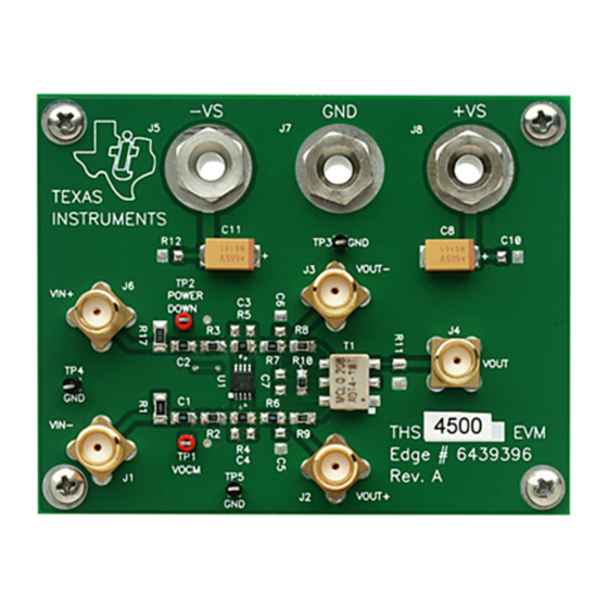
Page 25: Evm Hardware Description
Chapter 5 EVM Hardware Description This chapter describes the EVM hardware. It includes the EVM parts list, and printed circuit board layout. Table 5−1. THS4500EVM Bill of Materials Reference Manufacturer’s Distributor’s Size Designator Qty. Part Number Part Number Item Description CAP, 6.8 µF, tanatalum,... - Page 26 J1, J2, J3, J4, (Amphenol) (Newark) Jack 901−144−8RFX 01F2208 Standoff, 4−40 Hex, (Keystone) (Allied) 0.625” Length 1804 839−2089 Screw, Phillips, 4−40, SHR−0440−016−SN 0.250” IC, THS4500 (TI) THS4500DGN Board, printed circuit (TI) EDGE # 6439396 Figure 5−1. Top Layer 1 (Signals for THS4500EVM)
- Page 27 Figure 5−2. Bottom Layer 2 (Ground and Signal) EVM Hardware Description...
-
Page 28: Schematic Diagram
Figure 5−3. Schematic Diagram VCC+ VCC+ Vocm PD− 1 m F 392 W Vout+ R6 0 C1 0 Vin− 374 W 340 W Vout − 56.2 W Vocm 280 W C2 0 Vin+ 340 W 402 W ADP4 −1WT THS4500 −VS Vout−...
Need help?
Do you have a question about the THS4500EVM and is the answer not in the manual?
Questions and answers