Table of Contents
Advertisement
Quick Links
Advertisement
Table of Contents

Related Manuals for Epson RA8900SA/CE


Summary of Contents for Epson RA8900SA/CE
- Page 1 ETM44E-01 Application Manua Real Time Clock Module RA8900SA/CE Preliminary...
- Page 2 The information about applied circuitry, software, usage, etc. written in this material is intended for reference only. Seiko Epson does not assume any liability for the occurrence of infringing on any patent or copyright of a third party. This material does not authorize the licensing for any patent or intellectual copyrights.
-
Page 3: Table Of Contents
RA8900 SA / CE Contents 1. Overview ....................................1 2. Block Diagram ..................................1 3. Terminal description ................................2 3.1. Terminal connections ............................. 2 3.2. Pin Functions ................................2 4. Absolute Maximum Ratings ..............................3 5. Recommended Operating Conditions ............................ 3 6. -
Page 4: Overview
RA8900 SA / CE For automotive I C-Bus Interface Real-time Clock Module RA8900 SA / CE Features built-in 32.768 kHz DTCXO, High Stability. Supports I C-Bus's high speed mode (400 kHz) Alarm interrupt function for day, date, hour, and minute settings ... -
Page 5: Terminal Description
RA8900 SA / CE 3. Terminal description 3.1. Terminal connections RA890 0SA RA8900CE 1. T1 (CE) 14. N.C. 1. FOE 10. / INT 2. SCL 13. SDA 2. V 9. GND 3. FOUT 12. T2 (V 3. V 8. T2 (V 4. -
Page 6: Absolute Maximum Ratings
RA8900 SA / CE 4. Absolute Maximum Ratings GND=0V Item Symbol Condition Rating Unit 0.3 to +6.5 Supply voltage (1) Between V and GND 0.3 to +6.5 Supply voltage (2) Between V and GND Input voltage (2) FOE,SCL, SDA pins GND0.3 to +6.5 Output voltage (1) FOUT pin... -
Page 7: Electrical Characteristics
RA8900 SA / CE 7. Electrical Characteristics 7.1. DC Characteristics =2.5Vto5.5V,Ta=40Cto+85C *Unless otherwise specified, GND=0V,V Item Symbol Condition Min. Typ. Max. Unit Current = 0 Hz, / INT = V 0.72 1.50 =5 V DD consumption (1) FOE = GND, V A Current FOUT : output OFF (High Z) -
Page 8: Ac Characteristics
RA8900 SA / CE * Unless otherwise specified, 7.2. AC Characteristics =V GND=0V,V =1.6Vto5.5V,Ta=40Cto+85C Item Symbol Condition Min. Typ. Max. Unit SCL clock frequency s Start condition setup time SU;STA s Start condition hold time HD;STA Data setup time SU;DAT Data hold time HD;DAT s... -
Page 9: Use Methods
RA8900 SA / CE 8. Use Methods 8.1. Description of Registers 8.1.1. Write / Read and Bank Select … C Address 00h to 0Fh : Basic time and calendar register ompatible with RX-8803. Address 10h to 1Fh : Extension register 8.1.2. -
Page 10: Register Table (Extension Register)
RA8900 SA / CE 8.1.3. Register table (Extension register) Read Write Address Function bit 7 bit 6 bit 5 bit 4 bit 3 bit 2 bit 1 bit 0 HOUR WEEK MONTH ... -
Page 11: Details Of Registers
RA8900 SA / CE 8.2. Details of Registers 8.2.1. Clock counter (SEC - HOUR ) Address Function bit 7 bit 6 bit 5 bit 4 bit 3 bit 2 bit 1 bit 0 00, 10 01, 11 02, 12 HOUR ... -
Page 12: Calendar Counter ( Week - Year )
RA8900 SA / CE 8.2.2. Calendar counter ( WEEK - YEAR ) Address Function bit 7 bit 6 bit 5 bit 4 bit 3 bit 2 bit 1 bit 0 03, 13 WEEK ) "o" indicates write-protected bits. A zero is always read from these bits. 1) Day of the WEEK counter ... -
Page 13: Alarm Registers
RA8900 SA / CE 8.2.3. Alarm registers Address Function bit 7 bit 6 bit 5 bit 4 bit 3 bit 2 bit 1 bit 0 08, 18 MIN Alarm 09, 19 HOUR Alarm WEEK Alarm 0A, 1A DAY Alarm ... -
Page 14: Flag Register
RA8900 SA / CE 5) FSEL0,1 ( FOUT frequency Select 0, 1 ) bits The combination of these two bits is used to set the FOUT frequency. FSEL1 FSEL0 FSEL0,1 FOUT frequency (bit 3) (bit 2) 32768HzOutput Default 1024HzOutput Write/Read 1HzOutput 32768HzOutput 6) TSEL0,1 ( Timer Select 0, 1 ) bits... -
Page 15: Control Register
RA8900 SA / CE Data Description The VLF bit is cleared to zero to prepare for the next status detection. Write This bit is invalid after a "1" has been written to it. Data loss is not detected. Read Data loss is detected. All registers must be initialized. ( This setting is retained until a "zero"... - Page 16 RA8900 SA / CE Data Function When a time update interrupt event occurs, an interrupt signal is not generated or is canceled (/INT status changes from low to Hi-Z). When a time update interrupt event occurs, an interrupt signal is generated Write/Read (/INT status changes from Hi-Z to low).
-
Page 17: Temperature Data Register
RA8900 SA / CE 8.2.8. Temperature Data register Address Function bit 7 bit 6 bit 5 bit 4 bit 3 bit 2 bit 1 bit 0 TEMP 1) Temperature Data register This register can begin to read digital temperature data. The temperature data are updated in an operation timing of the temperature compensation circuit. -
Page 18: Fixed-Cycle Timer Interrupt Function
RA8900 SA / CE 8.3. Fixed-cycle Timer Interrupt Function The fixed-cycle timer interrupt generation function generates an interrupt event periodically at any fixed cycle set between 244.14s and 4095 minutes. When an interrupt event is generated, the /INT pin goes to low level and "1" is set to the TF bit to report that an event has occurred. -
Page 19: Related Registers For Function Of Time Update Interrupts
RA8900 SA / CE 8.3.2. Related registers for function of time update interrupts. Address Function bit 7 bit 6 bit 5 bit 4 bit 3 bit 2 bit 1 bit 0 0B, 1B Timer Counter 0 0C, 1C Timer Counter 1 2048... -
Page 20: Fixed-Cycle Timer Interrupt Interval (Example)
RA8900 SA / CE 5) TIE (Timer Interrupt Enable) bit When a fixed-cycle timer interrupt event occurs (when the TF bit value changes from "0" to "1"), this bit's value specifies whether an interrupt signal is generated (/INT status changes from Hi-Z to low) or is not generated (/INT status remains Hi-Z). -
Page 21: Time Update Interrupt Function
RA8900 SA / CE 8.4. Time Update Interrupt Function The time update interrupt function generates interrupt events at one-second or one-minute intervals, according to the timing of the internal clock. When an interrupt event occurs, the UF bit value becomes "1" and the /INT pin goes to low level to indicate that an event has occurred. -
Page 22: Related Registers For Time Update Interrupt Functions
RA8900 SA / CE 8.4.2. Related registers for time update interrupt functions. Address Function bit 7 bit 6 bit 5 bit 4 bit 3 bit 2 bit 1 bit 0 0D, 1D Extension Register USEL TEST WADA FSEL1 FSEL0 TSEL1 TSEL0 0E, 1E Flag Register... -
Page 23: Alarm Interrupt Function
RA8900 SA / CE 8.5. Alarm Interrupt Function The alarm interrupt generation function generates interrupt events for alarm settings such as date, day, hour, and minute settings. When an interrupt event occurs, the AF bit value is set to "1" and the /INT pin goes to low level to indicate that an event has occurred. -
Page 24: Related Registers
RA8900 SA / CE 8.5.2. Related registers Address Function bit 7 bit 6 bit 5 bit 4 bit 3 bit 2 bit 1 bit 0 01, 12 02, 13 HOUR 03, 14 WEEK 04, 15 ... -
Page 25: Examples Of Alarm Settings
RA8900 SA / CE 3) AF (Alarm Flag) bit When this flag bit value is already set to "0", occurrence of an alarm interrupt event changes it to "1". When this flag bit value is "1", its value is retained until a "0" is written to it. Data Description The AF bit is cleared to zero to prepare for the next status detection... -
Page 26: About The Interrupt Function For Operation /Int="L" Interrupt Output
RA8900 SA / CE 8.6. About the interrupt function for operation /INT=”L” interrupt output. How to identify events when the interrupt output occurred. /INT output pin is common output terminal of interrupt events of three types (Fixed-cycle timer Time interrupt , alarm interrupt, time update interrupt). -
Page 27: Battery Backup Switchover Function
RA8900 SA / CE 8.8. Battery backup switchover function 8.8.1. Description of Battery backup switchover function It consists of the power-source detector "VDET" which detect the power down of the main power source "VDD", and built-in MOS switches located between the main power-source pin "VDD" and the backup power supply pin "VBAT". In turning off a MOS switch according to the supply-voltage detection result of VDET, when an drive power source changes to VDD OFF ->VBAT (it shifts to a backup operation from a normal operation), it becomes possible to prevent a reverse-current (VBAT->VDD) of an electric current. -
Page 28: Control The Contents Of The Power Switching
RA8900 SA / CE 8.8.2. Control the contents of the power switching BACKUP state PMOS switch is turned off at all times. Voltage detection VDET3 is responsible for monitoring every 1sec. This state will be selected at cold start. Make the voltage detection for the first time in 1sec after since it was powered on VDD pin. -
Page 29: Notes On Power Switching Function Is Used
RA8900 SA / CE 8.8.4. Notes on power switching function is used 1.Please make VDD = 0V, when you backup. If the VDD voltage is lower than VACCSW(2), there is an unnecessary current flows through the input and output circuit. The transition to the backup from NORMAL state, please set to VDD = 0V promptly. Also, when returning from a backup, please set to VDD level of desired promptly. -
Page 30: Reading/Writing Data Via The I 2 C Bus Interface
RA8900 SA / CE 8.9. Reading/Writing Data via the I C Bus Interface 8.9.1. Overview of I C-BUS The I C bus supports bi-directional communications via two signal lines: the SDA (data) line and SCL (clock) line. A combination of these two signals is used to transmit and receive communication start/stop signals, data transfer signals, acknowledge signals, and so on. -
Page 31: Starting And Stopping I C Bus Communications
RA8900 SA / CE 8.9.3. Starting and stopping I C bus communications START Repeated START(RESTART) STOP condition condition condition [ S ] [ Sr ] [ P ] 0.95s ( Max. ) 1) START condition, repeated START condition, and STOP condition (1) START condition ... -
Page 32: Data Transfers And Acknowledge Responses During I 2 C-Bus Communications
RA8900 SA / CE 8.9.4. Data transfers and acknowledge responses during I C-BUS communications 1) Data transfers Data transfers are performed in 8-bit (1 byte) units once the START condition has occurred. There is no limit on the amount (bytes) of data that are transferred between the START condition and STOP condition. ( However, the transfer time must be no longer than 0.95 seconds .) The address auto increment function operates during both write and read operations. -
Page 33: I 2 C Bus Protocol
RA8900 SA / CE 8.9.6. I C bus protocol In the following sequence descriptions, it is assumed that the CPU is the master and the RA8900 is the slave. a. Address specification write sequence Since the RA8900 includes an address auto increment function, once the initial address has been specified, the RA8900 increments (by one byte) the receive address each time data is transferred. -
Page 34: Backup And Recovery
RA8900 SA / CE 8.10. Backup and Recovery * tR1 is restrictions to validate power-on reset. When cannot keep this standard, power-on reset does not work normally. It is necessary to initial setting by the software command. Repeated ON/OFF of the power supply in short term, the power-on reset becomes unstable. After power-OFF, keep a state of VDD=GND more than 60 seconds to validate power-on reset. -
Page 35: About Access At The Time Of Backup Return And Initial Power Supply
RA8900 SA / CE 8.11. About access at the time of backup return and Initial power supply Because of most of RTC registers synchronize to an oscillation clock of a built-in crystal oscillator , RTC does not work normally in a without inside oscillation. Please perform initial setting at the time of power supply voltage return from the state that an oscillation stopped after progress in oscillation start time. -
Page 36: Flow Chart
RA8900 SA / CE 8.12. Flow chart The following flow-chart is one instance. Mention for easy understanding takes precedence over others; therefore there are some inefficient cases for the actual processing. If you wish to take more efficient process, perform some processes at the same time or try to confirm and adjust some part where is no hindered from transposing of operation procedure. - Page 37 RA8900 SA / CE 2) Method of initialization after starting of internal oscillation The Initialize is possible in 30ms since Internal VDD becomes higher than bottom value of clock supply voltage. Even in this case, after an internal oscillation begins, it is necessary to clear VLF= “0”. power on ...
- Page 38 RA8900 SA / CE 3) The setting of a clock and calendar Set time Set RESET bit to “1” to prevent timer update in time setting. RESET"1" Write information of[year/month/date[day of the week]hour: minute: second] which is necessary to set (or reset). Write time In case of initialization, please initialize all data.
-
Page 39: Connection With Typical Microcontroller
RA8900 SA / CE 8.13. Connection with Typical Microcontroller Note I C-BUS Master RA8900 SLAVE ADRS = 0110 010* Pull up Registor C Bus ) Note : It uses the secondary battery or a lithium battery. For detailed value on the resistance, please consult a battery maker. 8.14. -
Page 40: External Dimensions/Marking Layout
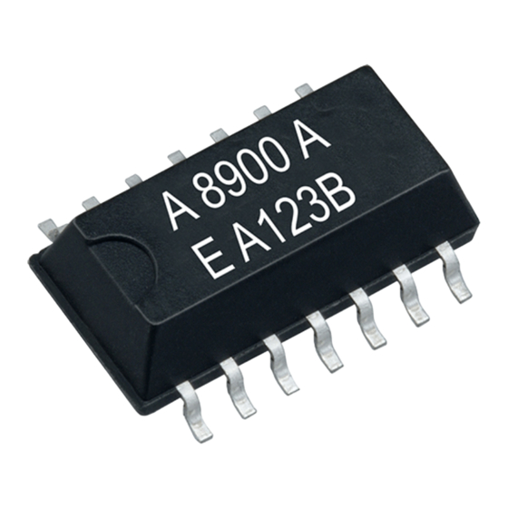
RA8900 SA / CE 9. External Dimensions/Marking Layout 9.1. RA8900SA 9.1.1. External dimensions RA8900SA ( SOP 14pin ) External dimensions Recommended soldering pattern 10.1 0 - 10 5.0 7.4 0.15 1.27 0.05 1.27 ... - Page 41 RA8900 SA / CE 9.2. RA8900CE 9.2.1. External dimensions RA8900CE External dimensions Recommended soldering pattern 0.35 Unit : mm 9.2.2. Marking layout RA8900CE UA : A Type L ogo Frequency UB : Blank Stability UC : C A8900 A...
-
Page 42: Application Notes
RA8900 SA / CE 10. Application notes 1) Notes on handling This module uses a C-MOS IC to realize low power consumption. Carefully note the following cautions when handling. (1) Static electricity While this module has built-in circuitry designed to protect it against electrostatic discharge, the chip could still be damaged by a large discharge of static electricity. - Page 43 Unit 715-723 7/F Trade Square, 681 Cheung Sha Wan Road, Kowloon, Hong Kong Phone: (86) 755-2699-3828 (Shenzhen Branch) Fax: (86) 755-2699-3838 (Shenzhen Branch) http://www.epson.com.hk EPSON TAIWAN TECHNOLOGY & TRADING LTD. 14F, No.7, Song Ren Road, Taipei 110 Phone: (886) 2-8786-6688 Fax: (886)2-8786-6660 http://www.epson.com.tw/ElectronicComponent EPSON SINGAPORE PTE.
- Page 44 Partner in Electronic Components & Supply Chain Solutions The Netherlands Denmark Elektrostraat 17 Sdr. Jagtvej 12 NL-7483 PG Haaksbergen DK-2970 Hørsholm Tel: +31 (0)53 573 33 33 Tel: +45 88 20 26 30 Fax: +31 (0)53 573 33 30 Fax: +45 88 20 26 39 nl@texim-europe.com nordic@texim-europe.com...
Need help?
Do you have a question about the RA8900SA/CE and is the answer not in the manual?
Questions and answers