Table of Contents
Advertisement
Quick Links
CD RECEIVER
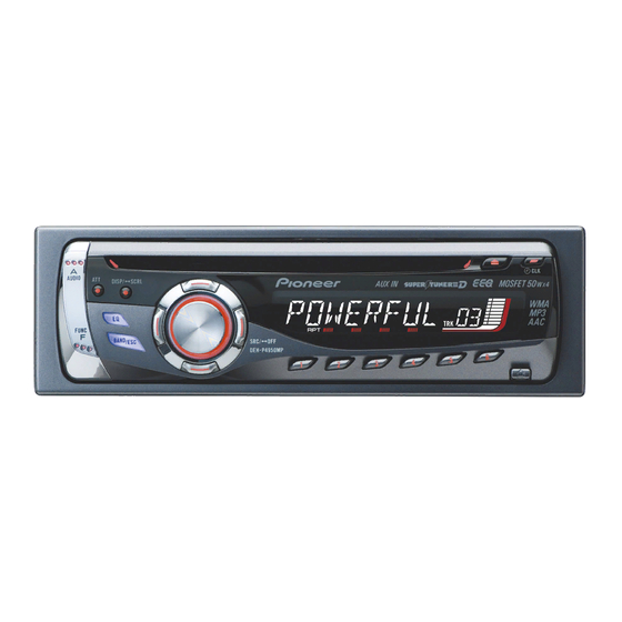
DEH-P4950MP
This service manual should be used together with the following manual(s):
Model No.
Order No.
CX-3195
CRT3815
For details, refer to "Important Check Points for Good Servicing".
PIONEER CORPORATION
PIONEER ELECTRONICS (USA) INC. P.O. Box 1760, Long Beach, CA 90801-1760, U.S.A.
PIONEER EUROPE NV Haven 1087, Keetberglaan 1, 9120 Melsele, Belgium
PIONEER ELECTRONICS ASIACENTRE PTE. LTD. 253 Alexandra Road, #04-01, Singapore 159936
PIONEER CORPORATION 2006
Mech.Module
S10.5COMP2
CD Mech. Module : Circuit Descriptions, Mech. Descriptions, Disassembly
4-1, Meguro 1-chome, Meguro-ku, Tokyo 153-8654, Japan
DEH-P4950MP/XU/ES
Remarks
ORDER NO.
CRT3835
/XU/ES
K-ZZA. NOV. 2006 Printed in Japan
Advertisement
Table of Contents

Subscribe to Our Youtube Channel
Related Manuals for Pioneer DEH-P4950MP/XU


Summary of Contents for Pioneer DEH-P4950MP/XU
- Page 1 PIONEER CORPORATION 4-1, Meguro 1-chome, Meguro-ku, Tokyo 153-8654, Japan PIONEER ELECTRONICS (USA) INC. P.O. Box 1760, Long Beach, CA 90801-1760, U.S.A. PIONEER EUROPE NV Haven 1087, Keetberglaan 1, 9120 Melsele, Belgium PIONEER ELECTRONICS ASIACENTRE PTE. LTD. 253 Alexandra Road, #04-01, Singapore 159936 PIONEER CORPORATION 2006 K-ZZA.
-
Page 2: Safety Information
(shorting-solder) by referring to "the DISASSEMBLY". 4. After replacing the pickup unit, be sure to check the grating. 5. Be careful in handling ICs. Some ICs such as MOS type are so fragile that they can be damaged by electrostatic induction. DEH-P4950MP/XU/ES... - Page 3 To protect products from damages or failures during transit, the shipping mode should be set or the shipping screws should be installed before shipment. Please be sure to follow this method especially if it is specified in this manual. DEH-P4950MP/XU/ES...
-
Page 4: Table Of Contents
7. GENERAL INFORMATION ..........................49 7.1 DIAGNOSIS ............................. 49 7.1.1 DISASSEMBLY ............................. 49 7.1.2 CONNECTOR FUNCTION DESCRIPTION ..................52 7.2 PARTS..............................53 7.2.1 IC ................................53 7.2.2 DISPLAY ............................... 62 7.3 OPERATIONAL FLOW CHART ....................... 63 8. OPERATIONS ..............................64 DEH-P4950MP/XU/ES... -
Page 5: Specifications
1. SPECIFICATIONS DEH-P4950MP/XU/ES... -
Page 6: Exploded Views And Parts List
• Screw adjacent to mark on the product are used for disassembly. • For the applying amount of lubricants or glue, follow the instructions in this manual. (In the case of no amount instructions,apply as you think it appropriate.) 2.1 PACKING DEHP4950MPXUESpacking 15 14 DEH-P4950MP/XU/ES... - Page 7 20-2 Owner's Manual YRD5114 Polyethylene Bag CEG-127 20-3 Owner's Manual YRD5115 20-4 Installation Manual YRD5116 Screw CRZ50P090FTC Screw TRZ50P080FTC Owner's Manual,Installation Manual Part No. Language YRD5114 English, Spanish, Portuguese(B) YRD5115 Traditional Chinese, Arabic YRD5116 English, Spanish, Portuguese(B), Traditional Chinese, Arabic DEH-P4950MP/XU/ES...
-
Page 8: Exterior
2.2 EXTERIOR DEH-P4950MP/XU/ES DEH-P4950MP/XU/ES... - Page 9 Panel Unit YXA5154 Button(DETACH) CAC4836 Spring CBH1835 Spring CBH2208 Spring CBH2367 Bracket CNC6791 Holder CNC8042 Cover CNM6276 CNV4692 CNV4728 CNV5576 Screw IMS20P030FTB Detachable Assy YXA5221 Screw BPZ20P080FTB Spring CBH2210 Knob(SOURCE, VOLUME) YAA5008 Button(1-6) YAC5187 Button(EQ, BAND/ESC) YAC5075 Button(ATT, DISP/SCRL) YAC5076 DEH-P4950MP/XU/ES...
-
Page 10: Cd Mechanism Module
2.3 CD MECHANISM MODULE DEH-P4950MP/XU/ES... - Page 11 Bracket CND2583 CND2584 Lever CND2585 CND2586 Bracket CND2587 CND2588 Lever CND2589 Holder CNV7201 Gear CNV7207 Gear CNV7208 Gear CNV7209 Gear CNV7210 Gear CNV7211 Gear CNV7212 Rack CNV7214 CNV7216 Roller CNV8189 Gear CNV7219 Guide CNV7361 Gear CNV7595 Guide CNV8448 CNV7805 DEH-P4950MP/XU/ES...
-
Page 12: Block Diagram And Schematic Diagram
SD,MD VDD5 NJM2885DL1-33 /PUEN SPINDLE MOTOR LOEJ /RESET RESET LOEJ /RESET CDRST CLCONT CLCONT LCOP CARRIAGE LOAD/ MOTOR LCOM CONT BRST,BRXEN,BSRQ BRST,BRXEN,BSRQ,BDATA,BSCK CONT BDATA,BSCK Q702 B.UP 12EJ Q701 DSCSNS HOME VCCONT S904 S905 S901 12EJ HOME S903 DSCSNS VDSENS DEH-P4950MP/XU/ES... - Page 13 ILMPW SWVDD S1827 SSENS REM.CON. B.UP SSENS IC1802 ROT1 ROT1 ROT1 TSOP4840SB1 ROT0 ROT0 ROT0 VCCONT VOLUME KEY DATA /SOURCE X1801 5MHz DPDT DPDT LCD DRIVER/ DPDT DPDT KEY CONTROLLER KYDT KYDT IC 1801 KYDT KYDT PD6340A VLCD LCD1801 DEH-P4950MP/XU/ES...
-
Page 14: Overall Connection Diagram(Guide Page)
Note: When ordering service parts, be sure to refer to " EXPLODED VIEWS AND PARTS LIST" or "ELECTRICAL PARTS LIST". Large size SCH diagram FM(10%) : -33.5 dB AM(15%) : -30.0 dB CN701 CD(-20 dB) : -19.4 dB Guide page Detailed page AUX IN(-20 dB) : -17.8 dB IP-BUS(-20 dB) : -17.8 dB CN1801 DEH-P4950MP/XU/ES... - Page 15 No differentiation is made between chip capacitors and discrete capacitors. For resistors and capacitors in the circuit diagrams, their resistance values or capacitance values are expressed in codes: Ex. *Resistors Code Practical value 12k ohms 10k ohms *Capacitors Code Practical value 0.01uF 101/10 100uF/10V DEH-P4950MP/XU/ES...
- Page 16 DEH-P4950MP/XU/ES...
- Page 17 DEH-P4950MP/XU/ES...
- Page 18 DEH-P4950MP/XU/ES...
- Page 19 DEH-P4950MP/XU/ES...
-
Page 20: Keyboard Unit
3.3 KEYBOARD UNIT LCD DRIVER/ KEY CONTROLLER DEH-P4950MP/XU/ES... - Page 21 KEYBOARD UNIT CN804 CLOCK DEH-P4950MP/XU/ES...
-
Page 22: Cd Mechanism Module(Guide Page)
3.4 CD MECHANISM MODULE(GUIDE PAGE) PICKUP UNIT(P10.5)(SERVICE) SWITCHES: CD CORE UNIT(S10.5COMP2) S901:HOME SWITCH..ON-OFF S903:DSCSNS SWITCH..ON-OFF S904:12EJ SWITCH.....ON-OFF S905:8EJ SWITCH....ON-OFF The underlined indicates the switch position. M1 CXC7134 SPINDLE MOTOR M2 CXC4026 LOADING/CARRIAGE MOTOR CD DRIVER DEH-P4950MP/XU/ES... - Page 23 CD CORE UNIT(S10.5COMP2) SIGNAL LINE FOCUS SERVO LINE TRACKING SERVO LINE CARRIAGE SERVO LINE SPINDLE SERVO LINE CN701 & DEH-P4950MP/XU/ES...
- Page 24 DEH-P4950MP/XU/ES...
- Page 25 DEH-P4950MP/XU/ES...
- Page 26 DEH-P4950MP/XU/ES...
- Page 27 DEH-P4950MP/XU/ES...
- Page 28 200 ms/div 500 mV/div 2 ms/div 1 V/div %RFAGC 500 mV/div 500 mV/div 500 mV/div 9TIN 500 mV/div Focus Search waveform Track Open waveform 1 Track Jump waveform Ref.: Ref.: Ref.: REFO REFO REFO Mode: Mode: Mode: TEST TEST TEST DEH-P4950MP/XU/ES...
- Page 29 4LOEJ 312SNS 5 V/div 5 V/div 1 V/div 4LOEJ 0FIN 5 V/div 1 V/div Black dot(800 μm) during play 12 cm CD Eject operation 8 cm CD Eject operation Ref.: Ref.: Ref.: REFO Mode: Mode: Mode: Normal Normal Normal DEH-P4950MP/XU/ES...
-
Page 30: Pcb Connection Diagram
For further information for respective destinations, be sure to check with the schematic dia- gram. CORD ASSY 2.Viewpoint of PCB diagrams Capacitor Connector IP-BUS INPUT SIDE A SIDE B Chip Part P.C.Board CN701 DSENS DEH-P4950MP/XU/ES... - Page 31 SIDE A REAR OUTPUT FRONT OUTPUT SUBWOOFER OUTPUT ANTENNA CN1902 FRONT DEH-P4950MP/XU/ES...
- Page 32 TUNER AMP UNIT >FU353 (B,131,131) Fuse 3 A CEK1286 TEST DEH-P4950MP/XU/ES...
- Page 33 SIDE B DEH-P4950MP/XU/ES...
-
Page 34: Keyboard Unit
4.2 KEYBOARD UNIT KEYBOARD UNIT SIDE A KEYBOARD UNIT SIDE B CN804 DEH-P4950MP/XU/ES... - Page 35 DEH-P4950MP/XU/ES...
-
Page 36: Cd Core Unit(S10.5Comp2)
4.3 CD CORE UNIT(S10.5COMP2) CD CORE UNIT(S10.5COMP2) SIDE A CN701 PICKUP UNIT(P10.5)(SERVICE) LOADING /CARRIAGE MOTOR SPINDLE MOTOR DEH-P4950MP/XU/ES... - Page 37 CD CORE UNIT(S10.5COMP2) SIDE B DEH-P4950MP/XU/ES...
-
Page 38: Electrical Parts List
(B,125,24) Transistor 2SA1036K R 102 (B,33,98) RS1/16S222J Q 842 (B,120,26) Transistor DTC114EUA R 103 (B,25,127) RS1/16S181J R 104 (B,36,132) RS1/16S101J Q 851 (B,36,11) Transistor 2SA1036K R 105 (B,33,133) RS1/16S101J Q 852 (B,36,7) Transistor DTC114EUA Q 911 (A,6,99) Transistor 2SD2396 DEH-P4950MP/XU/ES... - Page 39 R 602 (B,68,42) RS1/16S103J R 937 (B,62,116) RS1/16S473J R 604 (B,97,62) RS1/16S681J R 938 (B,60,121) RS1/4SA102J R 605 (B,153,59) RS1/16S681J R 961 (B,70,34) RS1/16S102J R 607 (B,145,56) RS1/16S681J R 962 (B,62,37) RS1/16S822J R 609 (B,98,43) RS1/16S104J R 610 (B,104,50) RS1/16S473J DEH-P4950MP/XU/ES...
- Page 40 (A,36,28) Push Switch CSG1155 S 1803 (A,43,80) Push Switch CSG1155 C 703 (A,30,27) CEJQ101M10 S 1804 (A,42,118) Push Switch CSG1155 C 704 (B,144,73) CKSRYB105K10 S 1805 (A,43,93) Push Switch CSG1155 C 705 (B,126,74) CKSRYB105K10 S 1806 (A,25,62) Push Switch CSG1155 DEH-P4950MP/XU/ES...
- Page 41 (B,24,68) Switch(8EJ) CSN1068 C 218 (A,49,51) CKSSYB473K10 C 219 (A,45,53) CKSSYB104K10 RESISTORS C 220 (A,46,53) CKSSYB182K50 C 221 (A,44,53) CKSSYB104K10 C 222 (B,43,53) CCSSCH560J50 R 101 (B,60,73) RS1/10SR2R4J R 102 (B,59,71) RS1/10SR2R4J C 223 (B,45,53) CCSSCH4R0C50 R 103 (B,60,71) RS1/10SR2R7J DEH-P4950MP/XU/ES...
- Page 42 C 303 (A,35,19) CKSSYB472K25 C 304 (A,34,21) CKSSYB223K16 C 307 (B,25,9) CKSRYB104K16 C 308 (B,10,27) CKSRYB105K10 C 703 (B,11,37) CCSSCH101J50 C 704 (B,8,36) CKSSYB102K50 C 711 (A,25,26) CKSSYB104K10 Miscellaneous Parts List Pickup Unit(P10.5)(Service) CXX1942 Motor Unit(SPINDLE) CXC7134 Motor Unit(LOADING/CARRIAGE) CXC4026 DEH-P4950MP/XU/ES...
-
Page 43: Adjustment
1k ohms in series. • The load and eject operation is not guarantied with the mechanism upside down. If the mechanism is blocked due to mistaken eject operation, reset the product or turn off and on the ACC to restore it. DEH-P4950MP/XU/ES... - Page 44 • When the power is turned on/off the jump mode is reset to the Single TR (91) while the gain of the RFAMP is reset to 0 dB. At the same time all the self-adjusting values shall return to the default setting. DEH-P4950MP/XU/ES...
-
Page 45: Checking The Grating After Changing The Pickup Unit
Because of eccentricity in the disc and a slight misalignment of the clamping center the grating waveform may be seen to "wobble" ( the phase difference changes as the disc rotates). The angle specified above indicates the average angle. • Hint Reloading the disc changes the clamp position and may decrease the "wobble". DEH-P4950MP/XU/ES... - Page 46 Ech → Xch 20 mV/div, AC Grating waveform Fch → Ych 20 mV/div, AC 0° 30° 45° 60° 75° 90° DEH-P4950MP/XU/ES...
-
Page 47: Error Mode
Remarks: Mechanical errors are not displayed (because a CD is turned off in these errors). Unreadable TOC does not constitute an error. An intended operation continues in this case. Upper digits of an error code are subdivided as shown below: 1x: Setup relevant errors, 3x: Search relevant errors, Ax: Other errors. DEH-P4950MP/XU/ES... -
Page 48: System Microcomputer Test Program
The frequency of the clock signal is 468 750 Hz that is one 32th of the fundamental frequency. The clock signal should be 468 750 Hz(- 10 Hz, + 15 Hz). If the clock signal is out of the range, the X'tal (X601) should be replaced with new one. DEH-P4950MP/XU/ES... -
Page 49: General Information
Release the two latchs and then remove the Grille Assy. Grille Assy Fig.1 Removing the Tuner Amp Unit (Fig.2) Remove the screw. Remove the three screws. Straighten the tabs at four locations indicated and then remove the Tuner Amp Unit. Tuner Amp Unit Fig.2 DEH-P4950MP/XU/ES... - Page 50 Upper Frame. 3. While lifting the Carriage Mechanism, remove it from the three Dampers. Caution: When assembling, be sure to apply some alcohol to the Dampers and assemble the mechanism in a clamped state. Damper Damper Carriage Mechanism Lower Frame DEH-P4950MP/XU/ES...
- Page 51 Assemble the sub unit side of the Pickup, taking the plate (Chassis) in-between. When treating the leads of the Load Carriage Motor Assy, do not make them loose over the Feed Screw. Poly Washer Change Arm Pickup Lock Arm Inner Holder Feed Screw Planet Gear Pickup Rack Chassis Pickup DEH-P4950MP/XU/ES...
-
Page 52: Connector Function Description
7.1.2 CONNECTOR FUNCTION DESCRIPTION DEH-P4950MP/XU/ES... -
Page 53: Parts
Stand-by P-GND2 Circuit OUT2- Offset Protector; STBY Detection Thermal OUT2+ OUT1- Offset P-GND1 Detection OUT1+ S-GND Protector; Short circuit AC-GND OUT3+ Offset P-GND3 Detection OUT3- OUT4+ Offset MUTE Detection OUT4- P-GND4 SWITCH Protector; Over current limit Mute circuit DEH-P4950MP/XU/ES... - Page 54 PML015B - Block Diagram - Pin Layout IN1_L IN1_R IN2_L IN2_R IN3_L IN3_R IN4+_L IN4+_R IN4-_R IN4-_L Front_R Front_L Rear_L Rear_R Vref DATA FIE_R FIE_L Pre/SW_R Pre/SW_L LMout PGND Pref DEH-P4950MP/XU/ES...
- Page 55 NJM2794V OUT1 IN1+ IN1- OUT1 IN1+ IN1- VREF Vref IN2- IN2+ OUT2 IN2- OUT2 IN2+ DEH-P4950MP/XU/ES...
- Page 56 E.VOL clock output E.VOL data output Not used ROM correction data input/output ROMDATA ROM correction clock output ROMCK ROMCS ROM correction chip select output Not used Power supply input(+) Not used TUNER : Chip enable output(EEPROM) TUNER : Chip enable output(PLL) DEH-P4950MP/XU/ES...
- Page 57 93,94 MODEL Model select input A/D converter GND(Connected to VSS) AVSS Signal level input(Field intensity) A/D converter reference voltage input VREF A/D converter power supply input terminal(Connected to VCC) AVCC Not used PEG298A Format Meaning CMOS Nch open drain DEH-P4950MP/XU/ES...
- Page 58 Crystal oscillator connection pin Crystal oscillator connection pin 25,26 KDT2,3 Key data input Not used KST4 Key strobe output 29-32 Not used 33-55 SEG35-13 LCD segment output Power supply 57-64 SEG12-5 LCD segment output PD6340A PE5547A Format Meaning CMOS Nch open drain DEH-P4950MP/XU/ES...
- Page 59 Power supply for the crystal oscillator Power supply for DAC DA.VDD Output of audio for the left channel LOUT Ground for DAC DA.GND Connected to the capacitor for band gap REGC DA.GND Ground for DAC Output of audio for the right channel ROUT DEH-P4950MP/XU/ES...
- Page 60 Output of reference voltage REFOUT Reversal input of FE Output of FE ADCIN FE,TE A/D converter input Reversal input of TE Output of TE Output of LD Input of PD AD.VDD Power supply for servo ADC Ground for servo ADC AD.GND DEH-P4950MP/XU/ES...
- Page 61 22 AUDIOGND audio ground Ground of audio block 23 L ch O L channel output FM stereo “L-ch” signal output or AM audio output 24 R ch O R channel output FM stereo “R-ch” signal output or AM audio output DEH-P4950MP/XU/ES...
-
Page 62: Display
7.2.2 DISPLAY - LCD(YAW5083) DEH-P4950MP/XU/ES... -
Page 63: Operational Flow Chart
In case of the above signal, the communication with Grille microcomputer may fail. Source keys If the time interval is not 300 msec, the oscillator operative may be defective. Source ON SYSPW←H Pin 48 Completes power-on operation. (After that, proceed to each source operation) DEH-P4950MP/XU/ES... -
Page 64: Operations
8. OPERATIONS DEH-P4950MP/XU/ES... - Page 65 (CXX1982) DEH-P4950MP/XU/ES...
- Page 66 - Connection Diagram DEH-P4950MP/XU/ES...
- Page 67 DEH-P4950MP/XU/ES...
- Page 68 CD Mechanism Module Before shipping out the product, be sure to clean the following portions by using the prescribed cleaning tools: Portions to be cleaned Cleaning tools CD pickup lenses Cleaning liquid : GEM1004 Cleaning paper : GED-008 g p p DEH-P4950MP/XU/ES...
Need help?
Do you have a question about the DEH-P4950MP/XU and is the answer not in the manual?
Questions and answers