
Subscribe to Our Youtube Channel
Related Manuals for Lucent Technologies 5ESS-2000


Summary of Contents for Lucent Technologies 5ESS-2000
- Page 1 2 5-105-510 July 1999 ® 5ESS -2000 Switch B21D Computer Hardware Reference Manual Document: 235-105-510 ssue Date: July 1999 ssue Number: 3.00A Copyright © 1999 Lucent Technologies Page 1...
- Page 2 Every effort was made to ensure that the information in this P was complete and accurate at the time of publication. However, information is subject to change. This P describes certain hardware, software, features, and capabilities of Lucent Technologies products. This P is for information purposes; therefore, caution is advised that this P may differ from any configuration currently installed.
- Page 3 Support Telephone Numbers nformation Product Support Telephone Number: To report errors or ask nontechnical questions about this or other Ps produced by Lucent Technologies, call 1-888-LT NFO6 (1-888-584-6366). Technical Support Telephone Numbers: For initial technical assistance, call the North American Regional Technical Assistance Center (NARTAC) at 1-800-225-RTAC (1-800-225-7822).
- Page 4 E13 software release. And Chapter 4 was reorganized into three chapters. (See Section 1. DOCUMENT ORGANIZATION.) The Lucent Technologies Network Systems organization reserves the right to revise this document for any reason. The reasons for revision will include, but are not limited to: conformity with standards declared by ANS , the...
- Page 5 See Support Telephone Numbers on the back of the front cover page of this document. 1.5 DISTRIBUTION This manual is distributed by the Lucent Technologies Customer nformation Center in ndianapolis, ndiana. Most operating telephone companies should place orders through their documentation coordinator. Some companies may allow customers to order directly from the Customer nformation Center;...
- Page 6 The 3B21D computer is a high-speed, high-reliability, fault-tolerant, duplex computer. t is a bit-compatible version of the 3B20D computer, which is used in various roles in Lucent Technologies switching products. All major functional units are duplicated to ensure uninterrupted and reliable service.
- Page 7 2 5-105-510 July 1999 Figure 2-1 B21D Computer System Block Diagram 2. .1 Control Unit (CU) Copyright © 1999 Lucent Technologies Page 2...
- Page 8 The Expansion (EX) slots provide an interface for new (future) hardware features to access the MAS and CC via the Central Control nput/Output (CC O) bus and the Main Store Bus (MASB). Each CU has two EX slots, EX 0 and EX 2. .1. Utility Circuit (UC) Copyright © 1999 Lucent Technologies Page...
- Page 9 Each channel supports four DSCH interfaces. 2. .2 Peripheral Devices Figure 2-1 shows three types of peripheral devices: nput/Output Processor ( OP) Disk File Controller (DFC) Communications Module/Communications Network nterface (CM/CN ). Copyright © 1999 Lucent Technologies Page 4...
- Page 10 One port switch is equipped in Processor Unit 1. n the 3B21D computer, the PSSBD is located in CU 1. (Note that in the 3B20D computer, the PSSBD is located in CU 0.) Copyright © 1999 Lucent Technologies Page 5...
- Page 11 The functional blocks shown in Figure 2-1 are physically represented by the following circuit pack designs: 410AA DC-to-DC converter circuit pack provides +5 V DC from -48 V DC. KBN10 nput/Output Processor ( OP) circuit pack contains the DSCH and OM interface functions. Copyright © 1999 Lucent Technologies Page 6...
- Page 12 Asynchronous Data Link Peripheral Controller that replaces the TN82B, TN74B, TN75C, and TN1839 circuit packs. UN58 Maintenance TTY Controller circuit pack that replaces the TN983. UN597 Maintenance TTY Controller circuit pack that replaces the UN583. Copyright © 1999 Lucent Technologies Page 7...
- Page 13 All cables are stamped with the appropriate cable EQuipment Location (EQL) information. Total cable length for a differential SCS bus is 20 meters (65.6 feet), because of internal circuit limits. 2.5.1 Fault Detection Copyright © 1999 Lucent Technologies Page 8...
- Page 14 Different types of faults can result in different actions. The most severe action taken is a system initialization or boot. The boot sequence is discussed later in this section. Copyright © 1999 Lucent Technologies Page 9...
- Page 15 Nonessential units are removed and scheduled for diagnostic testing whenever their error thresholds are exceeded. 2.5.2.6 Boot Sequence ® The following simplified description of the UNIX RTR system boot sequence addresses the actions taken by the hardware, micro-code, and system software during and after a boot. Copyright © 1999 Lucent Technologies Page 10...
- Page 16 ® state. This is where maintainability is critical to satisfying UNIX RTR system's high availability requirements. The hardware requirements imposed by the maintainability needs are not as obvious as those prescribed by other Copyright © 1999 Lucent Technologies Page 11...
- Page 17 The third component of updatability, software update, deals exclusively with software and data file changes in the ® UNIX RTR system. Such changes are done logically, on a file-by-file or functional level. Just as with growth and Copyright © 1999 Lucent Technologies Page 12...
- Page 18 See 235-600-700, Input Message Manual, and 235-105-220, Corrective Maintenance Procedures. 2.5.4.1 Boundary Scan Architecture The 3B21D computer hardware uses Built- n Self Test (B ST) and Boundary Scan (BS) features at the circuit pack Copyright © 1999 Lucent Technologies Page 1...
- Page 19 This is equivalent to a "hot card" replacement, because the other units on the SCS bus are not affected. NOTE: The SCS bus must be removed when installing a disk. See 235-105-110, System Maintenance Requirements and Tools, for more information about spare pack handling, circuit pack removal, and installation. Copyright © 1999 Lucent Technologies Page 14...
- Page 20 2 5-105-510 July 1999 Copyright © 1999 Lucent Technologies Page 15...
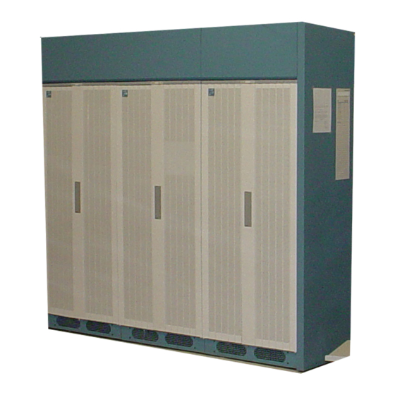
- Page 21 Super J-Drawing.) The Peripheral Growth Cabinets are always located to the right of the Processor Cabinet, as viewed from the front of the cabinets. The cabinets each measure about 72 inches (183 cm) high by 30 inches (76 cm) wide by 24 inches (60 cm) deep. Copyright © 1999 Lucent Technologies Page 1...
- Page 22 The initial (basic) system configuration consists of the Processor Cabinet equipped with the following major units: One Modular Filter and Fuse Panel Unit, J5D003FJ-1 One Bidirectional Cooling Unit, J5D003FH-2 Two Processor Units, J3T060AA-1. Copyright © 1999 Lucent Technologies Page 2...
- Page 23 1; two of the Growth Unit SPUs are connected to DFC 0, SBUS 0. See Table 3-1 for SPU controller and bus assignments. NOTE: DFC 0 and DFC 1 could be equipped with either a UN580 or with both a TN2116 and a UN373. OP 0 with Peripheral Communities 0, 1, 2, and 3. Copyright © 1999 Lucent Technologies Page...
- Page 24 OP 0 with Peripheral Communities 0, 1, 2, and 3. OP 1 with Peripheral Communities 0, 1, 2, and 3. OP 2 with Peripheral Communities 0 and 1. OP 3 with Peripheral Communities 0 and 1. Copyright © 1999 Lucent Technologies Page 4...
- Page 25 2 5-105-510 July 1999 Figure -2 Processor Cabinet, J T060A-1 Basic System Configuration, Front View Copyright © 1999 Lucent Technologies Page 5...
- Page 26 2 5-105-510 July 1999 Copyright © 1999 Lucent Technologies Page 6...
- Page 27 2 5-105-510 July 1999 Figure - Processor Cabinet, J T060A-1 Configuration Example 1, Front View Copyright © 1999 Lucent Technologies Page 7...
- Page 28 2 5-105-510 July 1999 Copyright © 1999 Lucent Technologies Page 8...
- Page 29 .2.7 Peripheral Growth Cabinet, J T059A-1 Configuration Example 4 Configuration Example 4 for the Peripheral Growth Cabinet provides the fourth SCS 9-track tape drive, KS-23909 (SPU58) in the second Peripheral Growth Cabinet. See Figure 3-8 for equipage information. Copyright © 1999 Lucent Technologies Page 9...
- Page 30 2 5-105-510 July 1999 Copyright © 1999 Lucent Technologies Page 10...
- Page 31 2 5-105-510 July 1999 Figure -5 Peripheral Growth Cabinet, J T059A-1 Configuration Example 1, Front View Copyright © 1999 Lucent Technologies Page 11...
- Page 32 2 5-105-510 July 1999 Copyright © 1999 Lucent Technologies Page 12...
- Page 33 2 5-105-510 July 1999 Figure -6 Peripheral Growth Cabinet, J T059A-1 Configuration Example 2, Front View Copyright © 1999 Lucent Technologies Page 1...
- Page 34 2 5-105-510 July 1999 Copyright © 1999 Lucent Technologies Page 14...
- Page 35 2 5-105-510 July 1999 Figure -7 Peripheral Growth Cabinet, J T059A-1 Configuration Example , Front View Copyright © 1999 Lucent Technologies Page 15...
- Page 36 2 5-105-510 July 1999 Copyright © 1999 Lucent Technologies Page 16...
- Page 37 DFC 1/SBUS 1 DFC 1/SBUS 1 DFC 1/SBUS 1 SPU06 19-154 DFC 0/SBUS 2 SPU07 45-154 DFC 1/SBUS 3 SPU08 28-118 DFC 0/SBUS 0 SPU09 53-118 DFC 1/SBUS 1 SPU10 19-138 DFC 0/SBUS 2 Copyright © 1999 Lucent Technologies Page 17...
- Page 38 DFC 0-1/ DFC 0-1/ DFC 0-1/ (9-TRACK2) SBUS 0-3 SBUS 0-3 SBUS 0-3 Notes: An SPU can be any SCS device such as 9-track tape, DAT, MHD drive, or magnetic tape (MT) unit. Copyright © 1999 Lucent Technologies Page 18...
- Page 39 Figure 4-1 shows the unit equipage of the Processor Cabinet and the two Peripheral Growth Cabinets. Figure 4-2 provides a general equipment configuration overview of the Processor Cabinet. The front doors of the cabinets are not shown in these figures. Figure 4-1 B21D Computer System Cabinets Front View Copyright © 1999 Lucent Technologies Page 1...
- Page 40 2 5-105-510 July 1999 Copyright © 1999 Lucent Technologies Page 2...
- Page 41 2 5-105-510 July 1999 Copyright © 1999 Lucent Technologies Page...
-
Page 42: Figure 4-2 Processor Cabinet Equipment Overview Front View
Figure 4-3 shows apparatus housing layout details for the Processor Units 0 and 1. Table 4-1 identifies the equipage of the Processor Unit 0 and Processor Unit 1 in the Processor Cabinet. Figure 4- Processor Unit, J T060AA-1 Equipment Layout, Front View Copyright © 1999 Lucent Technologies Page 4... - Page 43 Two Growth Units can be equipped in the Processor Cabinet. Figure 4-4 shows apparatus housing layout details for the Growth Units. Table 4-2 identifies the equipage of the OP 2-SPU and OP 3-SPU Growth Units in the Processor Cabinet. Copyright © 1999 Lucent Technologies Page 5...
- Page 44 Equipage is PC10 (RED) 62-072 PC11 (RED) 62-080 PC10 (RED) 11-072 application PC11 (RED) 11-080 PC12 (RED) 62-088 dependent PC13 (RED) 62-096 PC12 (RED) 11-088 PC13 (RED) 11-096 and includes peripheral Copyright © 1999 Lucent Technologies Page 6...
- Page 45 Equipage is application SPU 18 11-180 SPU 19 62-180 dependent and includes SCS peripheral units. 4.2. Modular Fuse and Filter Unit, J5D00 FJ-1 Figure 4-5 shows the fuse assignments for the Processor Cabinet. Copyright © 1999 Lucent Technologies Page 7...
- Page 46 2 5-105-510 July 1999 Copyright © 1999 Lucent Technologies Page 8...
- Page 47 2 5-105-510 July 1999 Copyright © 1999 Lucent Technologies Page 9...
-
Page 48: Figure 4-5 Processor Cabinet Fuse Assignments
The Printed Wiring Board (PWB) general characteristics are summarized in Table 4-3 for the UN, TN, KLW, and ® KBN circuit pack types. All PWBs are manufactured per Fastech electronic packaging system standards. See the Copyright © 1999 Lucent Technologies Page 10... - Page 49 C-24589 B-01367 13-088 410AA Power Converter D C-24589 B-01367 13-188 410AA Power Converter E C-24589 B-13678 13-170 TN2116 SCS Host Adapter C-02459 B-02368 04-038 KLW31 CC C-14579 B-02457 04-018 EX 0 Slot C-13689 Copyright © 1999 Lucent Technologies Page 11...
-
Page 50: Table 4-5 Growth Unit Backplane Keys
C-01234 B-56789 04-108 PC20 C-01234 B-56789 04-116 PC21 C-01234 B-56789 04-124 PC22 C-01234 B-56789 04-132 PC23 C-01234 B-56789 04-140 PC30 C-01234 B-56789 04-148 PC31 C-01234 B-56789 04-156 PC32 C-01234 B-56789 04-164 PC33 C-01234 Copyright © 1999 Lucent Technologies Page 12... -
Page 51: Figure 4-6 Backplane Key Holder
2 5-105-510 July 1999 Figure 4-6 Backplane Key Holder 4.6 OPTIONAL CIRCUIT PACKS AND MODULES 4.6.1 UN 79 Utility Circuit (UC) Circuit Pack Copyright © 1999 Lucent Technologies Page 1... - Page 52 Table 4-6 CC Interrupt Inputs CC PIN CC SIGNAL NAME EXTERNAL INTERRUPT FIELD DESCRIPTION 044T S S150 NC a 045T S S140 Copyright © 1999 Lucent Technologies Page 14...
- Page 53 4.9.1 Design Characteristics The cabling design follows the following guidelines: All internal ribbon cabling is twisted pair to minimize electromagnetic noise. Total cable length for differential SCS bus does not exceed 25 meters. Copyright © 1999 Lucent Technologies Page 15...
- Page 54 Three fans are in each group. The fan motors operate on -48 V DC. One group blows air upward to cool Processor 1 and OP 3-SPU Growth Unit; the other group blows downward to cool Processor 0 and OP 2-SPU Growth Unit. Copyright © 1999 Lucent Technologies Page 16...
- Page 55 Board-Mounted Power Module (BMPM) in the alarm circuit. f one or more fans fail, the circuit latches an alarm state on its scan point output. The SD point is used to retire the alarm. A switch on the cooling unit can also be used to manually retire the alarm. Copyright © 1999 Lucent Technologies Page 17...
- Page 56 One UC circuit pack (UN379) is optionally equipped in each CU. 5.1.1.4 Cache Storage Unit (CSU) The CSU provides a small, high-speed CC cache memory for the most recently accessed Main Store (MAS) words. Copyright © 1999 Lucent Technologies Page 1...
- Page 57 3B21D computer DFC channel and device allocations differ from the 3B20D computer in that there are fewer devices per channel. 5.1.2.1 Disk File Controller (DFC) The 3B21D computer can have three DFCs (DFC 0 through DFC 2) all equipped in the Processor Cabinet as follows: Copyright © 1999 Lucent Technologies Page 2...
- Page 58 One port switch is equipped in Processor Unit 1. n the 3B21D computer, the PSSBD is located in CU 1. (Note that in the 3B20D computer the PSSBD is located in CU 0.) Copyright © 1999 Lucent Technologies Page...
- Page 59 2 5-105-510 July 1999 Figure 5-1 B21D Computer Functional Block Diagram 5.2 CENTRAL CONTROL (CC) Copyright © 1999 Lucent Technologies Page 4...
- Page 60 Store Address Translator (SAT) Cache Storage Unit (CSU) Micro Level Test Set (MLTS) nterface. Following a description of the CC interfaces, each of these functions is described in this section. Copyright © 1999 Lucent Technologies Page 5...
-
Page 61: Figure 5-2 Central Control (Cc) Functional Block Diagram
2 5-105-510 July 1999 Figure 5-2 Central Control (CC) Functional Block Diagram 5.2.1 CC Interfaces 5.2.1.1 Central Control I/O (CCIO) Bus Copyright © 1999 Lucent Technologies Page 6... - Page 62 D0 NT10 DMAC 0 Channel 1 nterrupt nterrupt summary for application peripherals D1 NT00 DMAC 1 Channel 0 nterrupt nterrupt summary for 3B21D peripherals D1 NT10 DMAC 1 Channel 1 nterrupt nterrupt summary for Copyright © 1999 Lucent Technologies Page 7...
- Page 63 5.2.1.1.1 CCIO Data Bus The CC O data (CC OD) bus is 32-bit bus. The bus connects the DMAC to the Channel Data Register (CDR) on the CC circuit pack. 5.2.1.1.2 CCIO Data Parity Copyright © 1999 Lucent Technologies Page 8...
- Page 64 CC Error Register bit 16. This triggers an error interrupt in the CC. All-Seems-Well (CIOASW0) The All-Seems-Well signal indicates the absence of errors. ts status is stored in HSR bit 4. An All-Seems-Well failure asserts the CC Error Register bit 17. Ready (CIORDY0) Copyright © 1999 Lucent Technologies Page 9...
- Page 65 (MAS) and Main Store Update (MASU)" in Section 6 . Table 5-4 Main Store Bus CATEGORY SIGNAL TYPE DESCRIPTION DMA0/1 EX0/1 DATA SD(31-00)1 Tri a 32 noninverted SD(35-32)1 Bid a 4-byte even parity bits over 32 Copyright © 1999 Lucent Technologies Page 10...
- Page 66 Other store access time-out SCR161 Cache Go Signal SCR251 Arbiter reset CACWT0 MM waits for invalidate CLER150 Clear Other store access time-out CPWRCLR0 Power-up clear Notes: Tri = Tristate; Bid = Bidirectional; Uni = Unidirectional. Copyright © 1999 Lucent Technologies Page 11...
- Page 67 2 5-105-510 July 1999 NC = No Connection. Copyright © 1999 Lucent Technologies Page 12...
-
Page 68: Figure 5-4 Main Store Bus Functional Block Diagram
2 5-105-510 July 1999 Figure 5-4 Main Store Bus Functional Block Diagram Copyright © 1999 Lucent Technologies Page 1... -
Page 69: Figure 5-5 Maintenance Channel Link (Mchl) Protocol
CLKAN RS-422 Serial link clock output, negative phase REQAP RS-422 Link stop and switch interrupt, positive phase REQAN RS-422 Link stop and switch interrupt, negative phase Figure 5-5 Maintenance Channel Link (MCHL) Protocol Copyright © 1999 Lucent Technologies Page 14... -
Page 70: Figure 5-6 Maintenance Channel Link (Mchl) Functional Block Diagram
Figure 5-6 Maintenance Channel Link (MCHL) Functional Block Diagram 5.2.1.4 CC to MLTS Link The Micro Level Test Set (MLTS) link connects the MLTS host and the MLTS interface circuits. Figure 5-7 is a functional block diagram of the MLTS link. Copyright © 1999 Lucent Technologies Page 15... -
Page 71: Figure 5-7 Micro Level Test Set (Mlts) Link Functional Block Diagram
MCH loads the idle value (0X00) between legal values to prevent simultaneous multiple ring accesses. The 8-bit register is loaded via the MCH. Table 5-6 lists the 8-bit codes used to select the BS rings. Table 5-6 Boundary Scan Ring Selection Register Codes Copyright © 1999 Lucent Technologies Page 16... - Page 72 All boundary scan operations are controlled by the CC; however, additional circuitry is provided by the nput/Output Processor Power Switch ( OPPS) circuit pack (TN1820) for access to the secondary and growth buses. Copyright © 1999 Lucent Technologies Page 17...
-
Page 73: Figure 5-8 Typical Boundary Scan (Bs) Bus Functional Block Diagram
Maintenance Channel (MCH). The active CU instructs the MCH on the inactive CU to scan for self-identification data. The KBN10 OP self-identification EPROM is read via the dual Copyright © 1999 Lucent Technologies Page 18... - Page 74 The boundary scan bus is routed to the DFCB position. The current DFCB circuit pack (TN2116) does not support boundary scan. The port is routed to pin fields not used by the TN2116, allowing any future circuit packs that may be installed here to support boundary scan, if desired. Copyright © 1999 Lucent Technologies Page 19...
- Page 75 2 5-105-510 July 1999 Copyright © 1999 Lucent Technologies Page 20...
-
Page 76: Figure 5-9 Boundary Scan (Bs) Functional Block Diagram
2 5-105-510 July 1999 Figure 5-9 Boundary Scan (BS) Functional Block Diagram Copyright © 1999 Lucent Technologies Page 21... -
Page 77: Figure 5-10 Boundary Scan Circuit Pack Access
MLTRW0 WMS access direction by MLTS HSR (23-16) BGB sources, destinations, direction, and enable PPR (21-16) Pulse point register bits 21-16 for BGB accesses Notes: NC = No Connection. Copyright © 1999 Lucent Technologies Page 22... - Page 78 2 5-105-510 July 1999 Copyright © 1999 Lucent Technologies Page 2...
-
Page 79: Figure 5-11 Bidirectional Gating Bus (Bgb) Functional Block Diagram
5-bit code, and combine the results with the master clock to control the CC registers in each AS C. For some AS Cs, this decoding is done in the MSEQ and individual DST clocks are sent to the AS C to save pins on the Copyright © 1999 Lucent Technologies Page 24... -
Page 80: Table 5-8 Source (Src) And Destination (Dst) Buses
Source enable 21 A SRCEB210 Unidirectional Source enable 21 B SRCEBA10 Unidirectional Source enable 1 BA SRCEBA30 Unidirectional Source enable 3 BA SRCEBB10 Unidirectional Source enable 1 BB SRCEBB30 Unidirectional Source enable 3 BB Copyright © 1999 Lucent Technologies Page 25... -
Page 81: Figure 5-12 Source (Src) And Destination (Dst) Bus Functional Block Diagram
2 5-105-510 July 1999 Figure 5-12 Source (SRC) and Destination (DST) Bus Functional Block Diagram 5.2.2.4 Maintenance (MTC) Bus Copyright © 1999 Lucent Technologies Page 26... - Page 82 MTC(35-32)1 Tristate, 4-byte even parity bits bidirec- over 32 data bits tional CONTROL MTCEN(1-0)1 Open MTC bus source enable Collector MTCSL(1-0)1 Open MTC bus source select Collector Notes: NC = No Connection. Copyright © 1999 Lucent Technologies Page 27...
- Page 83 Table 5-10 summarizes the cache memory bus. Table 5-10 Cache Memory Bus CATEGORY SIGNAL TYPE DESCRIPTION DATA CD(31-00)1 Tristate 32 data bits, noninverted NC a CDP(35-32)1 Bidirec- tional 4-byte even parity bits over 32 data Copyright © 1999 Lucent Technologies Page 28...
- Page 84 Verifies the contents of the M R by comparing its parity result with the Micro nstruction parity bits. Maintains an 8-word deep, wrap-around Micro nstruction return address stack. Copyright © 1999 Lucent Technologies Page 29...
- Page 85 The SDR can be loaded from the DST bus or from the MAS bus. Similarly, the SDR can be read from the SRC bus or placed onto the MAS bus. The Store nstruction Register (S R) contains the next macroinstruction fetched from the MM. The S R can also Copyright © 1999 Lucent Technologies Page 0...
- Page 86 (SD ), Cache Storage Unit (CSU), and Main Memory (MM) during CC memory accesses. The SSEQ coordinates MM accesses. 5.2.7 Store Address Translator (SAT) The Store Address Translator (SAT) function is provided by the SAT AS C, a set of MASB buffers, and a set of Copyright © 1999 Lucent Technologies Page 1...
- Page 87 The CSU increases CC performance by reducing the average main memory access time. t provides two distinct high-speed memory functions as follows: A direct-mapped data and instruction cache memory A high-speed interrupt stack memory. Copyright © 1999 Lucent Technologies Page 2...
- Page 88 The FLZ logic identifies the bit position of the first zero found from the least significant end of the data word or source register. The Bypass ALU logic transfers data from the SRC bus to the DST bus without any manipulation. Copyright © 1999 Lucent Technologies Page...
- Page 89 The MTC bus is used to verify the proper operation of the processor. The TR provides a Sanity Timer, nterrupt Timer ( T), and prescalars for the RTC and T. The CC O backplane interface is provided. This interface includes data, address, and control signals. Copyright © 1999 Lucent Technologies Page 4...
- Page 90 All other bits can be written and read. The HSR is loaded from the DST bus (except for the read-only bits), and read via the source bus and the destination bus. The HSR bits are summarized in Table 5-11 . Copyright © 1999 Lucent Technologies Page 5...
- Page 91 2 5-105-510 July 1999 Figure 5-14 Special Registers Functional Block Diagram Copyright © 1999 Lucent Technologies Page 6...
-
Page 92: Table 5-11 Hardware Status Register (Hsr) Bit Layout
Set write PSW (bit 23), set /O (bit 22), set maintenance (bit 21), and set execution (bit 20) privilege (permission) bits. 27-24 nterrupt execution level for fetching nterrupt Mask ( M) value. 31-28 Software controlled bits. Copyright © 1999 Lucent Technologies Page 7... -
Page 93: Table 5-14 System Status Register (Ssr) Bit Layout
Signal Power Clear (bit 15), "This CC On-Line" (bit 16), and halt mode (bit 17). Block S interrupts when = 0 (Non-asserted on power up). n update mode when = 0. 21-20 solate DMA (bit 20) and other CC (bit 21). solate Expansion Slot. Copyright © 1999 Lucent Technologies Page 8... - Page 94 Source register. f a bit in the S is set and the corresponding bit in the M is cleared, an interrupt signal is generated. The S is read via the SRC bus. 5.2.10.8 Channel Data Register (CDR) Copyright © 1999 Lucent Technologies Page 9...
-
Page 95: Table 5-16 Timer Register (Tr) Bit Layout
MCH receives this interrupt, it activates its MRF0 output, which causes the other processor to go on-line. f the other processor is already on-line, and not disabled, the receiving MCH does not activate MRF0. nstead, an error is recorded. Copyright © 1999 Lucent Technologies Page 40... - Page 96 MCH only uses 2 K of address space. The differential signals in the MCHL are converted by the RS-422 circuitry to logic signals for the MCH. The 64-bit MSD bus is multiplexed and requires the external registers. The BSM interface Copyright © 1999 Lucent Technologies Page 41...
-
Page 97: Table 5-17 Maintenance Channel (Mch) Signals
Figure 5-15 Maintenance Channel (MCH) Functional Block Diagram Table 5-17 Maintenance Channel (MCH) Signals CATEGORY SIGNAL TYPE DIRECTION DESCRIPTION M CROSTORE BUS MSD(63-00)1 Tristate MicroStore Data bus, multiplexed 32 data (MSA, MSB) bits. Copyright © 1999 Lucent Technologies Page 42... - Page 98 Serial link clock output, positive phase. CLKAN RS-422 Serial link clock output, negative phase. TXEN0 Enable external DAHA and DALA RS-422 drivers. RXEN0 Enable external DAHA and DALA RS-422 receivers. REQAP RS-422 Link stop and switch interrupt, positive Copyright © 1999 Lucent Technologies Page 4...
- Page 99 Port control and status register. BSMRD BSM Port Read. BSM NT BSM Port nterrupt. BSMSELCLK Boundary scan chain selector clock. BSMTCLK BSM Timing Clock references supplied to the BSM by the MCH. 5.2.11.1 MCH BGB Interface Copyright © 1999 Lucent Technologies Page 44...
-
Page 100: Table 5-18 Maintenance Channel (Mch) Control Signals
"sendsw" master command. When the STPSW0 approach is used, the resulting REQAOUT interrupt from the MCH is used with the STPSW0 signal to automatically set the STOP flipflop. When a master command is used, the processor must stop itself. 5.2.11.7 Maintenance Reset Function Copyright © 1999 Lucent Technologies Page 45... - Page 101 Disable Sanity Timer (DT M) Forces the associated CC sanity timer to be disabled, thus inhibiting subsequent switches if software execution is abnormal. Table 5-20 EAI Initialization Functions Copyright © 1999 Lucent Technologies Page 46...
- Page 102 Output EA Status (OUTSTAT) Transfers a status message to the MTTYC. Output PRM (OUTPRM) Transfers the 64-bit Processor Recovery Message (PRM) output buffer to the MTTYC. Figure 5-16 Emergency Action Interface (EAI) Functional Block Diagram Copyright © 1999 Lucent Technologies Page 47...
- Page 103 DEFINITION The latch is cleared by a read operation. Bit values are "don't cares." Table 5-22 EAI Normal Pulse Point Functions B21D COMPUTER NORMAL EAI PULSE-POINT INTERRUPTS PPR2 PPR22 PPR11 FUNCTION No nterrupt. Copyright © 1999 Lucent Technologies Page 48...
- Page 104 Move PRM 0 Output Buffer to P Buffer MVOB10 Move PRM 1 nput Buffer to P Buffer MVOB11 Move PRM 1 Output Buffer to P Buffer MV NST Move nput Status to P Buffer Copyright © 1999 Lucent Technologies Page 49...
- Page 105 EAI Error Register DEFINITION Emergency Action Output Error DUART Self-test Loopback Failure DUART Self-test nitialization Failure EPROM Self-test Checksum Failure SRAM Self-test/Diagnostic Failure Unexpected Software nterrupt Sanity Timeout SRAM Parity Error 5.2.12. EAI EPROM Copyright © 1999 Lucent Technologies Page 50...
- Page 106 Displays the state of the Emergency Action Enabled (EAEN) status bit of the EA . Lights ACT ON (amber) when a force function to the 3B21D computer is active or when the nitialization Copyright © 1999 Lucent Technologies Page 51...
- Page 107 Clear and set provides the capability of clearing (negating) or setting (asserting) a number of important CC bits or registers such as Panel nterrupt, STOP bit, Sanity Timer, Disable bit, and the Error register. Copyright © 1999 Lucent Technologies Page 52...
- Page 108 2 5-105-510 July 1999 Figure 5-17 Micro Level Test Set Interface Functional Block Diagram Copyright © 1999 Lucent Technologies Page 5...
- Page 109 2 5-105-510 July 1999 Copyright © 1999 Lucent Technologies Page 54...
- Page 110 Update Bus cabling. These four CC signals are not connected with any logic in the MM circuit pack but enable the two processors to communicate if the regular Maintenance Channel has failed. Table 6-1 summarizes the Update Bus signals. Copyright © 1999 Lucent Technologies Page 1...
- Page 111 2 5-105-510 July 1999 Figure 6-1 Main Memory (MM) Functional Block Diagram Table 6-1 Update Bus CATEGORY SIGNAL TYPE DIRECTION DESCRIPTION Copyright © 1999 Lucent Technologies Page 2...
- Page 112 Other Store Error C (negative) SUOERRCP Other Store Error C (positive) SUOERRDN Differential Other Store Error D (negative) SUOERRDP Other Store Error D (positive) BACKUP POD SAN Differential Pulse Point Register bit 14 to other side Copyright © 1999 Lucent Technologies Page...
- Page 113 The following list of DRAM control signals provide the correct timing protocol to the DRAM devices: Data Address Row Address Strobe (RAS) Column Address Strobe (CAS) Write Enable (WE) Output Enable (OE). Copyright © 1999 Lucent Technologies Page 4...
- Page 114 (for example, quad word, half word, or full word) and assumes even parity. This affects byte 3 where bits 0 and 1 are not used. Registers in the MC mode determine the following: Refresh interval/generation Page mode length Copyright © 1999 Lucent Technologies Page 5...
- Page 115 These signals are Store Go, Abus, Dbus, Data Strobe, and Store CoMplete. The functional hardware accepts requests, arbitrates to provide the six possible Copyright © 1999 Lucent Technologies Page 6...
- Page 116 My Store Errors to the other store through the Update Bus [SUERR(A,B,C,D)]. The other store passes these signals to its SREG [OSTER(A,B,C,D)]. My Store also receives the Other Store Errors [SUOERR(A,B,C,D)] and sends them to the SREGs [OSTER(A,B,C,D)]. 6.1.6 Self-Identification (SLFID) Circuit Copyright © 1999 Lucent Technologies Page 7...
- Page 117 PPR14 and PPR15 in the active processor. This is done by the software when it deems vital to reset the other processor and the regular maintenance channel is determined to be not working. Copyright © 1999 Lucent Technologies Page 8...
- Page 118 36-bit word blocks. nterfaces with the CC through the CC O bus. The CC performs programmed /O (P O) operations to the DMAC, the channels, and the peripheral devices through this interface. Copyright © 1999 Lucent Technologies Page 9...
- Page 119 2 5-105-510 July 1999 Figure 6- Direct Memory Access (DMA) Functional Block Diagram 6.2.1 Direct Memory Transfers The DMAC Main Memory nterface implements the 3B21D computer MASB protocol and controls full and quad word Copyright © 1999 Lucent Technologies Page 10...
- Page 120 Bit 30 enables internal bus parity checking. Bits 34-31 contain the 2910 device instructions. Bits 39-35 contain the 5 parity bits across the 5 bytes that make up the 40-bit word. Copyright © 1999 Lucent Technologies Page 11...
- Page 121 The SLF D circuit provides the means for a Central Control (CC) to interrogate the DMA circuit pack for identification information (version, issue, and so forth). The circuit operates independently from the DMAC/DSCH AS C. Copyright © 1999 Lucent Technologies Page 12...
- Page 122 Provide four triggers that can accept input from any matcher or combination of matchers and generate an interrupt. Record Trace Memory, which is controlled by the Trigger Function outputs. The Trace Memory can record until Copyright © 1999 Lucent Technologies Page 1...
- Page 123 Transfers, U D Changes, Function Calls, and Function Returns. n addition, any of these program trace modes can be used simultaneously with Data History Trace. Figure 6-4 Utility Circuit (UC) Functional Block Diagram Copyright © 1999 Lucent Technologies Page 14...
- Page 124 U D Map using BGBPP(2)0. When a nonsequential access occurs (BRANCH0 is active), the new value of TAA(10-08) is compared to the old value. An indication of any U D change is output to the Trigger Logic, which decides if a trigger function should be enabled. Copyright © 1999 Lucent Technologies Page 15...
- Page 125 The Expansion Slots (EX 0 and EX 1) provide an interface for new hardware features to access the MAS and for the CC to access the new hardware through the CC O bus or the MASB. Copyright © 1999 Lucent Technologies Page 16...
- Page 126 When a DFC is equipped with a UN580B, the UN580B installs in the slot previously used for a UN373 or UN580. There is an unused circuit pack position on both sides of a UN580B. Copyright © 1999 Lucent Technologies Page 1...
- Page 127 7.1.4 Small Computer System Interface (SCSI) The SCS portion of the HA controls data transfers between two independent SCS buses and the rest of the HA. The specific functions of the SCS are as follows: Copyright © 1999 Lucent Technologies Page 2...
- Page 128 The UN580 circuit pack does not have any self-identification functionality. The self-identification function was put back on the UN580B; however (like the UN373), the circuit components are not installed. Copyright © 1999 Lucent Technologies Page...
- Page 129 2 5-105-510 July 1999 Copyright © 1999 Lucent Technologies Page 4...
- Page 130 Figure 7-2 is a functional block diagram of the OP circuit pack (KBN10). The OP consists of the following functional blocks: Duplex Dual Serial Bus Selector (DDSBS) Bus nterface Controller (B C) Peripheral nterface Controller (P C) Copyright © 1999 Lucent Technologies Page 5...
- Page 131 2 5-105-510 July 1999 nput/Output Microprocessor nterface ( OM ). Each of these functional areas is described in the following sections. Copyright © 1999 Lucent Technologies Page 6...
- Page 132 2 5-105-510 July 1999 Figure 7-2 Input/Output Processor Functional Block Diagram Copyright © 1999 Lucent Technologies Page 7...
- Page 133 PC select lead. Each community of four PCs share an 8-bit plus 1 parity bit data bus, a 16-bit memory address bus, and an 8-bit bus containing control signals. Copyright © 1999 Lucent Technologies Page 8...
- Page 134 Processor Unit and is via the growth boundary scan cable when equipped in the Growth Unit. The BS bus is a serial bus used to test (diagnose) components. All boundary scan functions are controlled by the CC. PERIPHERAL CONTROLLERS (PC) The 3B21D computer supports the following peripheral controllers: Copyright © 1999 Lucent Technologies Page 9...
- Page 135 (Maximum) 9600 960+0 9600 0+960 4800 4800 480+480 7. .2 TN75C Synchronous Data Link Controller The TN75C circuit pack provides two independent X.25 level 2 interfaces (channel 0 and channel 1), with automatic Copyright © 1999 Lucent Technologies Page 10...
- Page 136 45-094-022, that must be isolated for the UN583/UN597 to operate. f you are retrofitting a UN583 or UN597 in place of a TN983 on an older backplane, make sure these two pins are isolated. The UN583/UN597 will not operate if these two pins are not isolated. Copyright © 1999 Lucent Technologies Page 11...
- Page 137 SDLC, HDLC, and ADCCP. The channel provides the necessary control signals that meet the E A RS-232C interface standard for data rates up to 19.2 Kbps and CC TT V.36 interface for Copyright © 1999 Lucent Technologies Page 12...
- Page 138 SD points are activated by commands from the CU. Only one point at a time may be activated or deactivated. SD points can be directed by the CU to any of four states: Operate Clear Copyright © 1999 Lucent Technologies Page 1...
- Page 139 Closed if ROP select switch is set to automatic (AUTO). SCA56 Closed when the UN377 has power. SCB56 Closed if MTTY output is from MTTYPC0. (Duplicates SCA40.) SCC56 Closed if MTTY select switch is set to AUTO. Copyright © 1999 Lucent Technologies Page 14...
- Page 140 Digital Audio Tape (DAT), one MTTY, one ROP, a Bidirectional Cooling Unit, and a Fuse and Filter Unit is 42 SC points and 32 SD points. n addition, eight SD points (four SD points per base UN33 or UN933 circuit pack) are Copyright © 1999 Lucent Technologies Page 15...
- Page 141 Y(POWER) OP 1 X(ROS/RST) RQ P OP 0 X(ROS/RST) RQ P SPU 02 X(ROS/RST) SPU 03 X(ROS/RST) SPU 02 Y(POWER) RQ P SPU 03 Y(POWER) RQ P SPU 00 X(ROS/RST) SPU 01 X(ROS/RST) Copyright © 1999 Lucent Technologies Page 16...
- Page 142 SPU 05 Y (POWER) RQ P OP 2 Y (POWER) OP 3 Y (POWER) OP 2 X (ROS/RST) RQ P OP 3 X (ROS/RST) RQ P OP 1 Y (POWER) OP 0 Y (POWER) Copyright © 1999 Lucent Technologies Page 17...
- Page 143 (RC/V) mechanism. To determine logical and physical scan point assignments using the RC/V mechanism, use the following procedure. At the recent change terminal, enter the following: PDS RCV:MENU:RCVECD,DB "root",NREVIEW! Copyright © 1999 Lucent Technologies Page 18...
- Page 144 REPEAT flash continuously. To verify operation of the selected SD point, use the ORD:SCSD message to flash the point while observing the state of associated lamps and indicators. Typical SD Point Verification Example Copyright © 1999 Lucent Technologies Page 19...
- Page 145 "A" switch; the ROP is controlled by the "B" switch. Figure 7-6 shows the layout of the UN377 circuit pack faceplate. Table 7-7 defines the UN377 switch positions. Table 7-8 defines the UN377 indicators. Copyright © 1999 Lucent Technologies Page 20...
- Page 146 2 5-105-510 July 1999 Figure 7-5 Port Switch and Scanner-Distributor Buffer (PSSDB) Functional Interface Diagram Copyright © 1999 Lucent Technologies Page 21...
- Page 147 2 5-105-510 July 1999 Copyright © 1999 Lucent Technologies Page 22...
- Page 148 Module (BMPM). The BMPM is supplied -48 V from the Modular Fuse and Filter Unit. The UN377 includes a voltage monitor that checks the circuit pack +5 V power. When the +5 V power is out of range, the voltage monitor generates a power alarm. Copyright © 1999 Lucent Technologies Page 2...
- Page 149 D pushbutton switch. NOTE: Set the SCS D for the UN375/UN375E circuit pack when the circuit pack is powered OFF. The SCS D will take effect when the circuit pack is powered ON. Copyright © 1999 Lucent Technologies Page 1...
- Page 150 Note that different SCS D connectors are provided for the KS-23908,L20 disk drive and KS-23908,L10 disk drive SCS D headers as shown in Figure 8-3 . Only one of these SCS D connectors is used, depending on which disk drive is used in the circuit pack. Copyright © 1999 Lucent Technologies Page 2...
- Page 151 2 5-105-510 July 1999 Copyright © 1999 Lucent Technologies Page...
- Page 152 2 5-105-510 July 1999 Figure 8-1 UN 75/UN 75E Circuit Pack Faceplate Figure 8-2 UN 75/UN 75E (KS-2 908) .5-Inch Hard Disk Drive Rear View Copyright © 1999 Lucent Technologies Page 4...
- Page 153 The system is configured to either have all SCS devices generate and detect parity or no devices generate and detect parity. Parity is not valid during the Arbitration phase. +D FFSENS Positive Differential Sense. 22-24 Ground Copyright © 1999 Lucent Technologies Page 5...
- Page 154 True (active) indicates input to the initiator. The signal is also used to distinguish between Selection and - /O Reselection phases. 8.2.2 UN 75/UN 75E Functional Description Copyright © 1999 Lucent Technologies Page 6...
- Page 155 -48 V is lost and the alarm cutoff-test (ACO-T) switch is off. The MJ is cleared when power is reapplied. The POWER ALARM is generated when either ALM50 or ALM120 alarms are present and -48 V is present (ON). The POWER ALARM is independent of the position of the ACO-T switch. Copyright © 1999 Lucent Technologies Page 7...
- Page 156 2 5-105-510 July 1999 Copyright © 1999 Lucent Technologies Page 8...
- Page 157 +12 V converter or the other +5 V converter fails, the power control and alarm circuits will still operate to Copyright © 1999 Lucent Technologies Page 9...
- Page 158 DDS logo meet the requirements of the European Computer Manufacturers Association (ECMA-130) and ANS X3.206 standards. The usable storage capacity provided by the DAT drive varies with the length of tape and the recording mode. Table Copyright © 1999 Lucent Technologies Page 10...
- Page 159 An ALM indicator cable connects the ALM indicator header (J6) on the circuit board and the ALM indicator on the faceplate. A Request-Out-of-Service/Restore (ROS/RST) switch cable connects the ROS/RST switch header (J7) on the circuit board and the ROS indicator on the faceplate. Copyright © 1999 Lucent Technologies Page 11...
- Page 160 An SCS identification cable connects the SCS D switches SW8-SW6 on the circuit board (via J9, a 6-pin header) and the SCS D header on the DAT drive (via a paddleboard). Copyright © 1999 Lucent Technologies Page 12...
- Page 161 2 5-105-510 July 1999 Copyright © 1999 Lucent Technologies Page 1...
- Page 162 Error Hard fault. Flash Green Cleaning Cleaning cartridge is in process of loading, unloading, or cleaning. Notes: Flash = ¼ second ON, ¼ second OFF; Pulse = ½ second ON, ½ second OFF. Copyright © 1999 Lucent Technologies Page 14...
- Page 163 2 5-105-510 July 1999 Copyright © 1999 Lucent Technologies Page 15...
- Page 164 2 5-105-510 July 1999 Copyright © 1999 Lucent Technologies Page 16...
- Page 165 True (active) indicates input to the initiator. The signal is also used to distinguish between Selection and Reselection phases. Copyright © 1999 Lucent Technologies Page 17...
- Page 166 Closed (1) Open (0) Open (0) Closed (1) Open (0) Closed (1) Closed (1) Closed (1) Open (0) Closed (1) Closed (1) Closed (1) Notes: SCS device D number 7 is not allowed. Copyright © 1999 Lucent Technologies Page 18...
- Page 167 2 5-105-510 July 1999 Copyright © 1999 Lucent Technologies Page 19...
- Page 168 Power switch circuit providing power control, power alarm, scan point, and signal distributor point functions +12 V power supply +5 V power supply NCR006-3503341, NCR006-3300608/Comcode 407545243 (UN376C), or KS-24367,L1/Comcode 407771260 (UN376E) single-ended SCS , 3.5-inch DAT drive Copyright © 1999 Lucent Technologies Page 20...
- Page 169 -48 V is lost and the ACO-T switch is off. The MJ is cleared when power is reapplied. The POWER ALARM is generated when either ALM50 or ALM120 alarms are present and -48 V is present (ON). The POWER ALARM alarm is independent of the position of the ACO-T switch. Copyright © 1999 Lucent Technologies Page 21...
- Page 170 2 5-105-510 July 1999 Copyright © 1999 Lucent Technologies Page 22...
- Page 171 8. .2. . JW0 0A +5 V Board-Mounted Power Module The JW030A +5 V board-mounted power module is a 30-watt DC-to-DC converter that operates from -48 V DC and Copyright © 1999 Lucent Technologies Page 2...
- Page 172 These states do NOT directly relate to the state of the drive and cassette indicators defined in Table 8-7 . Table 8-14 NCR006- 50 41 DAT States STATE DEFINITION Copyright © 1999 Lucent Technologies Page 24...
- Page 173 The cassette tape can be removed from the NCR006-3503341 (UN376), NCR006-3300608/Comcode 407545243 (UN376C), or KS-24367,L1/Comcode 407771260 (UN376E) DAT drive by pressing the Unload button on the drive. The Unload button ejects the cassette from the drive. Copyright © 1999 Lucent Technologies Page 25...
- Page 174 The 9-track tape units are located in Peripheral Growth Cabinets, to the right of the Processor Cabinet. Table 8-15 identifies the available KS-23909 9-track drives. Table 8-1 identifies the standard differential SCS connector pins. Copyright © 1999 Lucent Technologies Page 26...
- Page 175 Beginning of Tape (BOT). The display should indicate LOCAT NG, quickly followed by LOAD NG. When the BOT is indicated, the load sequence is complete. Check the Loading/Unloading ndications for other indications that might be displayed during the loading sequence. Copyright © 1999 Lucent Technologies Page 27...
- Page 176 Open the tape door. Note that if the door is opened before the unload cycle is complete, the supply hub fingers may not completely retract. Manual retraction of the supply hub fingers will then be required. Push and Copyright © 1999 Lucent Technologies Page 28...
- Page 177 (Figure 8-10 ). Table 8-18 identifies the KS-23996 list numbers. Table 8-17 Background and Foreground Colors COLOR FOREGROUND BACKGROUND PARAMETER VALUE PARAMETER VALUE Black Green Yellow Blue Magenta Cyan White Copyright © 1999 Lucent Technologies Page 29...
- Page 178 8-13 shows the pinout for the Parallel 25-pin D connector. The Kybd connector is used to connect the 260C ANS keyboard. The Color Video Monitor connects to the Video connector on the Color Video Base Unit. Copyright © 1999 Lucent Technologies Page 0...
- Page 179 2 5-105-510 July 1999 Figure 8-11 KS-2 996,L10 or L15 Base Unit Rear View Figure 8-12 MTTY EAI and Aux Connector Pinout Copyright © 1999 Lucent Technologies Page 1...
- Page 180 Technologies Model 577 dot-matrix printer intended for large office applications where the workload is greater than 8000 pages/month of typical ROP output. The other is the Lucent Technologies Model 602 dot-matrix printer intended for small office applications where the workload is equal to or less than 8000 pages/month of typical ROP output.
- Page 181 410AA must be unseated to prevent fuse failure. After a 410AA fuse is installed, the associated 410AA can be installed because the converter latch switch circuit limits the inrush current and prevents fuse failure. See Caution 1 and Caution 2. Copyright © 1999 Lucent Technologies Page 1...
- Page 182 FUSE LOCATION (PROC 0, LOAD b , c BRANCH PEAK FUSE WIRE FEEDER a PROC 1) FIG. 9-2 CURRENT RATIN @ 40.5 V (Amp (Amps) d A(0,1) D(1,19) 014D,186D PWR A N48V02 C(1,19) 014C,186C CUPS N48V01 Copyright © 1999 Lucent Technologies Page 2...
- Page 183 Alternate loads are in square brackets ([ ]). PWR E, PWR H, N48V15, and N48V19 are not equipped if DFC 0 and DFC 1 use a UN580B. PWR G (410AA) is omitted if N48V21, N48V31, N48V32, and N48V33 feed SPUs. Copyright © 1999 Lucent Technologies Page...
- Page 184 The Peripheral Growth Cabinet provides mounting space for Small Computer System nterface (SCS ) 9-track tape drives. The tape drives require either 120-V AC, 60-Hz or 240-V AC, 50-Hz power. The 9-track tape drives plug directly into AC outlets located within 6 feet of the cabinet. Copyright © 1999 Lucent Technologies Page 4...
- Page 185 OP circuit packs. The power converter provided with the OP circuit pack powers the first and second PC communities (0 and 1) in each Growth Unit. Additional power converters are required to power PC communities 2 and 3 in each Growth Unit. Copyright © 1999 Lucent Technologies Page 5...
- Page 186 2 5-105-510 July 1999 Copyright © 1999 Lucent Technologies Page 6...
- Page 187 The circuit pack designation strips on the unit are color-coded to show which DC-to-DC converters supply power to the various circuit pack positions. Figure 9-4 identifies this color-coding for each of the converters. Copyright © 1999 Lucent Technologies Page 7...
- Page 188 2 5-105-510 July 1999 Figure 9-4 Processor Unit Power Groups Copyright © 1999 Lucent Technologies Page 8...
- Page 189 A SCS circuit pack may be installed into a PC community slot without affecting either the 5-V power or the logic connections to the remainder of the community. Copyright © 1999 Lucent Technologies Page 9...
- Page 190 2 5-105-510 July 1999 Copyright © 1999 Lucent Technologies Page 10...
- Page 191 The circuit pack designation strip on the unit is color-coded to show which DC-to-DC converters supply power to the various circuit pack positions. Figure 9-6 identifies this color-coding for each of the DC-to-DC converters. Copyright © 1999 Lucent Technologies Page 11...
- Page 192 2 5-105-510 July 1999 Copyright © 1999 Lucent Technologies Page 12...
- Page 193 A SCS circuit pack may be installed into a PC community slot without affecting either the 5-V power or the logic connections to the remainder of the community. Copyright © 1999 Lucent Technologies Page 1...
- Page 194 FFU. Reinstall the 410AA converter after its fuse is installed. The 410AA Power Converter is a 310-watt DC-to-DC converter that operates from -48 V DC and outputs +5 V DC at 62 amperes. Some of the 410AA converter features are as follows: Copyright © 1999 Lucent Technologies Page 14...
- Page 195 The JW030B +12 V board-mounted power module is a 30-watt DC-to-DC converter that operates from -48 V DC and provides a +12 V DC output. The JW030B is used on the UN375 and UN376 circuit pack. 9.11.5 ME005A +5 V Board-Mounted Power Module Copyright © 1999 Lucent Technologies Page 15...
- Page 196 Tables 9-2 and 9-3 . NOTE: The 3B21D computer power switch faceplate differs from the 3B20D computer. The ON and OFF momentary contact pushbuttons are replaced by a 3-position START/ON/OFF rocker switch to provide the auto-restart feature. Copyright © 1999 Lucent Technologies Page 16...
- Page 197 2 5-105-510 July 1999 Figure 9-8 Power Switch Faceplate Table 9-2 Power Switch Faceplate Switch Functions Copyright © 1999 Lucent Technologies Page 17...
- Page 198 +5 V in the CU and DFC. +5 V and 12 V in the OP. ROS = Request to remove fault group from service. RST = Request to restore fault group to service. f the pack or scan cable is removed, SCX/Y = 00. Copyright © 1999 Lucent Technologies Page 18...
- Page 199 Generates power reset signals nterfaces the computer through scan and distribute points Generates power alarms Provides the craft interface (switches and LEDs) to the CU power system Provides self-identification. Copyright © 1999 Lucent Technologies Page 19...
- Page 200 Figure 9-9 CU Power Distribution and Control 9.15 IOP POWER DISTRIBUTION AND CONTROL 9.15.1 Power Distribution The OP fault group includes an OP Controller and four Peripheral Controller (PC) communities with up to four PC Copyright © 1999 Lucent Technologies Page 20...
- Page 201 Scanner/Signal-Distributor Controllers in Processors 0 and 1. The PSSDB is located in Processor 1 only; Processor 0 uses the dual function slot for SPU54. The PSSDB uses -48 V from the backplane and P5VC from CONVC. The SPU54 uses only -48 V from the backplane. Copyright © 1999 Lucent Technologies Page 21...
- Page 202 2 5-105-510 July 1999 Copyright © 1999 Lucent Technologies Page 22...
- Page 203 2 5-105-510 July 1999 Figure 9-10 Processor Unit IOP Power Distribution and Control Copyright © 1999 Lucent Technologies Page 2...
- Page 204 2 5-105-510 July 1999 Copyright © 1999 Lucent Technologies Page 24...
- Page 205 UN373, TN2116, and 410AA circuit packs. The power alarm, power control, power reset, and craft interface functions are still identical in all the different DFC configurations. The same scan and SD points and alarm grid connections are used. Copyright © 1999 Lucent Technologies Page 25...
- Page 206 2 5-105-510 July 1999 Copyright © 1999 Lucent Technologies Page 26...
- Page 207 (LED) on the cooling unit. A fan indicator is on when a fan is not running. The SD point is used to retire the alarm. A switch on the cooling unit can also be used to manually retire the alarm. Copyright © 1999 Lucent Technologies Page 27...
- Page 208 2 5-105-510 July 1999 Copyright © 1999 Lucent Technologies Page 28...
- Page 209 Table 9-6 will provide complete isolation between both of the 48-V supply leads and 3B21D computer frame ground. Table 9-6 B21D Computer Circuit Packs Powered by Isolated 48-V DC NAME CIRCUIT PACK Copyright © 1999 Lucent Technologies Page 29...
- Page 210 UN376, UN376B, UN376C SCS MHD Circuit Pack UN375, UN375B, UN375C, UN375D n all cases, there is no connection between the +48 V supply line and frame or logic ground in the 3B21D computer. Copyright © 1999 Lucent Technologies Page 0...
- Page 211 Growth Unit J3T060AB-1 SD-3T012-01 Modular Fuse and Filter Unit Unit J5D003FJ-1 SD-5D190-01 10.2 PACKAGING/MANUFACTURING TECHNOLOGIES Table 10-2 lists the Lucent Technologies internal documents that provide detailed information on the packaging/manufacturing technologies. Table 10-2 Packaging/Manufacturing Specifications DOCUMENT NUMBER DESCRIPTION MPS-80RG0020 Design criteria for multilayer PWBs...
- Page 212 2 5-105-510 July 1999 Table 10-4 lists the Lucent Technologies documents supporting the 3B21D computer. Table 10-4 Lucent Technologies Documentation DOCUMENT NUMBER DOCUMENT TITLE 235-105-110 Maintenance Requirements and Tools 235-105-210 Routine Operations and Maintenance 235-105-220 Corrective Maintenance Procedures 235-105-250 System Recovery Manual ®...
- Page 213 See Table 11-1 . For detailed 3B21D computer system specification information, contact your Lucent Technologies Service Representative. 11.2 STANDARDS The Lucent Technologies 3B21D computer complies with regulatory and safety standards (requirements) specified by the following standards: Network Equipment-Building System (NEBS), ssue 4 (generic equipment requirements) ®...
- Page 214 CU 0, DMA 0, Cable 011-011-506 028-075-345 ED-3T076-20, G1J Dual Serial Channel OP 2-SPU, OP 2, CU 1, DMA 0, Cable 011-011-706 053-075-345 ED-3T076-20, G1K Dual Serial Channel OP 3-SPU, OP 3, CU 0, DMA 0, Copyright © 1999 Lucent Technologies Page 1...
- Page 215 CU 1, TN1820 OPPS, OP 3-SPU, TN1820 Cable 045-080-151 OPPS, 062-026-132 ED-3T076-20, G7B Maintenance Terminal CU 1, UN377 PSSDB, MTTY (MTTY) Cable (50 Feet) 045-186-332 ED-3T076-20, G7C Receive-Only Printer CU 1, UN377 PSSDB, Copyright © 1999 Lucent Technologies Page 2...
- Page 216 UN933 SCSDC 2), 062-164-539 028-130-137 ED-3T076-20, Scanner and Signal CU 0, PC30 (UN33/ OP 2-SPU, SPU22, G17F Distributor (SCSD) Cable UN933 SCSDC 2), 011-148-539 028-130-350 ED-3T076-20, Scanner and Signal CU 0, PC30 (UN33/ OP 3-SPU, SPU23, Copyright © 1999 Lucent Technologies Page...
- Page 217 (Model 1900) Data Set RS232C ADL ED-3T076-20, G56 Peripheral Control Cable UN582 - Provides A (50 feet max) Null Modem RS232C ED-3T076-20, Peripheral Control Cable UN582 - Provides A G56A (250 feet max) Null Modem RS232C Copyright © 1999 Lucent Technologies Page 4...
- Page 218 Cables for Peripheral Community Synchronous Data Link Control (SDLC) devices are not included. Sun, Sun Microsystems, and the Sun Logo are trademarks or registered trademarks of Sun Microsystems nc. in the United States and other countries. Gandalf is a registered trademark of Mitel Corporation. Copyright © 1999 Lucent Technologies Page 5...
- Page 219 2 5-105-510 July 1999 Copyright © 1999 Lucent Technologies Page 6...
- Page 220 2 5-105-510 July 1999 Copyright © 1999 Lucent Technologies Page 7...
- Page 221 2 5-105-510 July 1999 Copyright © 1999 Lucent Technologies Page 8...
- Page 222 2 5-105-510 July 1999 Copyright © 1999 Lucent Technologies Page 9...
- Page 223 Table 12-2 identifies the connectorized flex tape cables. Figure 12-2 is a rear view of the Processor Cabinet, J3T060A-1, showing the location of the flex tape cables. KLW32 could also refer to KLW40, KLW48, KLW64, or Copyright © 1999 Lucent Technologies Page 10...
- Page 224 Processor 1, Bus 1 and OP 3-SPU, 53-101-000 62-047-000 Bus B SCS Bus Extension Cable (SPU19, SPU23, and SPU27) ED-3T076-40, G100 Processor 0 or 1 and 9-Track Tape 19-186-500 9-Track Tape Drive 0 or 1 SCS Bus Cable Copyright © 1999 Lucent Technologies Page 11...
- Page 225 2 5-105-510 July 1999 45-186-500 Drive 0 or 1 ED-3T076-40, G101 Processor 0 or 1 and 9-Track Tape 28-186-300 9-Track Tape Drive 2 or Drive 2 or 3 SCS Bus Cable 53-178-300 Copyright © 1999 Lucent Technologies Page 12...
- Page 226 ED- T076-50 Formed Cables CABLE ID CABLE DESCRIPTION FROM EQL TO EQL ED-3T076-50, G1 Processor Unit 0 Power (and Fuse Alarm) 028-060-316 069-100-103 Cable ED-3T076-50, G2 Processor Unit 1 Power (and Fuse Alarm) 053-060-316 069-100-106 Cable Copyright © 1999 Lucent Technologies Page 1...
- Page 227 2 5-105-510 July 1999 ED-3T076-50, G3 OP 2-SPU Growth Unit Power Cable ED-3T076-50, G4 OP 3-SPU Growth Unit Power Cable Copyright © 1999 Lucent Technologies Page 14...
- Page 228 2 5-105-510 July 1999 Copyright © 1999 Lucent Technologies Page 15...
- Page 229 2 5-105-510 July 1999 Figure 12- ED- T076-50,G1,2 Formed Cable Assemblies Location Information Figure 12-4 ED- T076-50,G ,4 Formed Cable Assemblies Location Information Copyright © 1999 Lucent Technologies Page 16...
- Page 230 OP 3-SPU Growth Unit 62-171-000 SPU21 62-155-000 SPU23 62-139-000 SPU25 62-123-000 SPU27 Processor Unit 1 53-153-000 SPU05 Processor Unit 0 28-153-000 SPU04 OP 2-SPU Growth Unit 11-171-000 SPU20 11-155-000 SPU22 11-139-000 SPU24 11-123-000 SPU26 GLOSSARY Copyright © 1999 Lucent Technologies Page 17...
- Page 231 A logical operation that outputs a signal only if all inputs receive a signal. ASIC Application Specific ntegrated Circuit All Seems Well Address Translation Buffer Byte-Control Protocol Bidirectional Gating Bus Bidirectional Gating Register Bus nterface Controller BIST Built- n Self Test BMPM Board-Mounted Power Module Copyright © 1999 Lucent Technologies Page 18...
- Page 232 CCIOAD Central Control nput/Output Address (bus) CCIOD Central Control nput/Output Data (bus) CCITT nternational Telegraph and Telephone Consultative Committee Cache Data (bus) or Carrier Detect Channel Data Register CLREAI Clear Emergency Action nterface Copyright © 1999 Lucent Technologies Page 19...
- Page 233 Digital Audio Tape. A 3.5-inch tape drive that uses a removable 4-millimeter digital audio tape cartridge. DATB nternal Data Bus Direct Current DSCH Computer nterconnect Data Communications Equipment DDCMP Digital Data Communication Message Protocol Diagnostic Data Register Digital Data Storage (tape format) Copyright © 1999 Lucent Technologies Page 20...
- Page 234 Diagnostic/Recovery Data bus DSCH Dual Serial Channel Data Set Ready Destination (bus) DSTC Destination Clock Data Terminal Equipment DTIM Disable Sanity Timer Data Terminal Ready DUART Dual Universal Asynchronous Receiver/Transmitter EAEN Emergency Action Enabled Copyright © 1999 Lucent Technologies Page 21...
- Page 235 Electromagnetic Compatibility Electromagnetic nterference EPROM Electrically Programmable Read-Only Memory EQuipment Location Error Register External Sanity Monitor ETSI European Telecommunication Standardization nstitute Expansion (slot) Fuse Alarm FBDP Force Boot Device Primary FBPAR Force Bad Parity Copyright © 1999 Lucent Technologies Page 22...
- Page 236 Generic Access Package software; a debugger that is fully resident on the 3B21D computer. Host Adaptor HDLC High Level Data Link Control Halfword Multiplexer Hardware Status Register nput/Output nstruction Buffer nstruction Multiplexer or nterrupt Mask (register) Copyright © 1999 Lucent Technologies Page 2...
- Page 237 Main Store Bus MASU Main Store Update Megabit Megabyte. When referring to disk devices, a megabyte is 1 million bytes. When referring to main store memory, a megabyte is 2 bytes (1,048,576 bytes). Copyright © 1999 Lucent Technologies Page 24...
- Page 238 Micro Level Test Set Main Memory Momentary rocker switch that overrides the OFF lockout for emergency power off. Multipurpose Peripheral Controller MPDATA Microprocessor Data (register) MPMADD Microprocessor Memory Address Maintenance Reset Function MicroStore (bus) Copyright © 1999 Lucent Technologies Page 25...
- Page 239 X.25 Network Level 2 nterface Output Enable Out Of Service A logical operation that outputs a signal if any input receives a signal. Other Store Operating System Trap OUTIP Output nitialization Parameter OUTSTAT Output EA Status Copyright © 1999 Lucent Technologies Page 26...
- Page 240 Programmed nput/Output PLCC Plastic-Leaded Chip Carrier POCS Programmable Over-Current Shutdown PONL Processor On-Line Pulse Point Register PQFP Plastic Quad Flat Pack Processor Recovery Message PROM Programmable Read-Only Memory PSSDB Port Switch and Scanner-Distributor Buffer Copyright © 1999 Lucent Technologies Page 27...
- Page 241 When the system denies a request, the RQ P flashes for a few seconds. The RQ P indicator also lights when the ACO-T switch is pressed. RTAC See NARTAC. Real-Time Clock Real-Time Reliable Request To Send Copyright © 1999 Lucent Technologies Page 28...
- Page 242 SCSI target An SCS device that performs an operation requested by an initiator. Signal Distributor or Schematic Drawing Store Data nterface SDLC Synchronous Data Link Control Store Data Register SDRP Store Data Register Pipeline Copyright © 1999 Lucent Technologies Page 29...
- Page 243 SCS Peripheral Unit SQUAD Quad Word Transfer SRAM Static Random Access Memory Source (bus) SREGs Special Registers SRMW Read-Modify-Write SRPAL Special Register Programmable Array Logic SSEQ Store Sequencer System Status Register Sanity Timer Copyright © 1999 Lucent Technologies Page 0...
- Page 244 Test Access Port Boundary Scan Clock Test Data nput Test Data Output Test Mode Selection Timer Register TRST Test Reset Transmit Data Utility Circuit (UN379 circuit pack) Utility Dentification Ultraviolet (light) Write Enable Writable MicroStore Copyright © 1999 Lucent Technologies Page 1...
-
Page 245: Table Of Contents
Figure 5-10 : Boundary Scan Circuit Pack Access Figure 5-11 : Bidirectional Gating Bus (BGB) Functional Block Diagram Figure 5-12 : Source (SRC) and Destination (DST) Bus Functional Block Diagram Figure 5-13 : Maintenance (MTC) Bus Functional Block Diagram Copyright © 1999 Lucent Technologies Page 1... - Page 246 Figure 8-12 : MTTY EA and Aux Connector Pinout Figure 8-13 : MTTY Parallel Connector Pinout Figure 9-1 : Typical -48 V DC Distribution Figure 9-2 : Processor Cabinet Fuse and Filter Unit -48 V DC Distribution (Rear View) Copyright © 1999 Lucent Technologies Page 2...
- Page 247 Figure 12-1 : ED-3T076-20 Connectorized Switchboard Cables Location nformation Figure 12-2 : ED-3T076-40 Flex Tape Cables Location nformation Figure 12-3 : ED-3T076-50,G1,2 Formed Cable Assemblies Location nformation Figure 12-4 : ED-3T076-50,G3,4 Formed Cable Assemblies Location nformation Copyright © 1999 Lucent Technologies Page...
- Page 248 Table 5-16 : Timer Register (TR) Bit Layout Table 5-17 : Maintenance Channel (MCH) Signals Table 5-18 : Maintenance Channel (MCH) Control Signals Table 5-19 : EA Force Functions Table 5-20 : EA nitialization Functions Copyright © 1999 Lucent Technologies Page 1...
- Page 249 Table 8-7 : UN376 (NCR006-3503341) 3.5- nch SCS DAT Drive ndicators Table 8-8 : UN376C (NCR006-3300608/Comcode 407545243) and UN376E (KS-24367,L1/Comcode 407771260) 3.5- nch SCS DAT Drive ndicators Table 8-9 : Standard Single-Ended SCS Connector Pins Associated with UN376 Copyright © 1999 Lucent Technologies Page 2...
- Page 250 Table 10-1 : 3B21D Computer Drawings Table 10-2 : Packaging/Manufacturing Specifications Table 10-3 : Specification Drawings Table 10-4 : Lucent Technologies Documentation Table 11-1 : System Environmental Specifications Table 12-1 : ED-3T076-20 Connectorized Switchboard Cables Table 12-2 : ED-3T076-40 Flex Tape Cables...
Need help?
Do you have a question about the 5ESS-2000 and is the answer not in the manual?
Questions and answers