Advertisement
Quick Links
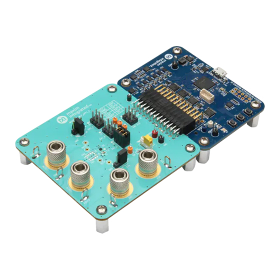
Evaluates: MAX98361 (WLP)
General Description
The MAX98361 evaluation system (EV system) is a
fully assembled and tested system that evaluates the
MAX98361A/B/C/D mono Class-D audio amplifiers.
The EV system consist of a MAX98361 Development
Board (DEV board), Maxim's Audio Interface Board III
(AUDINT3), and a USB cable.
It is recommended that the DEV board be evaluated with
the AUDINT3 board, as an EV system. MAX98361A and
MAX98361C support the standard I
MAX98361B and MAX98361D support standard left-
justified mode. All MAX98361 variants support an
8-channel TDM digital audio interface.
The AUDINT3 board provides the USB-to-PCM interface
in addition to the 1.8V V
the DEV board. The MAX98361 DEV board requires one
additional supply input, 2.5V to 5.5V (V
ing using the AUDINT3 board.
board and the AUDINT3 board.
FOUTN
GND
FOUTP
Figure 1. Simplified EV System Block Diagram
©
2022 Analog Devices, Inc. All rights reserved. Trademarks and registered trademarks are the property of their respective owners.
One Analog Way, Wilmington, MA 01887 U.S.A.
2
S interface, and
supply needed to evaluate
DDIO
) when evaluat-
DD
Figure 1
details the DEV
MAX98361 DEVELOPMENT BOARD
J4
GAI N
MAX98361
U1
J5
VDD
GND
VIN
|
Click
here
to ask an associate for production status of specific part numbers.
MAX98361 Evaluation System
Features
● 2.5V to 5.5V Single-Supply Operation
2
● I
S, Left-Justified, or TDM Input
● Five Selectable Gains (-3dB, 3dB, 6dB, 9dB, and
12dB)
● Audio Channel Select (Left, Right, and Mono Mix)
● Filterless Operation
● Low EMI
● Complete Hardware System with Easy Setup, No
Tools or Special Software Required
EV System Contents
● MAX98361 Development Board
● Audio Interface Board III
● Micro-USB Cable
Ordering Information
J6
J3
J7
BCLK
LRCLK
DIN
J1
J8
EN
SW1
VDDIO
ON
OFF
GND
Tel: 781.329.4700
|
appears at end of data sheet.
AUDIO INTERFACE BOARD 3
J1
USB
INTERFACE
D1
S1
S2
© 2022 Analog Devices, Inc. All rights reserved.
J2
S3
319-100890; Rev 0; 2/22
Advertisement

Related Manuals for Analog Devices MAX98361


Summary of Contents for Analog Devices MAX98361
- Page 1 Figure 1. Simplified EV System Block Diagram 319-100890; Rev 0; 2/22 © 2022 Analog Devices, Inc. All rights reserved. Trademarks and registered trademarks are the property of their respective owners. One Analog Way, Wilmington, MA 01887 U.S.A. Tel: 781.329.4700 © 2022 Analog Devices, Inc. All rights reserved.
-
Page 2: Required Equipment
AUDINT3 Board Setup: puts PCM data to the DIN pin on the DEV board. 1) Connect the MAX98361 DEV board (2 row J1 4) Adjust the audio source volume to a low level. connector) to the AUDINT3 board (3 row J1 5) Enable the audio source and verify that audio is connector). - Page 3 LDO regulator independently powers V on the DEV DDIO The MAX98361 EV system is designed to allow for a thor- board. This power is routed to the DEV board through the ough evaluation of the MAX98361 digital input Class-D J1 connector. See the section.
- Page 4 DAI Configuration A. DAI1 BCLK Channel Selection (TDM Mode) DAI2 LRCLK In TDM mode, the MAX98361 has a fixed gain of 12dB DAI0 and the GAIN_SLOT pin becomes repurposed for TDM channel selection. The MAX98361 accepts 8-channel DAI2 BCLK...
- Page 5 Figure 4 for an illustration radiation. Although it is best to choose filter components of how the MAX98361 DAI interface is routed through the based on EMI test results, the combination of 100pF DAI headers from the AUDINT3 connector. capacitors (C3, C4) and ferrite beads (FB1, FB2) generally work well.
-
Page 6: Ordering Information
MAX98361 Evaluation System Evaluates: MAX98361 (WLP) Audio Interface Board III The MAX98361 DEV board connects to the AUDINT3 board through connector J1. The physical connections Maxim’s Audio Interface board III (AUDINT3 board) facilitates made between the DEV board and AUDINT3 board are... - Page 7 MAX98361 Evaluation System Evaluates: MAX98361 (WLP) MAX98361 EV System DEV Board Bill of Materials ITEM REF_DES DNI/DNP MFG PART # MANUFACTURER VALUE DESCRIPTION COMMENTS TEST POINT; PIN DIA=0.1IN; TOTAL LENGTH=0.3IN; BCLK, DIN, 5003 KEYSTONE BOARD HOLE=0.04IN; ORANGE; PHOSPHOR EN, LRCLK BRONZE WIRE SILVER PLATE FINISH;...
- Page 8 MAX98361 Evaluation System Evaluates: MAX98361 (WLP) MAX98361 EV System PCB Schematic Analog Devices │ 8 www.analog.com...
- Page 9 MAX98361 Evaluation System Evaluates: MAX98361 (WLP) MAX98361 EV System PCB Layout Diagrams 1” MAX98361 EV System—Top Silkscreen MAX98361 EV System—Inner 1 MAX98361 EV System—Top MAX98361 EV System—Inner 2 Analog Devices │ 9 www.analog.com...
- Page 10 MAX98361 Evaluation System Evaluates: MAX98361 (WLP) MAX98361 EV System PCB Layout Diagrams (continued) MAX98361 EV System—Bottom MAX98361 EV System—Bottom Silkscreen Analog Devices │ 10 www.analog.com...
-
Page 11: Revision History
Information furnished by Analog Devices is believed to be accurate and reliable. However, no responsibility is assumed by Analog Devices for its use, nor for any infringements of patents or other rights of third parties that may result from its use.Specifications subject to change without notice. No license is granted by implication or otherwise under any patent or patent rights of Analog Devices.
Need help?
Do you have a question about the MAX98361 and is the answer not in the manual?
Questions and answers