Advertisement
DESCRIPTION
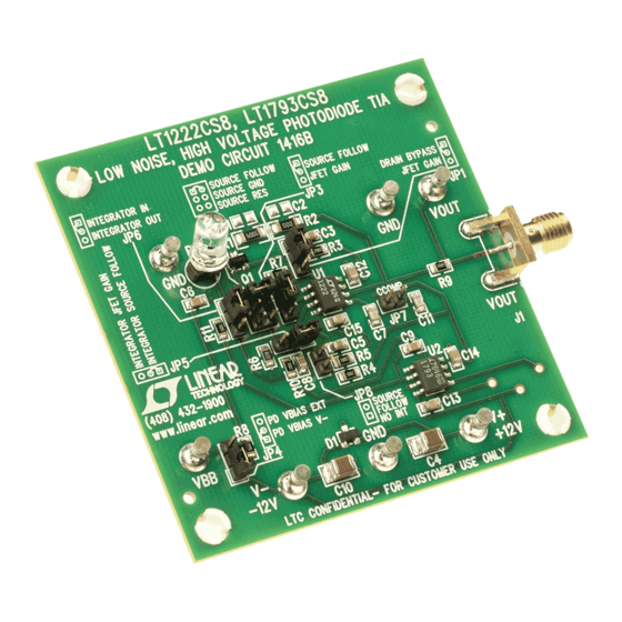
Demonstration circuit 1416 is a low noise transimpedance
amplifier. It utilizes the low voltage noise
and the low current noise
discrete NXP JFET BF862
to take advantage of each component's particular opti-
PERFORMANCE SUMMARY
SYMBOL
PARAMETER
V
Supply Voltage
S
A
TIA Gain
Z
V
Input Offset Voltage
OS
dV
/dT
Input Offset Voltage Drift
OS
I
Input Bias Current
BIAS
en
Input Voltage Noise Density
en
Input Voltage Noise Density
C
Input Capacitance
IN
GBW
Gain Bandwidth Product
GBW
Gain Bandwidth Product
GBW
Gain Bandwidth Product
BW
–3dB Bandwidth
V
Output Voltage Swing
OUT
V
Output Voltage Swing
OUT
V
Output Voltage Swing
OUT
V
Output Voltage Swing
OUT
I
Supply Current
CC
I
Input Bias Current
BIAS
PSRR
Power Supply Rejection Ratio
Note 1) BF862 has been obsoleted as of 2017. On-Semi 2SK932-22 has been substituted, with practically identical performance.
Arrow.com.
Downloaded from
LT
1222
op amp,
®
LT1793
op amp, along with the
1
or equivalent, allowing the user
Specifications are at T
CONDITIONS
LT1793 (V
LT1793 (dV
LT1793 + BF862
f = 100kHz, JFET In Gain Configuration
f = 100kHz, Source Follower Configuration
f = 10kHz, Source Follower Configuration
JP In (C
JP Out (C
JP Out, C7 Removed (C
With SFH213, 1MΩ Gain, JP7 Out
Cathode Input, Integrator In
Cathode Input, Integrator Out
Anode Input, Integrator In
Anode Input, Integrator Out
V
= ±12V
S
LT1793 + BF862
±5V to ±15V, Integrator In
DEMO MANUAL DC1416
LT1222 and LT1793
Transimpedance Amplifier
mization. These components are arranged with jumpers
allowing various composite configurations. A socketed
photodiode, OSRAM SFH213, is also provided.
Design files for this circuit board are available at
http://www.linear.com/demo/DC1416
All registered trademarks and trademarks are the property of their respective owners.
= 25°C, V
= ±12V
A
S
+ I
• 10M)
OS
BIAS
/dT +dI
/dT • 10M)
OS
BIAS
1
= 49pF)
COMP
= 10pF)
COMP
= 0pF)
COMP
1
Low Noise
TYP
UNITS
±12
V
1M
Ω
300
µV
10
µV/C
6
pA
1
nV/√Hz
3
nV/√Hz
2
pF
70
MHz
190
MHz
500
MHz
2
MHz
0 to 10
V
–0.4 to –10
V
0 to –10
V
–0.4 to –10
V
17
mA
6
pA
95
dB
dc1416fa
1
Advertisement
Table of Contents

Related Manuals for Analog Devices LT1222


Summary of Contents for Analog Devices LT1222
- Page 1 DEMO MANUAL DC1416 LT1222 and LT1793 Low Noise Transimpedance Amplifier DESCRIPTION Demonstration circuit 1416 is a low noise transimpedance mization. These components are arranged with jumpers amplifier. It utilizes the low voltage noise 1222 op amp, allowing various composite configurations. A socketed ®...
- Page 2 DEMO MANUAL DC1416 OPERATING PRINCIPLES Composite amplifiers using single JFET inputs can be accuracy, overriding the high 400mV or so V of the classified into two groups: common drain (or “source JFET. The standard jumper configuration is “Integrator follower”) and common source (or “JFET in gain”). The In”, so the TIA will be DC accurate to within the V of the standard jumper configuration of this board, as shipped...
- Page 3 JFET Drain 1, 2 1, 2 2, 3 2, 3 JFET Source 1, 2 1, 2 5, 6 3, 4 LT1222 –Input 1, 2 1, 2 2, 3 2, 3 Photodiode Bias 1, 2 1, 2 1, 2 1, 2...
- Page 4 DEMO MANUAL DC1416 +12V +12V 2.49k BF862 – –12V LT1222 LT1222 3.01k BF862 – DC1416 F02 –12V –12V SOURCE FOLLOWER JFET IN GAIN Figure 2. The Two Basic Types of JFET Configuration. The Left Shows the JFET as a Source Follower, Simply Buffering the Feedback Resistor to the Op Amp’s Inverting Input.
- Page 5 Devices for its use, nor for any infringements of patents or other rights of third parties that may result from its use. Specifications subject to change without notice. No license is granted by implication or otherwise under any patent or patent rights of Analog Devices.
- Page 6 Board until you have read and agreed to the Agreement. Your use of the Evaluation Board shall signify your acceptance of the Agreement. This Agreement is made by and between you (“Customer”) and Analog Devices, Inc. (“ADI”), with its principal place of business at One Technology Way, Norwood, MA 02062, USA. Subject to the terms and conditions of the Agreement, ADI hereby grants to Customer a free, limited, personal, temporary, non-exclusive, non-sublicensable, non-transferable license to use the Evaluation Board FOR EVALUATION PURPOSES ONLY.
Need help?
Do you have a question about the LT1222 and is the answer not in the manual?
Questions and answers