Table of Contents
Advertisement
Quick Links
To our customers,
st
On April 1
, 2010, NEC Electronics Corporation merged with Renesas Technology
Corporation, and Renesas Electronics Corporation took over all the business of both
companies. Therefore, although the old company name remains in this document, it is a valid
Renesas Electronics document. We appreciate your understanding.
Issued by: Renesas Electronics Corporation (http://www.renesas.com)
Send any inquiries to http://www.renesas.com/inquiry.
Old Company Name in Catalogs and Other Documents
Renesas Electronics website:
http://www.renesas.com
st
April 1
, 2010
Renesas Electronics Corporation
Advertisement
Table of Contents

Related Manuals for Renesas Emulation Pod M30620T2-RPD-E


Summary of Contents for Renesas Emulation Pod M30620T2-RPD-E
- Page 1 On April 1 , 2010, NEC Electronics Corporation merged with Renesas Technology Corporation, and Renesas Electronics Corporation took over all the business of both companies. Therefore, although the old company name remains in this document, it is a valid Renesas Electronics document. We appreciate your understanding.
- Page 2 Renesas Electronics. Renesas Electronics shall not be in any way liable for any damages or losses incurred by you or third parties arising from the use of any Renesas Electronics product for an application categorized as “Specific”...
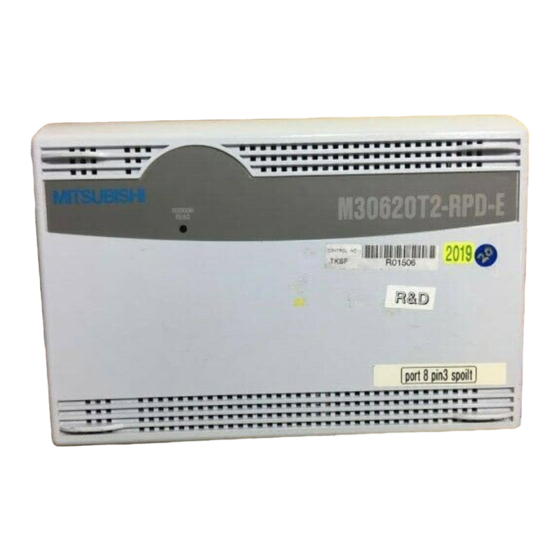
- Page 3 M30620T2-RPD-E User’s Manual Emulation Pod for M16C/62,62A Group MCUs Rev.1.00 2003.07...
- Page 4 • These materials are intended as a reference to assist our customers in the selection of the Renesas Technology product best suited to the customer's application; they do not convey any license under any intellectual property rights, or any other rights, belonging to Renesas Technology Corporation, Renesas Solutions Corporation or a third party.
-
Page 5: Precautions For Safety
Preface The M30620T2-RPD-E is an emulation pod for the M16C/62 and M16C/62A Groups of 16-bit microcomputers. It's used with a PC4701 emulator. This user's manual mainly describes functions of the M30620T2-RPD-E emulation pod and how to operate it. For details on the following products, which are used with M30620T2-RPD-E, refer to each product's user's manual. -
Page 6: Table Of Contents
Contents Chapter 1. Precautions for Safety ... 7 1.1 Safety Symbols and Meanings ... 8 Chapter 2. Preparation ... 17 2.1 Terminology ... 18 2.2 Package Components ... 19 2.3 Other Tool Products Required for Development ... 19 2.4 Name of Each Part ... 20 2.5 When Using the Emulator for the First Time ... - Page 7 (2) Separate Bus, With Wait, Accessing External Memory Area ... 47 (3) Multiplex Bus, With Wait, Accessing External Memory Area ... 49 (4) Timing Requirements ... 51 5.3 Operation Timing of Memory Expansion and Microprocessor Modes (3 V) ... 53 (1) Separate Bus, No-wait ...
- Page 8 MEMO ( 6 / 78 )
-
Page 9: Chapter 1. Precautions For Safety
Note on Software Reset ... 13 Note on Protect Resistor (PRC2) ... 13 Note on Pullup Control Resistor ... 13 Note on Differences between Actual MCU and Emulator ... 14 Note on Switch Settings According to Operation Voltage ... 16 ( 7 / 78 ) -
Page 10: Safety Symbols And Meanings
Chapter 1. Precautions for Safety In both the user's manual and on the product itself, several icons are used to insure proper handling of this product and also to prevent injuries to you or other persons, or damage to your properties. This chapter describes the precautions which should be taken in order to use this product safely and properly. -
Page 11: Warning For Installation
• If the emulator malfunctions because of interference like external noise, do the following to remedy the trouble. (1) Press the RESET switch on the emulator front panel. (2) If normal operation is not restored after step (1), shut OFF power to the emulator once and then reactivate it. -
Page 12: Notes On Downloading Firmware
Notes on Downloading Firmware: • Before using this product for the first time, it is necessary to download the dedicated firmware (control software for the emulation pod built into the PC4701). Please note that, to do this, it is necessary to start up the PC4701 in the maintenance mode. For firmware download procedures, see "4.2 Downloading Firmware"... -
Page 13: Note On Dma Transfer
For this malfunction, when the reading out to the 0 address is generated excluding the interrupt, the yellow LED lights up to alarm. When this LED lights, there is a possibility of wrong access, therefore check the program. This LED is turned off by the RESET switch of the emulator main unit. -
Page 14: Notes On Map References And Settings
Notes on MAP References and Settings: • For details on referencing and setting MAP information, see User's Manual of the emulator debugger M3T-PD30. • Be sure to set the SFR area to EXTERNAL (an external section). • When setting 0FFFC This product uses the 4 byte area 0FFFC cannot be read or written to, reset cannot be properly effected. -
Page 15: Note On Nmi* Input
Note on NMI* Input: • NMI* input from the target system is accepted only while a user program is being executed (only while the RUN status LED on the PC4701's front panel is lit). Note on HOLD* Input: • Be sure to input "L" to the HOLD* pin of the target system during the user program executing. Inputting "L"... -
Page 16: Note On Differences Between Actual Mcu And Emulator
Note on Differences between Actual MCU and Emulator: • Operations of the emulator differs from those of mask MCUs as listed below. (1) Reset condition Set the time for starting up (0.2 Vcc to 0.8 Vcc) 1 µs or less. (2) Data values of ROM area at power-on (3) Internal memories (RAM and ROM) capacities etc. - Page 17 IMPORTANT (7) Output of the actual MCU and this product Table 1.1 Differences of outputs between actual MCU and this product (when executing program) Access area Signal Actual MCU Address BHE* Data (floating during read operating) SFR area (Low at write cycle, (MAP = EXT) Low at read cycle) Does not output...
-
Page 18: Note On Switch Settings According To Operation Voltage
Note on Switch Settings According to Operation Voltage: • With this product, you need to change the switch setting according to the operation voltage. Change the setting as described below. For details, see "3.2 Setting Switches and Pullup Resistor" (page 25). -
Page 19: Chapter 2. Preparation
This chapter describes the package components, the system configuration and the preparation for using this product for the first time. 2.1 Terminology ... 18 2.2 Package Components... 19 2.3 Other Tool Products Required for Development... 19 2.4 Name of Each Part ... 20 (1) System Configuration ... -
Page 20: Terminology
Chapter 2. Preparation 2.1 Terminology Some specific words used in this user's manual are defined as follows: Emulator system This means an emulator system built around the PC4701 emulator. The PC4701 emulator system is configured with an emulator main unit, emulation pod, host machine and emulator debugger. Emulator main unit (Hereafter PC4701) This means a generic name for PC4701M, PC4701HS and PC4701L emulators for 8 and 16-bit MCUs. -
Page 21: Package Components
2.2 Package Components The M30620T2-RPD-E package consists of the following items. When unpacking, check to see if your M30620T2-RPD-E contains all of these items. M30620T2-RPD-E emulation pod main unit FLX120-RPD flexible cable for connecting PC4701 FLX100 flexible cable for connecting pitch converter board (pre-installed in emulation pod) FLX-100LCC pitch converter board for connecting target system OSC-3 (16 MHz) oscillator circuit board (pre-installed in emulation pod) OSC-2 oscillator circuit board... -
Page 22: Name Of Each Part
2.4 Name of Each Part (1) System Configuration Figure 2.1 System configuration (1) to (4) in Figure 2.1 are included with this product package. (1) Emulation pod (M30620T2-RPD-E) This emulation pod contains an evaluation MCU, emulation memory and circuit to feature the debugging function. -
Page 23: Inside Of Emulation Pod
(2) Inside of Emulation Pod Figure 2.2 Internal view of emulation pod (1) MCU-dependent board Board which groups parts (pins and added functions) which vary according to MCU model. (2) Base board Board for the M16C/60 and M16C/20 Series MCUs which controls the interface with the PC4701 and the evaluation MCU. -
Page 24: When Using The Emulator For The First Time
For more information, see each user's manual of the emulator debugger and the PC4701. Within 2 seconds of turning the power ON, press the RESET switch of the PC4701 and check the maintenance mode is accessed. Download the firmware using the emulator debugger. -
Page 25: Chapter 3. Setting Up
This chapter describes switch settings required for using this product and how to connect this product to the PC4701 and the target system. 3.1 Removing the Upper Cover ... 24 3.2 Setting Switches and Pullup Resistor ... 25 3.3 Selecting Clock Supply ... 29 (1) Using the Oscillator Circuit on Target System ... -
Page 26: Removing The Upper Cover
Chapter 3. Setting Up To use this emulation pod with your target system, it is necessary to set as follows. Set the following after removing the upper cover. • Change the oscillation frequency. • Set the X • Set the switches for the operating voltage of the target system. •... -
Page 27: Setting Switches And Pullup Resistor
Figure 3.2 shows the positions of switches and a position for installing a pullup resistor. Tables 3.1, 3.2 list how to set each switch and Figure 3.3 shows how to install a pullup resistor. Figure 3.2 Positions of switches and their factory-settings... - Page 28 Table 3.1 Switch settings of M30620T2-RPD-E (part 1) Signal Switch (Factory-setting) (Factory-setting) BYTE (Factory-setting) Setting OPEN Pulls down the CNV at 33 kΩ. CNVSS OPEN Does not pull down/up the CNV CNVSS Pulls up the CNV OPEN at 33 kΩ.
- Page 29 Table 3.2 Switch settings of M30620T2-RPD-E (part 2) Signal Switch (Factory-setting) COUT (Factory-setting) (Factory-setting) Setting XCOUT OPEN Connects the P8 system. (Uses P8 P86/XCOUT XCOUT Does not connect the P8 OPEN pin as X COUT P86/XCOUT XCOUT Connects the P8 OPEN system.
- Page 30 It is not possible to control the pullup by the pullup control resistor of ports P0 to P5 (possible to read and write by the pullup control resistor). However, as this product has a socket for installing the pullup resistor, it is possible to pull up by mounting the resistor array included with this product.
-
Page 31: Selecting Clock Supply
3.3 Selecting Clock Supply There are two ways to supply a clock to the MCU, using the oscillator circuit of the emulation pod or using the oscillator circuit on the target system. Table 3.3 lists the factory-settings of each clock supply. -
Page 32: Using The Oscillator Circuit On Target System
(1) Using the Oscillator Circuit on Target System When turning on the power supply, the internal clock of emulation pod is selected to supply the clock to the MCU. To use the external clock on the target system, change the clock by the Init dialog when starting up the emulator debugger or the CLK command on the script window. -
Page 33: Changing The Internal Oscillator Circuit Of Emulation Pod
(2) Changing the Internal Oscillator Circuit of Emulation Pod An oscillator circuit board for 16 MHz is mounted on this product. To use the emulation pod at a frequency other than 16 MHz, build the desired oscillator circuit on the included OSC-2 oscillator circuit board (bare board) and replace the board installed in the emulation pod when shipped from the factory. -
Page 34: Replacing The Oscillator Circuit Boards
(3) Replacing the Oscillator Circuit Boards Figure 3.8 shows how to replace the oscillator circuit boards. For the position of the oscillator circuit board, see Figure 2.2. Figure 3.8 Replacing the oscillator circuit boards (1) Unscrew the screw connecting the oscillator circuit board. (2) Lift off the oscillator circuit board. -
Page 35: Connecting The Pc4701 And Emulation Pod
3.4 Connecting the PC4701 and Emulation Pod To connect the emulation pod to the PC4701, use the FLX120-RPD 120-pin flexible cable included with this product package. Connect the PC4701 side connector of FLX120-RPD to the cable connector of the PC4701, then secure with screws the FLX120-RPD. (1) Connecting the Cable to the PC4701 Figure 3.9 shows how to connect the PC4701 and FLX120-RPD Figure 3.9 Connecting PC4701 and FLX120-RPD... -
Page 36: Connecting The Cable To The Emulation Pod
(2) Connecting the Cable to the Emulation Pod Figure 3.10 shows how to connect the FLX120-RPD and the emulation pod. Figure 3.10 Connecting FLX120-RPD and emulation pod Note on Connecting the Cable: • Always shut OFF power before connecting the cable. The power ON state could destroy internal circuits. -
Page 37: Connecting The Target System
3.5 Connecting the Target System There are eight ways available to connect the emulation pod to target systems as shown in Figure 3.11. Figure 3.11 Connecting emulation pod and target systems Notes on Connecting Target Systems: CAUTION • Take care not to attach the converter board in a wrong direction. It may cause a fatal damage to the emulation pod. - Page 38 MEMO ( 36 / 78 )
-
Page 39: Chapter 4. Usage
This chapter describes from turning on the power of this product to starting up the emulator debugger. 4.1 Turning On the Power ... 38 (1) Checking the Connection of the Emulator System ... 38 (2) Turning On the Power... 38 (3) LED Display When PC4701 Starts Up Normally ... -
Page 40: Turning On The Power
Chapter 4. Usage 4.1 Turning On the Power (1) Checking the Connection of the Emulator System Before turning the power ON, check the connection of the PC4701, emulation pod, converter board and target system. (2) Turning On the Power Power ON/OFF the target system and the PC4701 as simultaneously as possible. Notes on Power Supply: CAUTION •... -
Page 41: Led Display When Pc4701 Starts Up Normally
(3) LED Display When PC4701 Starts Up Normally After the emulator starts up, check the status of the LEDs on the front panel to see whether emulation pod operation is enabled or not. Figure 4.1 shows front panel LED lighting status when the emulator is turned ON. -
Page 42: Downloading Firmware
Download the firmware in the maintenance mode as explained here following. The target system must not be connected when downloading the firmware. (1) Within 2 seconds of activating power to the emulator, press the RESET switch on the emulator front panel. This will switch the emulator to the maintenance mode. -
Page 43: Self-Check
(1) Set the switches in the emulation pod same as the factory setting (see Figure 4.3). (2) When the target system is connected, disconnect the target system. (3) Within 2 seconds of activating power to the emulator, press the RESET switch on the emulator front panel to switch the emulator to the maintenance mode. - Page 44 Figure 4.4 Self-check procedure ( 42 / 78 )
-
Page 45: Chapter 5. Specifications
Chapter 5. Specifications This chapter describes specifications of this product. 5.1 Specifications ... 44 5.2 Operation Timing in Memory Expansion and Microprocessor Modes (5 V) ... 45 (1) Separate Bus, No-wait ... 45 (2) Separate Bus, With Wait, Accessing External Memory Area ... 47 (3) Multiplex Bus, With Wait, Accessing External Memory Area ... -
Page 46: Specifications
Chapter 5. Specifications 5.1 Specifications Table 5.1 lists the specifications of M30620T2-RPD-E. Table 5.1 Specifications of M30620T2-RPD-E Emulators Applicable MCUs Evaluation MCU Usable modes Emulation memory Maximum operating frequency Clock supply Operating voltage Operating temperature Storage temperature Power supply to emulation pod Connection to target system Overseas standards PC4701M, PC4701HS or PC4701L... -
Page 47: Operation Timing In Memory Expansion And Microprocessor Modes (5 V)
5.2 Operation Timing in Memory Expansion and Microprocessor Modes (5 V) (1) Separate Bus, No-Wait Table 5.2 and Figure 5.1 show the bus timing in the memory expansion mode and the microprocessor mode (separate bus, no-wait). Table 5.2 Memory expansion mode and microprocessor mode (separate bus, no-wait) Symbol Td (BCLK-AD) Th (BCLK-AD) - Page 48 Memory expansion mode and microprocessor mode (no-wait) Read timing BCLK Write timing BCLK WR, WRL, Figure 5.1 Memory expansion mode and microprocessor mode (no-wait) Conditions: • V = 5 V • Input timing voltage: V • Output timing voltage: V ( 46 / 78 ) = 5 V = 0.8 V, V...
-
Page 49: Separate Bus, With Wait, Accessing External Memory Area
(2) Separate Bus, With Wait, Accessing External Memory Area Table 5.3 and Figure 5.2 show the bus timing in the memory expansion mode and the microprocessor mode (with wait, accessing external memory area). Table 5.3 Memory expansion mode and microprocessor mode (with wait, external memory area) Symbol Td (BCLK-AD) Address output delay time... - Page 50 Memory expansion mode and microprocessor mode (with wait, accessing external memory area) Read timing BCLK Write timing BCLK WR, WRL, Figure 5.2 Memory expansion mode and microprocessor mode (with wait) Conditions: • V =5 V • Input timing voltage: V •...
-
Page 51: Multiplex Bus, With Wait, Accessing External Memory Area
(3) Multiplex Bus, With Wait, Accessing External Memory Area Table 5.4 and Figure 5.3 show the bus timing in the memory expansion mode and the microprocessor mode (with wait, accessing external memory area and using multiplex bus). Table 5.4 Memory expansion mode and microprocessor mode (with wait, multiplex bus) Symbol Td (BCLK-AD) Address output delay time... - Page 52 Memory expansion mode and microprocessor mode (with wait, accessing external memory area and using multiplex bus) Read timing BCLK Write timing BCLK WR, WRL, Figure 5.3 Memory expansion mode and microprocessor mode (with wait, multiplex bus) Conditions: • V =5 V •...
-
Page 53: Timing Requirements
(4) Timing Requirements Table 5.5, Figures 5.4 and 5.5 show timing requirements in the memory expansion mode and the microprocessor mode. Table 5.5 Timing requirements (V Symbol Tsu (DB-RD) Data input setup time Tsu (RDY-BCLK) RDY* input setup time Tsu (HOLD-BCLK) HOLD* input setup time Th (RD-DB) Data input hold time... - Page 54 Common to "with wait" and "no-wait" (actual MCU) BCLK HOLD input HLDA output P0, P1, P2, P3, P4, to P5 Common to "with wait" and "no-wait" (This product) BCLK HOLD input HLDA output P0, P1, P2, P3, P4, to P5 Note 1.
-
Page 55: Operation Timing Of Memory Expansion And Microprocessor Modes (3 V)
5.3 Operation Timing in Memory Expansion and Microprocessor Modes (3 V) (1) Separate Bus, No-Wait Table 5.6 and Figure 5.6 show the bus timing in the memory expansion mode and the microprocessor mode (separate bus, no-wait). Table 5.6 Memory expansion mode and microprocessor mode (separate bus, no-wait) Symbol Td (BCLK-AD) Th (BCLK-AD) - Page 56 Memory expansion mode and microprocessor mode (no-wait) Read timing BCLK Write timing BCLK WR, WRL, Figure 5.6 Memory expansion mode and microprocessor mode (no-wait) Conditions: • V =3 V • Input timing voltage: V • Output timing voltage: V ( 54 / 78 ) = 3 V = 0.48 V, V = 1.5 V...
-
Page 57: Separate Bus, With Wait, Accessing External Memory Area
(2) Separate Bus, With Wait, Accessing External Memory Area Table 5.7 and Figure 5.7 show the bus timing in the memory expansion mode and the microprocessor mode (with wait, accessing external memory area and using multiplex bus). Table 5.7 Memory expansion mode and microprocessor mode (with wait, external memory area) Symbol Td (BCLK-AD) Address output delay time... - Page 58 Memory expansion mode and microprocessor mode (with wait, accessing external memory area) Read timing BCLK Write timing BCLK WR, WRL, Figure 5.7 Memory expansion mode and microprocessor mode (with wait) Conditions: • V =3 V • Input timing voltage: V •...
-
Page 59: Multiplex Bus, With Wait, Accessing External Memory Area
(3) Multiplex Bus, With Wait, Accessing External Memory Area Table 5.8 and Figure 5.8 show the bus timing in the memory expansion mode and the microprocessor mode (with wait, accessing external memory area and using multiplex bus). Table 5.8 Memory expansion mode and microprocessor mode (with wait, multiplex bus) Symbol Td (BCLK-AD) Address output delay time... - Page 60 Memory expansion mode and microprocessor mode (with wait, accessing external memory area and using multiplex bus) Read timing BCLK Write timing BCLK WR, WRL, Figure 5.8 Memory expansion mode and microprocessor mode (with wait, multiplex bus) Conditions: • V =3 V •...
-
Page 61: Timing Requirements
(4) Timing Requirements Table 5.9, Figures 5.9 and 5.10 show timing requirements in the memory expansion mode and the microprocessor mode. Table 5.9 Timing requirements (V Symbol Tsu (DB-RD) Data input setup time Tsu (RDY-BCLK) RDY* input setup time Tsu (HOLD-BCLK) HOLD* input setup time Th (RD-DB) Data input hold time... - Page 62 Memory expansion mode and microprocessor mode Common to "with wait" and "no-wait" (actual MCU) BCLK HOLD input HLDA output P0, P1, P2, P3, P4, to P5 Common to "with wait" and "no-wait" (this product) BCLK HOLD input HLDA output P0, P1, P2, P3, P4, to P5 Note 1.
-
Page 63: Electrical Characteristics
5.4 Electrical Characteristics Tables 5.10 and 5.11 list IC electrical characteristics of the user interface. Table 5.10 Electrical characteristics of 74HC4066AFT Symbol High level control input voltage Low level control input voltage ON resistance Difference of ON resistances Table 5.11 Electrical characteristics of M60081L-0142FP (P0 Symbol Input voltage Output voltage... -
Page 64: Connection Diagram
5.5 Connection Diagram Figures 5.11 and 5.12 show the connection diagram of M30620T2-RPD-E. This connection diagram mainly shows the interface section, and the circuits which are not connected to the target system such as the emulator's control system are omitted. Figure 5.11 Connection diagram 1 ( 62 / 78 ) - Page 65 Figure 5.12 Connection diagram 2 ( 63 / 78 )
-
Page 66: External Dimensions
5.6 External Dimensions (1) External Dimensions of Emulation Pod Figure 5.13 External dimensions of M30620T2-RPD-E ( 64 / 78 ) -
Page 67: External Dimensions Of Pitch Converter Board (Flx-100Lcc)
(2) External Dimensions of Pitch Converter Board (FLX-100LCC) Figure 5.14 shows the external dimensions of the pitch converter board FLX-100LCC for 100-pin LQFP (100D0). Figure 5.14 External dimensions of pitch converter board (FLX-100LCC) ( 65 / 78 ) - Page 68 MEMO ( 66 / 78 )
-
Page 69: Chapter 6. Troubleshooting
Chapter 6. Troubleshooting This chapter describes how to troubleshoot when this product does not work properly. 6.1 Flowchart to Remedy the Troubles ... 68 6.2 When the Emulator Debugger Does Not Start Up Properly... 69 (1) When the LED Display of PC4701 is Abnormal ... 69 (2) Errors Occur When the Emulator Debugger Starts Up (When the target system is connected) ... -
Page 70: Flowchart To Remedy The Troubles
Chapter 6. Troubleshooting 6.1 Flowchart to Remedy the Troubles Figure 6.1 shows the flowchart to remedy the troubles from when power to the emulator is activated until the emulator debugger starts up. Check this while the target system is disconnected. Turning on the power of PC4701 Program window of emulator debugger displayed Figure 6.1 Flowchart to remedy the troubles... -
Page 71: When The Emulator Debugger Does Not Start Up Properly
6.2 When the Emulator Debugger Does Not Start Up Properly (1) When the LED Display of PC4701 is Abnormal Table 6.1 LED's abnormal display and its checkpoints Error LEDs do not light up. All LEDs remain lit. The "POWER" LED of "STATUS OF TARGET"... -
Page 72: (When The Target System Is Connected)
(2) Errors Occur When the Emulator Debugger Starts Up (When the target system is connected) Table 6.2 Checkpoints of errors when starting up the emulator debugger (target is connected) Error Communication error occurred Data was not sent to the target Target system cannot be properly built PD30 version is not the same version as the firmware in the target... -
Page 73: (When The Target System Is Not Connected)
(1) Does Not Operate with Operating Frequencies (3.6 V to 5.5 V) Properly With this product, you need to change the switch setting according to the operation voltage. Change the setting as described below. For details, see "3.2 Setting Switches and Pullup Resistor" (page 25). -
Page 74: Data Values Of Rom Area At Power-On Are Different
(4) Data Values of ROM Area at Power-on Are Different For this product, 04h is written into the ROM area at power-on. Therefore, the data values are different from those of an actual MCU. (5) HOLD* control When inputting "Low" to the HOLD* pin to run into the HOLD state, P0 state delaying by 2.5 cycles than the actual MCU (see Table 5.5, Figure 5.5, Table 5.9 and Figure 5.10). -
Page 75: Chapter 7. Maintenance And Guarantee
Chapter 7. Maintenance and Guarantee This chapter describes how to maintenance, repair provisions and how to request for repair. 7.1 Maintenance ... 74 7.2 Guarantee ... 74 7.3 Repair Provisions... 74 7.4 How to Request for Repair ... 75 ( 73 / 78 ) -
Page 76: Maintenance
Chapter 7. Maintenance and Guarantee 7.1 Maintenance If dust or dirt collects on any equipment of your emulation system, wipe it off with a dry soft cloth. Do not use thinner or other solvents because these chemicals can cause the equipment's surface coating to separate. -
Page 77: How To Request For Repair
After checking the contents of fault, the distributor should please send the faulty product along with the Repair Request Sheet to Renesas Solutions Corp. When the faulty product is repaired, it will be returned to the customer at the earliest convenience. - Page 78 MEMO ( 76 / 78 )
- Page 79 M30620T2-RPD-E User's Manual Rev. 1.00 July 1, 2003 REJ10J0196-0100Z COPYRIGHT ©2003 RENESAS TECHNOLOGY CORPORATION AND RENESAS SOLUTIONS CORPORATION ALL RIGHTS RESERVED...
- Page 80 M30620T2-RPD-E User’s Manual 1753, Shimonumabe, Nakahara-ku, Kawasaki-shi, Kanagawa 211-8668 Japan REJ10J0196-0100Z...
Need help?
Do you have a question about the Emulation Pod M30620T2-RPD-E and is the answer not in the manual?
Questions and answers