JVC FS-G5 Service Manual
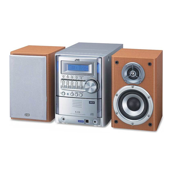
Compact component system
Hide thumbs
Also See for FS-G5:
- Instructions manual (49 pages) ,
- Instructions manual (56 pages) ,
- Instructions manual (30 pages)
Advertisement
Quick Links
SERVICE MANUAL
COMPACT COMPONENT SYSTEM
5
2005
MB353
Lead free solder used in the board (material : Sn-Ag-Cu, melting point : 219 Centigrade)
1
PRECAUTION. . . . . . . . . . . . . . . . . . . . . . . . . . . . . . . . . . . . . . . . . . . . . . . . . . . . . . . . . . . . . . . . . . . . . . . . . 1-3
2
SPECIFIC SERVICE INSTRUCTIONS . . . . . . . . . . . . . . . . . . . . . . . . . . . . . . . . . . . . . . . . . . . . . . . . . . . . . . 1-6
3
DISASSEMBLY . . . . . . . . . . . . . . . . . . . . . . . . . . . . . . . . . . . . . . . . . . . . . . . . . . . . . . . . . . . . . . . . . . . . . . . 1-7
4
ADJUSTMENT . . . . . . . . . . . . . . . . . . . . . . . . . . . . . . . . . . . . . . . . . . . . . . . . . . . . . . . . . . . . . . . . . . . . . . . 1-20
5
TROUBLESHOOTING . . . . . . . . . . . . . . . . . . . . . . . . . . . . . . . . . . . . . . . . . . . . . . . . . . . . . . . . . . . . . . . . . 1-21
FS-G5
TABLE OF CONTENTS
COPYRIGHT © 2005 Victor Company of Japan, Limited
Area suffix
J ---------------------------- U.S.A.
C ------------------------- Canada
No.MB353
2005/5
Advertisement

Related Manuals for JVC FS-G5


Summary of Contents for JVC FS-G5
-
Page 1: Table Of Contents
SERVICE MANUAL COMPACT COMPONENT SYSTEM MB353 2005 FS-G5 Area suffix J ---------------------------- U.S.A. C ------------------------- Canada Lead free solder used in the board (material : Sn-Ag-Cu, melting point : 219 Centigrade) TABLE OF CONTENTS PRECAUTION............... . . 1-3 SPECIFIC SERVICE INSTRUCTIONS . - Page 2 SPECIFICATION Amplifier section Output Power 90 W per channel, min. RMS, driven into 6Ω at 1 kHz with no more than 10% total harmonic distortion. Speakers Impedance 6Ω - 16Ω Audio Input AUX:400 mV/50 kΩ USB:USB Ver. 1.1 Tuner section FM tuning range 87.5 MHz - 108.0 MHz AM tuning range...
-
Page 3: Precaution
SECTION 1 PRECAUTION Safety Precautions (1) This design of this product contains special hardware and voltmeter. many circuits and components specially for safety purpos- Move the resistor connection to each exposed metal es. For continued protection, no changes should be made part, particularly any exposed metal part having a return to the original design unless authorized in writing by the path to the chassis, and measure the AC voltage across... - Page 4 Preventing static electricity Electrostatic discharge (ESD), which occurs when static electricity stored in the body, fabric, etc. is discharged, can destroy the laser diode in the traverse unit (optical pickup). Take care to prevent this when performing repairs. 1.5.1 Grounding to prevent damage by static electricity Static electricity in the work area can destroy the optical pickup (laser diode) in devices such as laser products.
- Page 5 Importance administering point on the safety Caution: For continued protection against risk of fire, replace only with same type 2.5 A/250 V for F901. This symbol specifies the type of fast operating fuse. Precaution: Pour la protection continue contre les risques d'incendie, remplacer uniquement par le meme type: fusible 2.5 A/250 V pour le F901.
-
Page 6: Specific Service Instructions
SECTION 2 SPECIFIC SERVICE INSTRUCTIONS This service manual does not describe SPECIFIC SERVICE INSTRUCTIONS. 1-6 (No.MB353) -
Page 7: Disassembly
SECTION 3 DISASSEMBLY Main body 3.1.1 Removing the side panel (R)/ (L) (See Fig.1 to 3) (1) Remove the three screws A attaching the side panel (R) on the back side and remove the screw A and B on the right side. - Page 8 3.1.2 Removing the top panel (See Fig.4 to 7) • Prior to performing the following procedure, remove the side panel (R)/(L). (1) From the back of the body, remove the screw D attaching Top panel the top panel. (2) From each side of the body, remove the screw E attaching the top panel.
- Page 9 3.1.3 Front panel assembly section 3.1.3.1 Removing the front panel assembly (See Fig.8 to 10) • Prior to performing the following procedure, remove the side Main board panel (R)/(L) and the top panel. Front panel assembly CN671 CN402 (1) From top of the body, disconnect the card wire from con- on the main board and disconnect the wire nector CN402...
- Page 10 3.1.3.2 Removing the LCD & function board (See Fig.11) • Prior to performing the following procedure, remove the front panel assembly. Front panel assembly (1) Pull out the volume knob on the front side of front panel as- sembly. (2) Remove the eight screws H attaching the LCD & function board.
- Page 11 3.1.4 Removing the main board (See Fig.13, 14) • Prior to performing the following procedure, remove the side panel (R)/(L) and the top panel. Main board (1) Disconnect the card wire from connector CN401, CN402, CN402 CN661 CN681 CN401 CN661 CN681 on the main board and disconnect the CN671...
- Page 12 3.1.5 Removing the tuner pack (See Fig.15) • Prior to performing the following procedure, remove the side panel (R)/(L) and the top panel. Tuner pack (1) Disconnect the card wire from connector of the tuner pack. Connector (2) From the back of the body, remove the two screws N at- taching the tuner pack.
- Page 13 3.1.7 Removing the fan (See Fig.17) • Prior to performing the following procedure, remove the side panel (R)/(L), the top panel and the transformer board. (1) From the left side of the body, disconnect the wire from connector CN105 on the amplifier board. (2) From the back of the body, remove the four screws Q at- taching the fan.
- Page 14 3.1.8 Removing the amplifier board/ heat sink (See Fig.18, 19) • Prior to performing the following procedure, remove the side panel (R)/(L), the top panel, the main board, the transformer board, the tuner pack and the fan. Amplifier board (1) From top of the body, disconnect the wire from connector CN101 CN204 on the amplifier board.
- Page 15 3.1.9 Removing the power transformer assembly/ power cord (See Fig.20 to 24) • Prior to performing the following procedure, remove the side panel (R)/(L), the top panel, the main board, the transformer Rear panel board, the fan and the amplifier board. Reference: You do not need remove the tuner pack which is attached to the rear panel.
- Page 16 3.1.10 CD changer mechanism assembly section 3.1.10.1 Removing the CD changer mechanism assembly (See Fig.25 to 30) • Prior to performing the following procedure, remove the side panel (R)/(L), the top panel, the main board, the transformer CD changer mechanism assembly board, the fan, the amplifier board and the rear panel.
- Page 17 CD changer mechanism assembly CD changer machanism cover Point Base chassis Point Point Point Bracket Fig.29 CD changer mechanism assembly Bracket Fig.27 CD changer mechanism assembly Bracket Fig.30 Bracket Fig.28 (No.MB353)1-17...
- Page 18 3.1.10.2 Removing the CD changer mechanism board (See Fig.31 to 33) • Prior to performing the following procedure, remove the CD changer mechanism assembly. CD changer mechanism board Caution: Make sure to solder the short-circuit point on the CD pickup board before disconnecting the card wire connected to con- nector CN701...
- Page 19 3.1.10.3 Removing the CD changer mechanism (See Fig.34, 35) • Prior to performing the following procedure, remove the CD changer mechanism assembly and CD changer mechanism CD changer mechanism assembly board. (1) Remove the three screws F' attaching the CD changer mechanism holder.
-
Page 20: Adjustment
SECTION 4 ADJUSTMENT This service manual does not describe ADJUSTMENT. 1-20 (No.MB353) -
Page 21: Troubleshooting
SECTION 5 TROUBLESHOOTING This service manual does not describe TROUBLESHOOTING. (No.MB353)1-21... - Page 22 Victor Company of Japan, Limited AV & MULTIMEDIA COMPANY AUDIO/VIDEO SYSTEMS CATEGORY 10-1,1chome,Ohwatari-machi,Maebashi-city,371-8543,Japan (No.MB353) Printed in Japan...
- Page 23 SCHEMATIC DIAGRAMS COMPACT COMPONENT SYSTEM FS-G5 CD-ROM No.SML200505 Area suffix J ---------------------------- U.S.A. C ------------------------- Canada SP-FSG5 CA-FSG5 SP-FSG5 Lead free solder used in the board (material : Sn-Ag-Cu, melting point : 219 Centigrade) Contents Wiring diagram Block diagram Standard schematic diagrams...
- Page 24 In regard with component parts appearing on the silk-screen printed side (parts side) of the PWB diagrams, the parts that are printed over with black such as the resistor ( ), diode ( ) and ICP ( ) or identified by the " " mark nearby are critical for safety.
- Page 25 < M E M O >...
- Page 26 Wiring diagram BI12P70100V BI1206561V BI1206821Y CN681 CN671 CN402 MAIN PCB CD P CN661 CN501 CN601 CN802 CN872 BI1206851V BI1206841V (Board to Board) (Board to Board) LC01 CN202 CN201 AMPLIFIER PCB LCD & KEY PCB HP PCB USB/AUX PCB CN105 CN204 BI12P402341 (Tra TUNER MODULE...
- Page 27 BI12P60170V CN702 CN871 CD MECH CD PCB BI1206561Y CN802 CN801 CN872 CN873 BI1206841V (Board to Board) 5CD LDADER W/CD MECH PICKUP ard) CN202 CN201 L901 (Power cord) AMPLIFIER PCB PT PCB BI12P60170V MAIN (Transformer wire) TRANSFORMER...
- Page 28 Block diagram PICKUP ASS'Y DIGITAL OUTPUT RF & SERVO DIGITAL SERVO & A B C D AIGNAL PROCESSOR ANALOG OUTPUT SIL9226 S5L9279 LCD D DRAM FOR MP3 DRAM TRA MECHA ASS'Y BR93L56RF K4S161622H TRVP SPOUT TRACKING COIL CD CONTROL MICON MN101C61G FOCUS COIL DRIVER...
- Page 29 LCD DISPLAY TUNER MODULE FM/AM USB IN PCM2704DB KEY CONTROL ST LED AUX IN TUNER-L 47K IMPEDANCE TUNER-R DATA IN CLK1 DATA OUT D-GND RDS CLK RDS DATA VOLTAGE SUPPLY STK433_090 70W X 2 AMP FUNC IC L/R CH BD3881FV SYSTEM MICON VOLUME S3C825A...
- Page 30 Standard schematic diagrams Front & Power supply section...
- Page 31 Parts are safety assurance parts. When replacing those parts make sure to use the specified one.
- Page 32 Main section...
- Page 34 Amp section...
- Page 35 2-10...
- Page 36 CD section 2-11...
- Page 37 2-12...
- Page 38 Printed circuit boards Main board (forward side) Lead free solder used in the board (material : Sn-Ag-Cu, melting point : 219 C 2-13...
- Page 39 -Cu, melting point : 219 Centigrade) 2-14...
- Page 40 Main board (reverse side) Lead free solder used in the board (material : Sn-Ag-Cu, melting point : 219 Centigrad 2-15...
- Page 41 ng point : 219 Centigrade) 2-16...
- Page 42 Amp board (forward side) Lead free solder used in the board (material : Sn-Ag-Cu, melting point : 219 Centi 2-17...
- Page 43 solder used in the board (material : Sn-Ag-Cu, melting point : 219 Centigrade) 2-18...
- Page 44 Amp board (reverse side) Lead free solder used in the board (material : Sn-Ag-Cu, melting point : 219 Centigrade) 2-19...
- Page 45 in the board (material : Sn-Ag-Cu, melting point : 219 Centigrade) 2-20...
- Page 46 CD board (forward side) Lead free solder used in the board (material : Sn-Ag-Cu, melting point : 219 Centigrade) 2-21...
- Page 47 CD board (reverse side) Lead free solder used in the board (material : Sn-Ag-Cu, melting point : 219 Centigrade) 2-22...
- Page 48 Trans board Lead free solder used in the board (material : Sn-Ag-Cu, melting point : 219 Centigrade) 2-23...
- Page 49 < M E M O >...
- Page 50 Victor Company of Japan, Limited AV & MULTIMEDIA COMPANY AUDIO/VIDEO SYSTEMS CATEGORY 10-1,1chome,Ohwatari-machi,Maebashi-city,371-8543,Japan Printed in Japan (No.MB353SCH)
- Page 51 PARTS LIST [ FS-G5 ] * All printed circuit boards and its assemblies are not available as service parts. Area suffix J ----------------------------- U.S.A. C -------------------------- Canada - Contents - 3- 2 Exploded view of general assembly and parts list (Block No.M1) 3- 5 CD mechanism assembly and parts list (Block No.MB)
- Page 52 Exploded view of general assembly and parts list Block No. F901 Power trans. board Front board 14 15 Dhp board Dusb board CD board...
- Page 53 Amp. board Main board 43 44...
- Page 54 General Assembly Block No. [M][1][M][M] Symbol No. Part No. Part Name Description Local BI1080679101V1 FRONT CABINET BIBT000418 TAPPING SCREW (x23) BI1081770201X1 SLIDE BLOCK BI1080690101V1 CD DOOR BI1080770101V1 BOTTOM LENS R BI1080780101V1 BOTTOM LENS L BI202904010101 CD DOOR SPRING BI1080750101V1 TOP LENS R BI1080760101V1 TOP LENS L...
- Page 55 CD mechanism assembly and parts list Block No. The parts without symbol number are not service.
- Page 56 CD mechanism Block No. [M][B][M][M] Symbol No. Part No. Part Name Description Local BIAJ7000601E CHASSIS BIAJ6600601G GEAR COVER BIAJ6600601D GEAR BIAJ6600601B GEAR BIAJ6600601F GEAR BIAJ7000601A SHAFT BISOHAAN PICK UP BIAJ3100601B SPINDLE MOTOR BIAJ3100601A FEED MOTOR BIAJ6000601D SCREW M2XL3(x4) BI3409000174 LEAF SWITCH BIAJ4100601E SUB PCB...
- Page 57 Electrical parts list Main board Symbol No. Part No. Part Name Description Local Block No. [0][1] C509 BICE475500MP015 E CAPACITOR 4.7uF 50V Symbol No. Part No. Part Name Description Local C510 BICE475500MP015 E CAPACITOR 4.7uF 50V C511 BICE475500MP015 E CAPACITOR 4.7uF 50V C609...
- Page 58 Symbol No. Part No. Part Name Description Local Symbol No. Part No. Part Name Description Local R444 BIRC1010085M000 C RESISTOR 100Ω 1/8W R663 BIRC1220105A005 C RESISTOR 1.2KΩ 1/10W R445 BIRC1010085N000 C RESISTOR 100Ω 1/8W R664 BIRC1220105A005 C RESISTOR 1.2KΩ...
- Page 59 Symbol No. Part No. Part Name Description Local Symbol No. Part No. Part Name Description Local D552 1SS355 DIODE BI31SS355A0077 R391 BIRC2020105A005 C RESISTOR 2KΩ 1/10W D553 1SS355 DIODE BI31SS355A0077 R392 BIRC3020105A005 C RESISTOR 3KΩ 1/10W D581 1SS355 DIODE BI31SS355A0077 R393...
- Page 60 Power trans board Symbol No. Part No. Part Name Description Local Block No. [0][3] C718 BICC102500JA041 C CAPACITOR 1000pF 50V Symbol No. Part No. Part Name Description Local C719 BICC104250KA042 C CAPACITOR 0.1uF 25V C720 BICC333250KA042 C CAPACITOR 0.033uF 25V C721 BICC474100KA042...
- Page 61 Symbol No. Part No. Part Name Description Local Symbol No. Part No. Part Name Description Local R705 BIRC3930105A005 C RESISTOR 39KΩ 1/10W R890 BIRC1020085N000 C RESISTOR 1KΩ 1/8W R706 BIRC3930105A005 C RESISTOR 39KΩ 1/10W R891 BIRC1020105A005 C RESISTOR 1KΩ...
- Page 62 Symbol No. Part No. Part Name Description Local Symbol No. Part No. Part Name Description Local Q204 DTA114YK TRANSISTOR BI2DTA114YKA011 C202 BICE476250MP015 E CAPACITOR 47uF 25V Q241 2SA1235F TRANSISTOR BI2SA1235FA012V C203 BICE105500MP015 E CAPACITOR 1uF 50V Q242 2SA1235F TRANSISTOR BI2SA1235FA012V C204...
- Page 63 Symbol No. Part No. Part Name Description Local R279 BIRC2200085A002 C RESISTOR 22Ω 1/8W R280 BIRC2200085A002 C RESISTOR 22Ω 1/8W R281 BIRC2200085A002 C RESISTOR 22Ω 1/8W R282 BIRC2200085A002 C RESISTOR 22Ω 1/8W R283 BIRC1030105A005 C RESISTOR 10KΩ 1/10W R284 BIRC1030105A005 C RESISTOR 10KΩ...
- Page 64 Packing materials and accessories parts list Block No. No additional / supplemental order of WARRANTY CARDs are available. A1A2 A4 A1A2 A3 FS-G5_J FS-G5_C A5 A6 3-14...
- Page 65 Packing and Accessories Block No. [M][3][M][M] Symbol No. Part No. Part Name Description Local BI440001528000W INST BOOK ENG FRE BI440001507001W INST BOOK BI400023260002W SAFTEY CARD BI4000132820020 GRANTIE CARD ------------ WARRANTY CARD BT-51034-2 ------------ BATTERY (x2) BIAN01281V AM LOOP ANT BIAN01022 ANT WIRE FM BI643FSG5050...
Need help?
Do you have a question about the FS-G5 and is the answer not in the manual?
Questions and answers