Table of Contents
Advertisement
Quick Links
Advertisement
Table of Contents

Subscribe to Our Youtube Channel
Related Manuals for Chauvin Arnoux ULYS FLEX MODBUS


Summary of Contents for Chauvin Arnoux ULYS FLEX MODBUS
- Page 1 GB - User’s manual...
- Page 2 First edition, May 2018. REGISTERED TRADEMARKS ULYS FLEX MODBUS is a trademark registered by CA ENERGY. EQUIPMENT END-OF-LIFE The products which we sell do not fall within the scope of Decree No. 2005-829 relating to the construction of electrical and electronic equipment and the disposal of waste arising from this equipment.
- Page 3 M A N U A L U s e & P ro g r a m m i n g M O D B U S Communication Protocol...
- Page 5 M A N U A L U s e & P ro g r a m m i n g...
-
Page 6: Table Of Contents
INDEX • Use&Programming 1. Introduction ........................7 1.1 SAFETY PRECAUTIONS ................................7 2. Graphic symbols ......................8 3. Preliminary verification ....................8 4. General description ......................8 5. Installation ........................9 5.1 ENVIRONMENTAL REQUIREMENTS............................9 5.2 MOUNTING ....................................9 6. Safety measures ......................9 7. Electrical connections ....................10 7.1 CURRENT AND VOLTAGE INPUTS ............................ -
Page 7: Introduction
1. INTRODUCTION You have just purchased an ULYS FLEX MODBUS. Thank you for your choice. To get the best from your device: • Read this user’s manual before installing and using the device. • Follow the precautions for use stated in this document. -
Page 8: Graphic Symbols
2. GRAPHIC SYMBOLS In this manual, some instructions are highlighted with graphic symbols to alert the reader to possible danger. These symbols are: DANGER! This symbol warns of the presence of dangerous voltage (even for short moments) on the indicated points. WARNING! This symbol alerts you to the possibility of a serious incident or damage to the unit if proper precautions are not taken. -
Page 9: Installation
5. INSTALLATION NOTE. The equipment complies with the 89/366/EEC, 73/23/EEC standards and following amendments. However, if not properly installed, it may generate a magnetic field and radio interference. This is why compliance with EMC standards on electromagnetic compatibility is essential. 5.1 ENVIRONMENTAL REQUIREMENTS The environment in which the instrument is installed must satisfy the following features: •... -
Page 10: Electrical Connections
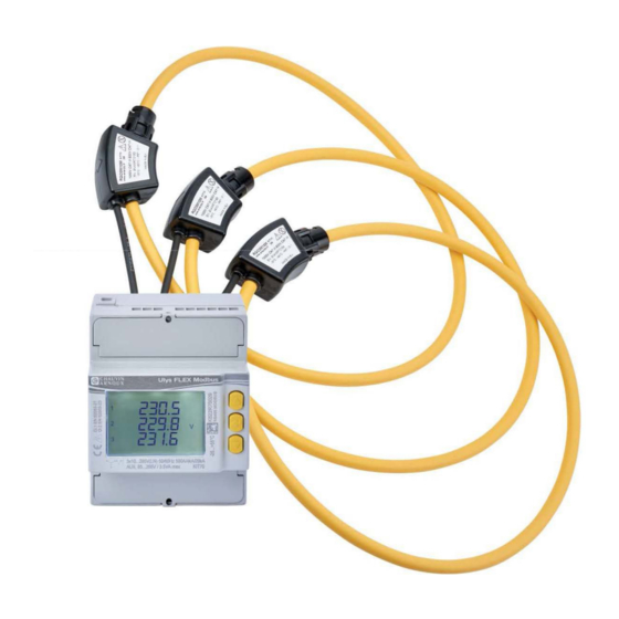
7. ELECTRICAL CONNECTIONS WARNING! The instrument installation and use must be carried out only by qualified staff. Switch off the voltage before device installation. 7.1 CURRENT AND VOLTAGE INPUTS DANGER! This section describes the measurement voltage and current inputs susceptible to dangerous voltage levels. -
Page 11: Power Supply
Wiring diagrams using voltage transformers: 3 phase, 4 wires 3 phase, 3 wires 1 phase Instrument with voltage transformer For wiring mode selection, refer to section 8.14.1. 7.2 POWER SUPPLY DANGER! This section describes the AUX supply input susceptible to dangerous voltage levels. WARNING! Before carrying out connections, check if there is no voltage/current in the conductor wires. -
Page 12: Rs485 Communication Port
7.3 RS485 COMMUNICATION PORT WARNING! Before carrying out connections, check if there is no voltage/current in the conductor wires. DO NOT CONNECT conductors under voltage/current. The RS485 serial communication port allows to manage the instrument in local or remote mode by PC. For a local connection, a converter is needed to adapt the PC USB port to the RS485 network. -
Page 13: Digital Output
7.5 DIGITAL OUTPUT WARNING! Before carrying out connections, check if there is no voltage/current in the conductor wires. DO NOT CONNECT conductors under voltage/current. The instrument is provided with a passive optoisolated digital output for pulse emission or alarm. For digital output setup, refer to section 8.13.1. Digital output Use &... -
Page 14: Use And Configuration
8. USE AND CONFIGURATION At first instrument power on, the following pages will be displayed. Instrument name Firmware release Real time values The page sequence is the same for the further power on times, except for Real time value page. After Firmware release page, it will be displayed: •... - Page 15 SYMBOL MEANING WHERE Clock status Setup page for date and time. User setup, page for date&time Info page for date and time. Info, page for date&time Undefined date and time (no clock setup after power on). Any page except Setup BLINKING Memory/data recording status User setup, page for data...
-
Page 16: Page Structure
8.2 PAGE STRUCTURE Up to 6 page loops are available on the the instrument display. Each loop corresponds to a specific type of data displayed on more pages. Inside each loop it is possible to scroll the available pages. With change the loop 1...6. -
Page 17: Loop 1 - Real Time Values
8.4 LOOP 1 - REAL TIME VALUES In this loop, the real time and the corresponding min/max values are displayed according to the set wiring mode. Scroll the loop pages with button. The following pages refer to the instrument with 3 phase, 4 wire, 3 current insertion. NOTE. -
Page 18: Measurement Overflow
8.5 MEASUREMENT OVERFLOW According to EN 61010-2-030, in case of too high value supplied to the device, the display must inform the user precisely that it is a dangerous overflow (OVF) situation. When an overflow condition occurs, for the relative parameter “----” and symbol are blinking on display. -
Page 19: Real Time Parameter Table
8.7 REAL TIME PARAMETER TABLE The following table shows the parameters available according to the instrument model and the set wiring mode. The column “DISPLAY PAGE” shows the number of the corresponding device page shown in section 8.4. WIRING MODES (=available) DISPLAY MAX () MIN () -
Page 20: Loop 2 - Dmd Values
8.8 LOOP 2 - DMD VALUES In this loop, the demand values (DMD) and the corresponding max values are displayed according to the instrument model and the set wiring mode. The demand values are calculated according to the set DMD calculation mode and integration time (refer to section 8.13.2). -
Page 21: Loop 4 - Energy Counters
8.11 LOOP 4 - ENERGY COUNTERS In this loop, the energy counters are displayed according to the set wiring mode. Scroll the loop pages with button. The following pages refer to the instrument with 3 phase, 4 wire, 3 current insertion. Use &... - Page 22 Use & Programming...
-
Page 23: Energy Counter Table
8.12 ENERGY COUNTER TABLE The following table shows the parameters available according to the instrument model and the set wiring mode. The column “DISPLAY PAGE” shows the number of the corresponding device page shown in section 8.11. In 1 phase insertion, BALANCE values are resulting from the difference between the phase 1 imported energy and the phase 1 exported energy (L1 - L1 WIRING MODES (=available) - Page 24 WIRING MODES (=available) DISPLAY PARAMETER PAGE 3ph, 4w, 3c 3ph, 3w, 3c 3ph, 3w, 2c 1phase +kVAh∑-C • System imported capacitive apparent energy -kVAh∑-C • System exported capacitive apparent energy +kVAh∑-L • System imported inductive apparent energy ...
-
Page 25: Loop 5 - User Setup
8.13 LOOP 5 - USER SETUP In this loop, pages for general instrument setup are displayed according to the instrument model. To access User setup loop, on Setup? page press button for at least 3 s. The first User setup page will be displayed. - Page 26 3. In case of real time or DMD parameter selection, the third row will display hysteresis value. After threshold selection, the hysteresis first digit will start to blink. With button select the digit and confirm with button. Repeat the same procedure for the other digit. Value range: 0...50%. In case of Active power sign parameter selection, the third row will display the delay value.
- Page 27 8.13.2 DMD calculation setup WARNING! If the DMD mode or the integration time is modified, the instrument will reset the DMD & DMD MAX values and restart the DMD period. The following DMD calculation mode is available: • Fixed window (FIX): the DMD value is updated only at the end of the DMD period. The integration time will start to blink.
- Page 28 8.13.4 Energy counter reset By this page, it is possible to reset an energy counter group. According to the displayed symbols, the energy counter group can be identified as follows: • kWh: imported active energies ( +kWh1, +kWh2, +kWh3, +kWh∑ •...
- Page 29 8.13.6 DMD MAX value reset By this page, it is possible to reset DMD MAX values in groups. According to the displayed symbols, the DMD MAX value group can be identified as follows: • Gr 1 (kW): DMD MAX imported active powers ( +P1, +P2, +P3, +P∑...
- Page 30 8.13.8 Data recording setup WARNING! If the recording setup is modified, the recorded data will be deleted and it will not be retrievable. WARNING! If the date&time is lost or modified, the recording is automatically stopped. It is suggested to download the recorded data and set again date&time. Restart the recording by setting the rate, the old recorded data will be deleted.
-
Page 31: Loop 7 - Installation Setup
8.14 LOOP 7 - INSTALLATION SETUP In this loop, pages for the installation setup are displayed according to the instrument model and its wiring mode. To access Installation setup loop, on any page (except for User setup pages) press SET button for at least 3 s. - Page 32 8.14.3 Current full scale (FSA) setup WARNING! If the current full scale (FSA) is modified, the instrument will: • reset all MIN/MAX values, all DMD values, all energy counters • set digital output to the default settings (disabled) • set the default recording setup (disabled) and delete all recorded data WARNING! The current full scale value (FSA) depends on the PT ratio.
- Page 33 8.14.5 Communication speed selection By this page, it is possible to select the communication speed. Selectable values: 300, 600, 1.2k, 2.4k, 4.8k, 9.6k, 19.2k, 38.4k, 57.6k bps. Example: 19.2k=19200 bps To change the value, press button, the corresponding item will start to blink. With button select the communication speed and confirm with ...
-
Page 34: Loop 6 - Info
8.15 LOOP 6 - INFO In this loop, the instrument information is displayed. Scroll the loop pages with button. The following table shows the information available on display. The column “PAGE” shows the number of the corresponding device page just shown in this section. INSTRUMENT NFORMATION PAGE Firmware release... -
Page 35: Technical Specifications
9. TECHNICAL SPECIFICATIONS AUXILIARY POWER SUPPLY Voltage range: 85...265 VAC / 110 VDC ±15% Safety: 300 V CAT III Maximum consumption: 1.6 VA - 1 W T type fuse (to be mounted externally): 250 mA Frequency: 50/60 Hz VOLTAGE INPUTS Voltage range: 3x10/17 ... - Page 37 M O D B U S Communication Protocol...
- Page 39 1. DESCRIPTION MODBUS RTU/ASCII is a master-slave communication protocol, able to support up to 247 slaves connected in a bus or a star network. The protocol uses a simplex connection on a single line. In this way, the communication messages move on a single line in two opposite directions.
- Page 40 1.1 LRC GENERATION The Longitudinal Redundancy Check (LRC) field is one byte, containing an 8–bit binary value. The LRC value is calculated by the transmitting device, which appends the LRC to the message. The receiving device recalculates an LRC during receipt of the message, and compares the calculated value to the actual value it received in the LRC field.
- Page 41 1.2 CRC GENERATION The Cyclical Redundancy Check (CRC) field is two bytes, containing a 16–bit value. The CRC value is calculated by the transmitting device, which appends the CRC to the message. The receiving device recalculates a CRC during receipt of the message, and compares the calculated value to the actual value it received in the CRC field.
- Page 42 CRC GENERATION FUNCTIONS - With Table All of the possible CRC values are preloaded into two arrays, which are simply indexed as the function increments through the message buffer. One array contains all of the 256 possible CRC values for the high byte of the 16–bit CRC field, and the other array contains all of the values for the low byte.
- Page 43 CRC GENERATION FUNCTIONS - Without Table unsigned short ModBus_CRC16( unsigned char * Buffer, unsigned short Length ) /* ModBus_CRC16 Calculatd CRC16 with polynome 0xA001 and init value 0xFFFF Input *Buffer - pointer on data Input Lenght - number byte in buffer Output - calculated CRC16 unsigned int cur_crc;...
- Page 44 2. COMMAND STRUCTURE The master communication device can send reading or writing commands to the slave (instrument). In this section, the tables describe the reading command structure (Query) and the writing command structure. Both commands are followed by a response sent by slave. These tables refer to a master-slave communication in MODBUS RTU.
- Page 45 WRITING COMMAND STRUCTURE (function code $10) The master communication device can send commands to the instrument for setup. More settings can be carried out, at the same time, sending a single command, only if the relevant registers are consecutive (see chapter 4).
- Page 46 2.3 FLOATING POINT AS PER IEEE STANDARD The basic format allows a IEEE standard floating-point number to be represented in a single 32 bit format, as shown below: N.n = (-1) (1.f ) e’-127 where S is the sign bit, e’ is the first part of the exponent and f is the decimal fraction placed next to 1. Internally the exponent is 8 bits in length and the stored fraction is 23 bits long.
- Page 47 3. EXCEPTION CODES When the slave (instrument) receives a not-valid query or command, an error response is sent. In this section, the table describes the error response structure following to a not-valid query or command. This table refers to a master-slave communication in MODBUS RTU. Values contained in Response messages are in hex format.
- Page 48 4. REGISTER TABLES NOTE. Highest number of registers (or bytes) which can be read with a single command: • in RTU mode: 127 registers • in ASCII mode: 63 registers NOTE. Highest number of registers which can be programmed with a single command: •...
- Page 49 4.1 READING REGISTERS (FUNCTION CODE $03 / $04) INTE G ER IE E E F. code Param e ter Sign Register Register (Hex) Words M.U. Words M.U. (Hex) (Hex) REAL TIME VALUES V1 • Phase 1-N voltage 03 / 04 0000 1000 V2 •...
- Page 50 INTE G ER IE E E F. code Param e ter Sign Register Register (Hex) Words M.U. Words M.U. (Hex) (Hex) REAL TIME VALUES F • Frequency 03 / 04 0072 105A Phase sequence ($00=123-CCW, $01=321-CW, $02=not 03 / 04 0074 105C defined)
- Page 51 INTE G ER IE E E F. code Param e ter Sign Register Register (Hex) Words M.U. Words M.U. (Hex) (Hex) MAXIMUM VALUES • Phase 1-N voltage MAX 03 / 04 0200 1200 • Phase 2-N voltage MAX 03 / 04 0202 1202 •...
- Page 52 INTE G ER IE E E F. code Param e ter Sign Register Register (Hex) Words M.U. Words M.U. (Hex) (Hex) MAXIMUM VALUES Reserved 03 / 04 0288 1258 Reserved 03 / 04 028A 125A Reserved 03 / 04 028C 125C Reserved 03 / 04...
- Page 53 INTE G ER IE E E F. code Param e ter Sign Register Register (Hex) Words M.U. Words M.U. (Hex) (Hex) MINIMUM VALUES P∑ • System active power MIN 03 / 04 0314 12B4 S∑ • System apparent power MIN 03 / 04 0318 12B6...
- Page 54 INTE G ER IE E E F. code Param e ter Sign Register Register (Hex) Words M.U. Words M.U. (Hex) (Hex) ENERGY COUNTERS +kvarh2-C • Phase 2 imported capacitive reactive energy 03 / 04 04A0 0,1varh 1450 varh -kvarh2-C • Phase 2 exported capacitive reactive energy 03 / 04 04A4 0,1varh...
- Page 55 4.2 READING AND WRITING REGISTERS (FUNCTION CODE $03 / $04 / $10) WARNING! If PT ratio, wiring mode or current full scale is modified, the instrument will: • reset all MIN/MAX values, all DMD values, all energy counters • set to the default settings digital output (disabled) •...
- Page 56 INTE G E R F. code Re g i ste r d es c ript io n P ro gr a mmabl e dat a Register (Hex) Words (Hex) INSTRUMENT GENERAL SETUP Maximum and DMD max value reset 2042 $01=V1, V2, V3, V12, V23, V31, V∑ $02=A1, A2, A3, AN, A∑...
- Page 57 INTE G E R F. code Re g i ste r d es c ript io n P ro gr a mmabl e dat a Register (Hex) Words (Hex) INSTRUMENT GENERAL SETUP Digital output setup according to the mode: 03 / 04 / 10 2050 In Alarm mode: •...
- Page 58 DIGITAL OUTPUT CODE (Hex) D es crip t ion AL =A la rm PL S=Pu l se PARAMETER CODES 0000 None AL, PLS 0001 V1 • Phase 1-N voltage 0002 V2 • Phase 2-N voltage 0003 V3 • Phase 3-N voltage 0004 V12 •...
- Page 59 DIGITAL OUTPUT CODE (Hex) D es crip t ion AL =A la rm PL S=Pu l se PARAMETER CODES 0048 • Phase 2 exported active power DMD 0049 • Phase 3 imported active power DMD 004A • Phase 3 exported active power DMD 004B +P∑...
- Page 60 DIGITAL OUTPUT CODE (Hex) D es crip t ion AL =A la rm PL S=Pu l se PARAMETER CODES 0105 +kvarh3-L • Phase 3 imported inductive reactive energy 0106 -kvarh3-L • Phase 3 exported inductive reactive energy 0107 +kvarh∑-C • System imported capacitive reactive energy 0108 -kvarh∑-C •...
- Page 61 4.3 CONSIDERATIONS ON THE FULL SCALE VALUE CALCULATION The phase power full scale is the result of a multiplication between PT primary and phase X current full scale (X=1, 2 or 3). If the PT primary and secondary values are set to 1 (direct connection), the phase power full scale is the result of a multiplication between 290V and phase X current full scale (X=1, 2 or 3).
- Page 62 5. READING COMMAND EXAMPLES In this chapter, some reading command examples are described. These tables refer to a master-slave communication in MODBUS RTU. Values contained both in Query and Response messages are in hex format. CURRENT VALUE READING Query example: 0103000E000A0EA4 Example Byte Description Slave address Function code...
- Page 63 WIRING MODE READING Query example: 0103203C0002C70F Example Byte Description Slave address Function code High Starting register High 2 words to be read High Response example: 01030400018599 Example Byte Description Slave address Function code 4 data bytes High 3 phase, 4 wire, 3 current wiring mode High High MODBUS RTU/ASCII...
- Page 64 6. WRITING COMMAND EXAMPLES In this chapter, some writing command examples are described. These tables refer to a master-slave communication in MODBUS RTU. Values contained in Command, Query and Response messages are in hex format. WIRING MODE SETUP Command example: 0110203C000204000000032E29 Example Byte Description Slave address Function code...
- Page 65 Response example: 0110204A0002DE6B Example Byte Description Slave address Function code High Starting register High 2 written words High RECORDING DOWNLOAD 1° STEP: prepare data for downloading Command example: 0110F000000204000000016B36 Example Byte Description Slave address Function code High Starting register High 2 words to be written 4 data bytes High...
- Page 66 Response example: 01 04 D8 53FDAEF0 05FC 0000 05FB 0000 05FA 0000 05FB 0000 002E 0000 002D 0000 0030 0000 002F 0000 53FDAF2C 0955 0000 0953 0000 0953 0000 0954 0000 003C 0000 003C 0000 003F 0000 003D 0000 53FDAF68 10BB 0000 10B9 0000 10B8 0000 10BA 0000 0057 0000 0057 0000 005B 0000 0059 0000 53FDAFA4 10C4 0000 10C2 0000 10C1 0000 10C2 0000 0057 0000 0057 0000 005B 0000 0059 0000 53FDAFE0 10BF 0000 10BD 0000 10BC 0000 10BE 0000 0057 0000 0058 0000 005C 0000 0059 0000 53FDB01C 10C1 0000 10BF 0000 10BE 0000 10BF 0000 0057 0000 0058 0000 005C 0000 0059 0000...
- Page 67 MODBUS RTU/ASCII...
Need help?
Do you have a question about the ULYS FLEX MODBUS and is the answer not in the manual?
Questions and answers