Polk Mono React Service Manual
Hide thumbs
Also See for React:
- Owner's manual (44 pages) ,
- Quick start manual (41 pages) ,
- Quick start manual (75 pages)
Table of Contents
Advertisement
Quick Links
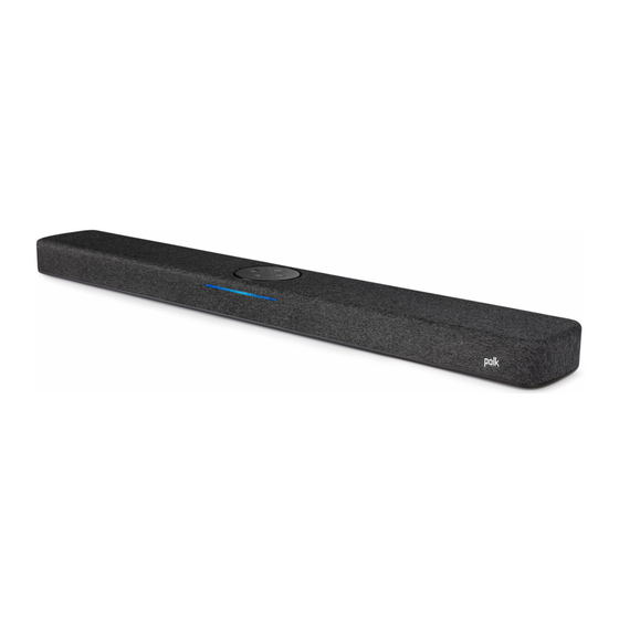
WIRELESS TV SOUND SYSTEM
React
• The parts of this product are not serviceable.
Please replace the product itself.
However, spare parts are available for some parts.
For details, see "PARTS LIST OF EXPLODED VIEW".
Service Manual
Click here!
On-line service parts list
https://dmedia.soundunited.com/documents/details/27899
ONLINE PARTS LIST
(P5)
WEB owner's manual
NA:
http://manuals.polkaudio.com/REACT/NA/EN/index.php
EU:
http://manuals.polkaudio.com/REACT/EU/EN/index.php
JP:
http://manuals.polkaudio.com/REACT/JP/JA/index.php
Upload is planned for the time of a future press release.
BEFORE SERVICING THIS UNIT
ELECTRICAL
MECHANICAL
REPAIR INFORMATION
UPDATING
See Revision History
Confidential
Ver. 2
Advertisement
Table of Contents

Related Manuals for Polk Mono React


Summary of Contents for Polk Mono React
- Page 1 Service Manual Ver. 2 WIRELESS TV SOUND SYSTEM React Click here! On-line service parts list https://dmedia.soundunited.com/documents/details/27899 ONLINE PARTS LIST (P5) WEB owner’s manual http://manuals.polkaudio.com/REACT/NA/EN/index.php http://manuals.polkaudio.com/REACT/EU/EN/index.php http://manuals.polkaudio.com/REACT/JP/JA/index.php Upload is planned for the time of a future press release. BEFORE SERVICING THIS UNIT...
- Page 2 BEFORE SERVICING THIS UNIT SAFETY PRECAUTIONS NOTE FOR SCHEMATIC DIAGRAM HANDLING THE SEMICONDUCTOR AND OPTICS ONLINE PARTS LIST Accessing the Parts List Searching Part Numbers or Ref. Numbers NOTE FOR PARTS LIST SERIAL NUMBER Serial Number Organization SKU Code of this Unit POST-SERVICE PRECAUTIONS Initializing this Unit...
-
Page 3: Safety Precautions
SAFETY PRECAUTIONS The following items should be checked for continued protection of the customer and the service technician. Leakage current check Before returning the set to the customer, be sure to carry out either (1) a leakage current check or (2) a line to chassis resistance check. If the leakage current exceeds 0.5 milliamps, or if the resistance from chassis to either side of the power cord is less than 460 kohms, the set is defective. -
Page 4: Note For Schematic Diagram
NOTE FOR SCHEMATIC DIAGRAM WARNING: Parts indicated by the z mark have critical characteristics. Use ONLY replacement parts recommended by the manufacturer. CAUTION: Before returning the set to the customer, be sure to carry out either (1) a leakage current check or (2) a line to chassis resistance check. -
Page 5: Note For Parts List
ONLINE PARTS LIST Accessing the Parts List Searching Part Numbers or Ref. Numbers (1) Access from the Service Manual You can search a Parts List for part numbers or Ref. numbers. ・ Click the URL link on the cover of the service manual. (1) Enter the part number or Ref. - Page 6 2digit of year serial number SKU Code of this Unit NAV Number Product Name SKU Code NA: 300045-01-00-101 Polk React NA PBDB JP: 300045-01-00-102 Polk React JP PBDC DEMO: 300045-01-00-107 Polk React Demo Config PBDD Global: 300045-01-00-204 Polk React Global Spkr/Device PBDF...
-
Page 7: Initializing This Unit
POST-SERVICE PRECAUTIONS Initializing this Unit The factory reset can be restored at any time. All user data and configuration information are cleared, and the product is restored to the same state as it was when loaded at the factory. The firmware is not downgraded. (1) While the power is On, hold down buttons "Action"... -
Page 8: Schematic Diagrams
ELECTRICAL SCHEMATIC DIAGRAMS SCH01_MAIN01 SCH02_MAIN02 SCH03_MAIN03 SCH04_MAIN04 SCH05_MAIN05 SCH06_MAIN06 SCH07_MAIN07 SCH08_MAIN08 SCH09_MAIN09 SCH10_MAIN10 SCH11_MAIN11 SCH12_MAIN12 SCH13_MAIN13 SCH14_MAIN14 SCH15_MIC01 SCH16_Lamp01 PRINTED CIRCUIT BOARDS MAIN, MIC, Lamp BLOCK DIAGRAM POWER DIAGRAM Remote Code Table... - Page 9 SCHEMATIC DIAGRAMS SCH01_MAIN01 DCDC 5V EN_H>1.5v DCDC 3V9 EN_H>1.5v 01UBUCK1-JW50332 INPUT:4.5-18v INPUT:4.5-18v Vout=0.8*(R_1+R_2)/R_2 Vout=0.8*(R_1+R_2)/R_2 CBT1 Vin : 3.7V<Vin<18V 5V/2A OUT SYS_5V CBT2 STB_3V9 LBT1 4.7uH/3A Vin : 3.7V<Vin<18V LBT2 4.7uH/3A POWER_16V VR300 0.1uF/16V/X7R 0.1uF/16V/X7R VR300 POWER_16V VR300 CBT7 CBT8 CBT3 RBT1 CBT6 CBT4...
- Page 10 SCH02_MAIN02 VR300 HDMI OUT ESD1 NC/ESDPSD2510V05 HDMITX_CLK_M HDMITX_CLK_P SYS_5V HDMI_5V HDMITX_CH0_M HDMITX_CH0_P HDMI_5V clk- clk+ ESD2 NC/ESDPSD2510V05 DAT0- SYS_3V3 HDMITX_CH1_M DAT0+ HDMITX_CH1_P DAT1- DAT1+ 1N4148WS HDMITX_CH2_M DAT2- R1079 HDMITX_CH2_P DAT2+ SHIELD clk shield Dat0 shield Dat1 shield VR300 Dat2 shield HPLG HPLG HDMI_ARC1...
- Page 11 SCH03_MAIN03 Reference 01-POLKNI-MA&IR&WL600 SYS_3V3 SYS_3V3 ADCVDD SYS_1V8 CVDD R1094 R1095 0Ω/0603 C855 C856 DSP_RST R1096 0Ω/0603 nRST C857 C858 C859 C860 C861 C862 nRSTOUT R1097 NC/0 BAT54A PWMVDD R1098 C863 100pF/50V/NP0 C865 C866 C867 C868 PLLVDD R1099 0Ω/0603 C869 C870 4.7uF/6.3V/X5R RVDD 0.1uF/16V/X7R...
- Page 12 SCH04_MAIN04 Reference 01-POLKNI-MA&IR&WL600 SYS_16V 设定的掉电电压根据实际 需 要 调 整 , SYS_3V3 掉 电 检 测 电 压 V=0.6*(R5+R1)/R1 REU1 16V_DET 470uF/25V REU2 PWRDN 16V_DET VCC-Sign SUB-GND C890 C889 10uH/3A OUT3A VCC-Sign OUT2B OUT3A REU3 100K QEU1 REU4 CEU1 C891 0.1uF/50V/X7R 0.1uF/50V/X7R VR300 NC/100K...
- Page 13 SCH05_MAIN05 WIRELESS Main Board TO MIC Board This part is not in the machine by JN SYS_1V8 MPU_1V8 R1198 SYS_3V3 VR400 SYS_3V3_A-1 SYS_3V3_A 0Ω/0603 Surround_LED VR400 Subwoofer_LED VR300 I2C_SDA SYS_A_POWER_CTL C956 C957 I2C_SDA SYS_A_POWER_CTL I2C_SCL SYS_POWER_CTL I2C_SCL SYS_POWER_CTL AMP_OVER 0.1uF/16V/X7R data1 R1242 220Ω/500mA...
- Page 14 SCH06_MAIN06 VCORE_FB VCCK VCORE_PMU DUMMY VCCK DUMMY VCCK DUMMY VCCK AE25 DUMMY VCCK AF25 22uF/6.3V/X5R 22uF/6.3V/X5R 22uF/6.3V/X5R 22uF/6.3V/X5R DUMMY VCCK 100nF/6.3V/X5R 100nF/6.3V/X5R 100nF/6.3V/X5R 4.7uF/6.3V/X5R 1uF/6.3V/X5R VCCK VCCK VCCK VCCK VCCK GND_VCORE_FB VCCK VCCK VCCK VCCK VCCK VPROC_FB GNDK GNDK VCCK_VPROC GNDK VCCK_VPROC VPROC_PMU...
- Page 15 SCH07_MAIN07 I2S_8CH_LRCK I2S_8CH_LRCK_1 NC/5.6pF/50V/NP0 I2S_8CH_BCK I2S_8CH_BCK_1 R939 C837 5.6pF/50V/NP0 WATCHDOG SYSRSTB WDTRSTB_IN WATCHDOG SYSRSTB SYSRSTB RTC32K_CK RTC32K_1V8 SRCLKENA RTC32K_CK SRCLKENA TESTMODE 100nF/6.3V/X5R PWRAP_SPI0_CK TESTMODE PWRAP_SPI0_CK 100nF/6.3V/X5R PWRAP_SPI0_CSN PWRAP_SPI0_CSN PWRAP_SPI0_MO PWRAP_SPI0_MO URXD0_RX URXD0 PWRAP_SPI0_MI PWRAP_SPI0_MI URXD0 VELDO18_PMU PWRAP_INT PWRAP_INT FSOURCE_P AC14 FSOURCE_P EINT0 GPIO0...
- Page 16 SCH08_MAIN08 VBAT 2.2uF/6.3V/X5R VBAT_SPK VBAT_SPK VBUS AUDIO GND_SPK SPK_P SPK_N VCDT rating: 1.268V From 8516 >>> CLK_IN_26MHZ CLK_IN_26MHZ CLKO_26M CLK_IN_26MHZ 330K_1% VCDT R287 near R297 footprint:SWPA252012S-L 0402-R CHARGER BUCK OUTPUT VPROC_LX 39K_1% VBAT VPROC_PMU BATSNS VPROC_LX 0201-R L/680nH/3.62A/VLS252010HBX-R68M VPROC_LX 1uF/6.3V/X5R ISENSE 1uF/6.3V/X5R 80mil...
- Page 17 SCH09_MAIN09 ED16 ED17 ED23 ED21 ED22 ED19 ED18 ED20 ED24 ED31 ED26 EA10 DQ10 A10/AP ED27 EA11 DQ11 ED28 EA12 DQ12 A12/BC# ED25 EA13 ED10 DQ13 ED30 EA14 ED11 DQ14 ED29 EA15 ED12 DQ15 For dual rank ED13 ECS1 ED14 CS1# EDQS3 ZQ1_B...
- Page 18 SCH10_MAIN10 AVSS_CONN AVDD18_WBT AVSS_CONN AVDD18_WBT_AFE AVSS_CONN AVSS_CONN AVSS_CONN AVSS_CONN AVSS_CONN AVSS_CONN AVSS_CONN AVSS_CONN AVDD33_WBT AVSS_CONN AVSS_CONN AA10 AVSS_CONN AVSS_CONN AVSS_CONN AVSS_CONN AVSS_CONN AVSS_CONN AVSS_CONN WBT_EXT_G AB10 AVSS_CONN WB_RFIN AVSS_CONN AVSS_CONN AVSS_CONN AVSS_CONN AVSS_CONN GPS_DPX_RFOUT AVDD22_XO AB23 VXO22_PMU AVDD22_XO 470nF/6.3V/X5R 26M_XO_IN AC25 XO_IN AB25...
- Page 19 SCH11_MAIN11 BUCK_1V3_OUT from pin18 3.3V_A Vout = 0.6* (1 + R16/R21) = 3.4V 50 Ohm RFIP_BT RFIP_BT C180 C125 WIFI_3.3V 3.3V_A VBAT 0.1uF/6.3V/X5R 10pF/50V/NPO R125 R123 1uH/3.18A C126 1uF/6.3V/X5R C106 C108 C104 VIO18_PMU VIO18_PMU0 VIO18_PMU1 DVDD11 10uF/16V/X5R 0.1uF/16V/X7R 10UF/6.3V/X5R 0.1uF/16V/X7R from 6392 220Ω/500mA from pin22.23...
-
Page 20: Nand Flash
SCH12_MAIN12 3.3V_NAND EINT14 NCLE EINT14 EINT15 500/800mA VEMC_3V3_PMU EINT16 NCEB0 eMMC_DAT7 EINT16 C138 MSDC0_DAT7 NLD7 4.7uF/6.3V/X5R MSDC0_DAT7 EINT17 NREB EINT17 0402-C eMMC_DAT6 EINT21 NRNB EINT21 MSDC0_DAT6 NLD6 MSDC0_DAT6 EINT22 eMMC_DAT5 MSDC0_DAT5 NLD4 EINT23 MSDC0_DAT5 eMMC_DAT4 MSDC0_DAT4 NLD3 MSDC0_DAT4 eMMC_RST MSDC0_RSTB NLD0 MSDC0_RSTB eMMC_CMD... - Page 21 SCH13_MAIN13 HDMITX_CH0_M HDMITX_CH0_M HDMITX_CH0_M AD22 HDMITX_CH0_P HDMITX_CH0_M HDMITX_CH0_P HDMITX_CH0_P AC22 HDMITX_CH0_P HDMITX_CH1_M HDMITX_CH1_M HDMITX_CH1_M AE23 HDMITX_CH1_P HDMITX_CH1_M HDMITX_CH1_P HDMITX_CH1_P AD23 HDMITX_CH1_P HDMITX_CH2_M AE24 HDMITX_CH2_M HDMITX_CH2_M HDMITX_CH2_M HDMITX_CH2_P AD24 HDMITX_CH2_P HDMITX_CH2_P HDMITX_CH2_P HDMITX_CLK_M AC21 HDMITX_CLK_M HDMITX_CLK_M HDMITX_CLK_P HDMITX_CLK_M AB21 HDMITX_CLK_P HDMITX_CLK_P HDMITX_CLK_P AF22 HDMITX_REXT...
- Page 22 SCH14_MAIN14 USB_OTG_PWR_EN I2C_SCL0 TP81 AMP_I2C_SCL I2C_SDA0 AMP_I2C_SDA I I C ( 外 部 上 拉 3 . 3 V ) I2C_SCL1 MCU_I2C_SCL I2C_SDA1 SPI0_MISO MCU_I2C_SDA TP80 SPI0_MOSI I2C_SDA3 TP77 DSP_I2C_SDA GPIO0 I2C_SCL3 TP78 GPIO24 DSP_I2C_SCL TP79 SPI0_MISO TP74 DSP_SPI0_MISO SPI0_MOSI TP75 DSP SPI DSP_SPI0_MOSI...
- Page 23 SCH15_MIC01 D1V8 D1V8 MIC&ADC R501 MIC1_BIAS1 C161 1uF/6.3V/X5R C162 1uF/6.3V/X5R NC/0 C163 MSM381A3526Z9BMC C165 NC/15pF/50V/NP0 100nF/6.3V/X5R C164 100nF/6.3V/X5R DIR1_P R203 C166 1uF/6.3V/X5R MIC_MCLK1 R496 NC/0 R502 MIC_3V3 C168 ESD8 ESD9 A D C M C L K 可 可 可可 可B C L K 转 转 47nF/10V/X5R C170 NC/0...
- Page 24 SCH16_Lamp01 LED_5V RGB_5V R256 R257 C229 C240 C241 LED_5V LED_5V IIC Add:7E U20B LED5 C231 R258 R267 C230 LED_RGB 4.7K LED_SDA1 LED6 LED_SCL1 R_EXT LED_SDB1 LED_RGB R259 7.5K LED_RGB Imax=58.5*1.3V/Rext LED7 GND1 GND2 R260 =10mA C242 U20A NC/100K LED8 IS31FL3236A OUT1 OUT36 LED_RGB...
- Page 25 PRINTED CIRCUIT BOARDS Lead-free Solder When soldering, use the Lead-free Solder (Sn-Ag-Cu). MAIN, MIC, Lamp MAIN (A Side) MAIN (B Side) R1131 R1130 R1135 R1136 R1138 R1137 R1128 R1120 R1152 R1150 R1151 R1148 R1129 C1001 TP67 TP68 R1154 R1126 TM21 TM20 R1132 R1125...
-
Page 26: Block Diagram
BLOCK DIAGRAM Module Flash DDR3 512MB 256MB(U3) (U7) OSC26M0N BT/WIFI SDIO RGB Driver MT7668(U25 IIC1 (X3/26.0M RGB*12 IS31FL3236 ,2.4G/5.8G) (U20) MT6392(U2) IIC1 HX3203 TDM_IIS TLV320AD (U16) MIC*4 TDM_Data C3101*2 Green LEDx2, Red LEDx2 (U14,U18) D+/D- OSC26M0N4FT (X2/26.0MHz) GPIO*4 SR+SL KEY*4 MT8516 IIS0 Data0... -
Page 27: Power Diagram
POWER DIAGRAM Working Current distribu�on diagram(Bar) Module VPROC_1.35V VCore_1.15V VAUD28_PMU VAUD22_PMU VADC18_PMU VXO22_PMU MT6392 VIO18_PMU VEMC_3V3_NAND&I2S VMC_PMU_3V3 I2S VUSB33_PMU DDR_1.35V SY8120I WIFI_3.3V TLV62569 η =85% SY8120I η =85% SY8088I JSA-1130 STA518*2 HDMI STA518 RGB*12+LED*2 Optical IA9QH5 TLV62 TLV320AD OTHER C3101*2 TLV320 SGM8061 ADC310... - Page 28 Remote Code Table Name Button Code Located on Remote? 1 Alexa C891 AA55 2 Mute (toggle) C891 20DF 3 TV INPUT C891 0FF0 4 Bluetooth C891 0AF5 5 Volume Up C891 1EE1 6 Volume Down C891 1FE0 7 Bass Up C891 5CA3 8 Bass Down C891 5DA2...
- Page 29 MECHANICAL EXPLODED VIEW PACKAGING VIEW...
-
Page 30: Exploded View
EXPLODED VIEW https://dmedia.soundunited.com/documents/details/27899 Parts List : M1 x4 WARNING: Parts marked with this symbol z have critical characteristics. Use ONLY replacement parts recommended by the manufacturer. - Page 31 PACKAGING VIEW https://dmedia.soundunited.com/documents/details/27899 Parts List : P5-1 P5-2 UK AC Adapter (Put this by SU after shipment)
-
Page 32: Repair Information
REPAIR INFORMATION TROUBLE SHOOTING SPECIAL MODE Special mode setting button 1. Version Display Mode 2. Factory Reset Mode 3. Log Submission Mode 4. Locale settings and confirmation... -
Page 33: Troubleshooting
TROUBLE SHOOTING Repair service is not available for this unit. To repair, reset the unit and update the software. If it still does not recover, replace the unit with a new one. -
Page 34: Special Mode Setting Button
SPECIAL MODE Special mode setting button b No. 1 : While the power is on, hold down buttons "A", "B", and "C" for at least 5 seconds . b No. 2 : While the power is on, hold down buttons "A" for at least 25 seconds . b No. -
Page 35: Version Display Mode
1. Version Display Mode 2. Factory Reset Mode 1.1. Actions The factory reset can be restored at any time. All user data and configuration information are cleared, and the product is restored to the same state as it was when loaded at the factory. Version information is displayed when the device is started in this mode. - Page 36 4.2. Locale confirmation 4. Locale settings and confirmation 4.1. Creating the locale settings and confirmation file (1) Insert the AC plug and turn on the power. (1) Click [Start button] - [Accessories] - [notepad] on the PC to launch the notepad. •...
-
Page 37: Firmware Update Procedure
UPDATING FIRMWARE UPDATE PROCEDURE 1. Items necessary for update 2. Updating via Network 3. Updating via USB... - Page 38 FIRMWARE UPDATE PROCEDURE 1. Items necessary for update Items necessary for update are as follows. Offered / not Offered Update Type Needed Part for Update Requirement Standard Service Equipment Purchase from D&M Article code Download from SDI Not offered by D&M Smart phone Internet Connection Via OTA...
-
Page 39: Items To Be Prepared
2. Updating via Network You can update the firmware by downloading the latest version via network. 2.1. Items to Be Prepared • Smart phone • Broadband Internet connection • Modem • Router • Ethernet cable (CAT-5 or greater is recommended) 2.2. -
Page 40: Updating Via Usb
3. Updating via USB You can update the firmware by downloading the latest version with USB flash drive. The USB update is always executed regardless of the currently installed version or the version of the USB flash drive. Thus, old versions, the same version or new versions can be installed from the USB flash drive. 3.1. -
Page 41: Revision History
Revision History Ver Page Description Before the change After the change Date Addition of Item. 3. Log Submission Mode 23, Apr. 2021 No. 3 : While the power is on and the unit is connected to the Internet, Addition the document. hold down buttons "A"... - Page 42 www.polkaudio.com ©2020-2021 Sound United. All Rights Reserved.
Need help?
Do you have a question about the React and is the answer not in the manual?
Questions and answers