
Related Manuals for Asus AAEON GENE-SKU6


Summary of Contents for Asus AAEON GENE-SKU6
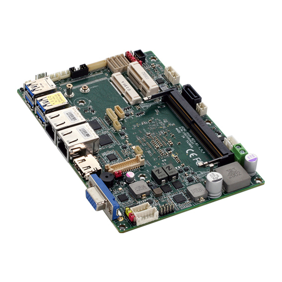
- Page 1 GENE-SKU6 3.5” Subcompact Board User ’s Manual 13 Last Updated: October 28, 2021...
- Page 2 Copyright Notice This document is copyrighted, 2021. All rights are reserved. The original manufacturer reserves the right to make improvements to the products described in this manual at any time without notice. No part of this manual may be reproduced, copied, translated, or transmitted in any form or by any means witho ut the prior written permission of the original manufacturer.
- Page 3 Acknowledgement All other products’ name or trademarks are properties of their respective owners. Microsoft Windows is a registered trademark of Microsoft Corp. ⚫ Intel® and Celeron® are registered trademarks of Intel Corporation ⚫ Intel Core™ is a trademark of Intel Corporation ⚫...
- Page 4 Packing List Before setting up your product, please make sure the following items have been shipped: I t em Quantity GENE-SKU6 MB Heat Spreader If any of these items are missing or damaged, please contact your distributor or sales representative immediately. Preface...
- Page 5 About this Document This User’s Manual contains all the essential information, such as detailed descriptions and explanations on the product’s hardware and software features (if any), its specifications, dimensions, jumper/connector settings/definitions, and driver installation instructions (if any), to facilitate users in setting up their product. Users may refer to the product page at AAEON.com for the latest version of this document.
- Page 6 Saf e ty Precautions Please read the following safety instructions carefully. It is advised that you keep this manual for future references All cautions and warnings on the device should be noted. Make sure the power source matches the power rating of the device. Position the power cord so that people cannot step on it.
- Page 7 If any of the following situations arises, please the contact our service personnel: Damaged power cord or plug Liquid intrusion to the device iii. Exposure to moisture Device is not working as expected or in a manner as described in this manual The device is dropped or damaged Any obvious signs of damage displayed on the device...
- Page 8 FCC Statement This device complies with Part 15 FCC Rules. Operation is subject to the following two conditions: (1) this device may not cause harmful interference, and (2) this device must accept any interference received including interference that may cause undesired operation.
- Page 9 Chi na RoHS Requirements ( CN) 产品中有毒有害物质或元素名称及含量 AAEON Main Board/ Daughter Board/ Backplane 有毒有害物质或元素 部件名称 铅 汞 镉 六价铬 多溴联苯 多溴二苯醚 (Pb) (Hg) (C d) (C r(VI)) (PBB) (PBDE) 印刷电路板 ○ ○ ○ ○ ○ ○ 及其电子组件 外部信号 ○ ○ ○...
- Page 10 Chi na RoHS Requirement (EN) Poisonous or Hazardous Substances or Elements in Products AAEON Main Board/ Daughter Board/ Backplane Poisonous or Hazardous Substances or Elements He xavalent Polybrominated Polybrominated C omponent Le ad Me rcury C admium C hromium Biphenyls Diphenyl Ethers (Pb) (Hg)
-
Page 11: Table Of Contents
Table of Contents Chapter 1 - Product Specifications..............1 Specifications .................... - Page 12 2.4.8 LAN (RJ-45) Port2 (CN10) .............21 2.4.9 Mini- Card Slot (Full-Mini Card) (CN11) ........22 2.4.10 Micro SIM Card Socket (CN12) ............ 24 2.4.11 Mini- Card Slot (Half-Mini Card) (CN13) ........25 2.4.12 SATA Port 1 (CN14) ............... 27 2.4.13 +5V Output for SATA HDD (CN15)..........
- Page 13 Chapter 3 - AMI BIOS Setup..............60 System Test and Initialization ................61 AMI BIOS Setup ....................
- Page 14 Chapter 4 – Drivers Installation ..............95 Driver Download/Installation ...............
-
Page 15: Chapter 1 - Product Specifications
Chapter 1 Chapter 1 - Product Specifications... -
Page 16: Specifications
1 .1 Spe cifications System F o rm Factor 3.5'' Sub-Compact Board CP U 6th Generation Intel® Core™/ Celeron® Processor: Core i7-6600U (2C/4T 2.60 GHz, up to 3.40 GHz) Core i5-6300U (2C/4T 2.40 GHz, up to 3.00 GHz) Core i3-6100U (2C/4T, 2.30 GHz) Celeron®... - Page 17 Powe r Po wer Consumption (Typical) 3.42A at +12V with Intel® Core™ i7-6600U, DDR4 2666MHz 32GB Po wer Consumption (Max) 4.25A at +12V with Intel® Core™ i7-6600U, DDR4 2666MHz 32GB Di splay Co ntroller Intel® HD Graphics 520/610 LVDS/eDP LVDS Dual Channel 18/24-bit x 1 Dis play Interface DP1.2 x 1 + DVI-D x 1 (default) Optional: DVI-I x 1 (with VGA signal)
- Page 18 Internal I/O U SB USB2.0 x 2 Serial Port COM1 (RS232) COM2, COM3, COM4 (RS232/422/485, supports 5V/12V/RI Vid eo LVDS x 1 SATA SATA III (6.0 Gbps) x 1 +5V SATA Power Connector x 1 A ud io Audio Header x 1 DI O/GPIO 8-bit SMB us/ I2C...
-
Page 19: Block Diagram
E nvironment Op erating Humidity 0% ~ 90% relative humidity, non-condensing MTBF (Hours) 375,577 EMC Certification CE/FCC Class A 1 .2 Bl ock Diagram Chapter 1 – Product Specifi c ations... -
Page 20: Chapter 2 - Hardware Information
Chapter 2 Chapter 2 – Hardware Information... -
Page 21: Dimensions
Di mensions Co mponent Side Component Side Chapter 2 – Hardware Information... - Page 22 So lder Side (with heat spreader) Solder Side Chapter 2 – Hardware Information...
-
Page 23: Jumpers And Connectors
2.2 Jum pers and Connectors Component Side Chapter 2 – Hardware Information... -
Page 24: List Of Jumpers
2.3 Li st of Jumpers Please refer to the table below for all of the board’s jumpers that you can configure for your application Lab el F unction JP 1 Clear CMOS Jumper JP 2 LVDS Port Backlight Inverter VCC Selection JP 3 LVDS Port Backlight Lightness Control Mode Selection JP 4... -
Page 25: Lvds Port Backlight Lightness Control Mode Selection (Jp3)
2.3.3 LVDS Port Backlight Lightness Control Mode Selection ( JP3) VR Mode (Default) PWM Mode 2.3 .4 LVDS Port Operating VDD Selection ( JP4) 1 2 3 +3.3V (Default) 2.3 .5 mSATA/ Mini-Card Operating VCC Selection (JP5) mSATA (Default) Mini-Card 2.3 .6 Touch Screen 4,5,8 Wire Selection (JP6) 4/8 Wire Mode (Default) -
Page 26: Com3 Pin8 Funct Ion Selection (Jp8)
2.3 .8 COM3 Pin8 Function Selection ( JP8) Ring (Default) +12V 2.3 .9 COM2 Pin8 Function Selection ( JP9) Ring (Default) +12V 2.3 .10 Front Panel Connector (JP10) P in P in Name P in P in Name PWR_BTN- PWR_BTN+ HDD_LED- HDD_LED+ SPEAKER-... -
Page 27: Com4 Pin8 Function Selection (Jp11)
2.3 .11 COM4 Pin8 Function Selection ( JP11) Ring (Default) +12V Chapter 2 – Hardware Information... -
Page 28: List Of Connectors
2.4 Li st of Connectors Please refer to the table below for all of the board’s connectors that you can configure for your application Lab el F unction CN 1 Battery CN 3 DVI-I (Digital and Analog) CN 5 DP Port CN 6 LVDS Port CN 7... -
Page 29: Battery (Cn1)
Lab el F unction CN 28 COM Port 3 CN 29 LPC Port CN 30 External Power Input CN 32 +5VSB Output w/SMBus CN 33 External +5VSB Input CN 35 BIO Connector CN 36 CPU FAN 2.4.1 Battery (CN1) P in P in Name Sig nal Type Sig nal Level... -
Page 30: Dp Port (Cn5)
P in P in Name Sig nal Type Sig nal Level DVI_D0- DVI_D0+ DVI_CLK+ DVI_CLK- VGA_RED VGA_GREEN VGA_BLUE VGA_HSYNC 2.4.3 DP Por t (CN5) P in P in Name Sig nal Type Sig nal Level DP_D0+ DIFF DP_D0- DIFF DP_D1+ DIFF Chapter 2 –... - Page 31 P in P in Name Sig nal Type Sig nal Level DP_D1- DIFF DP_D2+ DIFF DP_D2- DIFF DP_D3+ DIFF DP_D3- DIFF DP_AUX+ DIFF DP_AUX- DIFF HPLG_DETECT Chapter 2 – Hardware Information...
-
Page 32: Lvds Port (Cn6)
2.4.4 LVDS Port ( CN6) N o te: LVDS LCD_PWR can be set to +3.3V or +5V by JP4. Driving Current supports up to 1.5A P in P in Name Sig nal Type Sig nal Level BKL_ENABLE BKL_CONTROL LCD_PWR +3.3V/+5V LVDS_A_CLK- DIFF LVDS_A_CLK+... -
Page 33: Lvds Port Inverter / Backlight Connector (Cn7)
P in P in Name Sig nal Type Sig nal Level LVDS_DA3- DIFF LVDS_DA3+ DIFF DDC_DATA +3.3V DDC_CLK +3.3V LVDS_DB0- DIFF LVDS_DB0+ DIFF LVDS_DB1- DIFF LVDS_DB1+ DIFF LVDS_DB2- DIFF LVDS_DB2+ DIFF LVDS_DB3- DIFF LVDS_DB3+ DIFF LCD_PWR +3.3V/+5V LVDS_B_CLK- DIFF LVDS_B_CLK+ DIFF 2.4.5 LVDS Port Inverter / Backlight Connector ( CN7) -
Page 34: Spi Debug Port (Cn8)
P in P in Name Sig nal Type Sig nal Level BKL_ENABLE N o te 1: LVDS BKL_PWR can be set to +5V or +12V by JP2. Driving current supports up to 2A. N o te 2: LVDS BKL_CONTROL can be set by JP3 2.4.6 SPI Debug Port ( CN8) P in... -
Page 35: Lan (Rj-45) Port1 (Cn9)
2.4.7 L AN ( RJ-45) Port1 ( CN9) P in P in Name Sig nal Type Sig nal level MDI0+ DIFF MDI0- DIFF MDI1+ DIFF MDI2+ DIFF MDI2- DIFF MDI1- DIFF MDI3+ DIFF MDI3- DIFF 2.4.8 L AN ( RJ-45) Port2 ( CN10) P in P in Name Sig nal Type... -
Page 36: Mini- Card Slot (Full-Mini Card) (Cn11)
P in P in Name Sig nal Type Sig nal level MDI2+ DIFF MDI2- DIFF MDI1- DIFF MDI3+ DIFF MDI3- DIFF 2.4.9 Mi ni-Card Slot ( Full-Mini Card) ( CN11) P in P in Name Sig nal Type Sig nal Level PCIE_WAKE# +3.3VSB +3.3V... - Page 37 P in P in Name Sig nal Type Sig nal Level W_DISABLE# +3.3V PCIE_RST# +3.3V PCIE_RX- DIFF +3.3VSB +3.3V PCIE_RX+ DIFF +1.5V +1.5V SMB_CLK +3.3V PCIE_TX- DIFF SMB_DATA +3.3V PCIE_TX+ DIFF USB_D- DIFF USB_D+ DIFF +3.3VSB +3.3V +3.3VSB +3.3V Chapter 2 – Hardware Information...
-
Page 38: Micro Sim Card Socket (Cn12)
P in P in Name Sig nal Type Sig nal Level +1.5V +1.5V +3.3VSB +3.3V 2.4.10 Mi cro SIM Card Socket ( CN12) P in P in Name Sig nal Type Sig nal Level UIM_PWR UIM_RST UIM_CLK UIM_VPP UIM_DATA Chapter 2 – Hardware Information... -
Page 39: Mini- Card Slot (Half-Mini Card) (Cn13)
2.4.11 Mi ni-Card Slot ( Half-Mini Card) (CN13) P in P in Name Sig nal Type Sig nal Level PCIE_WAKE# +3.3VSB +3.3V +1.5V +1.5V PCIE_CLK_REQ# PCIE_REF_CLK- DIFF PCIE_REF_CLK+ DIFF W_DISABLE# +3.3V PCIE_RST# +3.3V PCIE_RX-/mSATA_RX+ DIFF +3.3VSB +3.3V Chapter 2 – Hardware Information... - Page 40 P in P in Name Sig nal Type Sig nal Level PCIE_RX+/mSATA_RX- DIFF +1.5V +1.5V SMB_CLK +3.3V PCIE_TX-/mSATA_TX- DIFF SMB_DATA +3.3V PCIE_TX+/mSATA_TX+ DIFF USB_D- DIFF USB_D+ DIFF +3.3VSB +3.3V +3.3VSB +3.3V +1.5V +1.5V Chapter 2 – Hardware Information...
-
Page 41: Sata Port 1 (Cn14)
P in P in Name Sig nal Type Sig nal Level +3.3VSB +3.3V N o te: CN13 can be selected for Mini-Card or mSATA by changing BIOS 2.4.12 SATA Port 1 ( CN14) P in P in Name Sig nal Type Sig nal Level SATA_TX+ DIFF... -
Page 42: Output For Sata Hdd (Cn15)
2.4.13 +5V Output for SATA HDD (CN15) P in P in Name Sig nal Type Sig nal Level N o te: +5V Output for SATA HDD, driving current supports up to 1A 2.4.14 USB 3.0 Ports (CN18) P in P in Name Sig nal Type Sig nal Level +5VSB... -
Page 43: Usb 3.0 Ports (Cn19)
P in P in Name Sig nal Type Sig nal Level USB_SSTX− DIFF USB_SSTX+ DIFF +5VSB USB_D- DIFF USB_D+ DIFF USB_SSRX− DIFF USB_SSRX+ DIFF USB_SSTX− DIFF USB_SSTX+ DIFF N o te: USB3.0 Ports support current up to 0.9A 2.4.15 USB 3.0 Ports (CN19) Port 1 11 12 13 Port 0... - Page 44 P in P in Name Sig nal Type Sig nal Level USB_SSRX− DIFF USB_SSRX+ DIFF USB_SSTX− DIFF USB_SSTX+ DIFF +5VSB USB_D- DIFF USB_D+ DIFF USB_SSRX− DIFF USB_SSRX+ DIFF USB_SSTX− DIFF USB_SSTX+ DIFF N o te: USB3.0 Ports support current up to 0.9A Chapter 2 –...
-
Page 45: Usb 2.0 Port (Cn20)
2.4.16 USB 2.0 Port (CN20) P in P in Name Sig nal Type Sig nal Level +5VSB USB_D- DIFF USB_D+ DIFF N o te: USB2.0 Ports support current up to 0.5A 2.4.17 USB 2.0 Port (CN21) P in P in Name Sig nal Type Sig nal Level +5VSB... -
Page 46: Audio I/O Port (Cn22)
2.4.18 Audi o I/O Port (CN22) P in P in Name Sig nal Type Sig nal Level MIC_L MIC_R GND_AUDIO LINE_L_IN LINE_R_IN GND_AUDIO LEFT_OUT GND_AUDIO RIGHT_OUT +5V_AUDIO Chapter 2 – Hardware Information... -
Page 47: Touchscreen Connector (Cn23)
2.4.19 Touchscreen Connector (CN23) N o te: Touch mode can be set by JP6 4- wire Mode: P in P in Name Sig nal Type Sig nal Level BOTTOM LEFT RIGHT Chapter 2 – Hardware Information... - Page 48 5- wire Mode P in P in Name Sig nal Type Sig nal Level UL(Y) UR(H) LL(L) LR(X) SENSE(S) Chapter 2 – Hardware Information...
- Page 49 8- wire Mode P in P in Name Sig nal Type Sig nal Level TOP EXCITE BOTTOM EXCITE LEFT EXCITE RIGHT EXCITE TOP SENSE BOTTOM SENSE LEFT SENSE RIGHT SENSE Chapter 2 – Hardware Information...
-
Page 50: Digital I/O Port (Cn24)
2.4.20 Di gital I/O Port (CN24) P in P in Name Sig nal Type Sig nal Level DIO0 DIO1 DIO2 DIO3 DIO4 DIO5 DIO6 DIO7 N o te: Digital I/O port supports current up to 0.5A Chapter 2 – Hardware Information... -
Page 51: Com Port 1 (Cn25)
2.4.21 COM Port 1 ( CN25) P in P in Name Sig nal Type Sig nal Level ±9V ±9V ±9V Chapter 2 – Hardware Information... -
Page 52: Com Port 4 (Cn26)
2.4.22 COM Port 4 (CN26) R S-232 Mode RI/+5V/+12V P in P in Name Sig nal Type Sig nal Level ±5V ±5V ±5V RI/+5V/+12V IN/ PWR +5V/+12V Chapter 2 – Hardware Information... - Page 53 R S-422 Mode RS422_TX- RS422_TX+ RS422_RX+ RS422_RX- NC/+5V/+12V P in P in Name Sig nal Type Sig nal Level RS422_TX- ±5V RS422_TX+ ±5V RS422_RX+ RS422_RX- NC/+5V/+12V +5V/+12V Chapter 2 – Hardware Information...
- Page 54 R S-485 Mode P in P in Name Sig nal Type Sig nal Level RS485_D- ±5V RS485_D+ ±5V NC/+5V/+12V +5V/+12V N o te 1: COM4 RS-232/422/485 can be set by BIOS. Default is RS-232. N o te 2: Pin 8 function can be set by JP11. Maximum driving current in power supply mode is 0.5A Chapter 2 –...
-
Page 55: Com Port 2 (Cn27)
2.4.23 COM Port 2 ( CN27) R S-232 Mode RI/+5V/+12V P in P in Name Sig nal Type Sig nal Level ±5V ±5V ±5V RI/+5V/+12V IN/ PWR +5V/+12V Chapter 2 – Hardware Information... - Page 56 R S-422 Mode RS422_TX- RS422_TX+ RS422_RX+ RS422_RX- NC/+5V/+12V P in P in Name Sig nal Type Sig nal Level RS422_TX- ±5V RS422_TX+ ±5V RS422_RX+ RS422_RX- NC/+5V/+12V +5V/+12V Chapter 2 – Hardware Information...
- Page 57 R S-485 Mode P in P in Name Sig nal Type Sig nal Level RS485_D- ±5V RS485_D+ ±5V NC/+5V/+12V +5V/+12V N o te 1: COM2 RS-232/422/485 can be set by BIOS setting. Default is RS-232. N o te 2: Pin 8 function can be set by JP9. Maximum driving current in power supply mode is 0.5A Chapter 2 –...
-
Page 58: Com Port 3 (Cn28)
2.4.24 COM Port 3 ( CN28) R S-232 Mode RI/+5V/+12V P in P in Name Sig nal Type Sig nal Level ±5V ±5V ±5V RI/+5V/+12V IN/ PWR +5V/+12V Chapter 2 – Hardware Information... - Page 59 R S-422 Mode RS422_TX- RS422_TX+ RS422_RX+ RS422_RX- NC/+5V/+12V P in P in Name Sig nal Type Sig nal Level RS422_TX- ±5V RS422_TX+ ±5V RS422_RX+ RS422_RX- NC/+5V/+12V +5V/+12V Chapter 2 – Hardware Information...
- Page 60 R S-485 Mode P in P in Name Sig nal Type Sig nal Level RS485_D- ±5V RS485_D+ ±5V NC/+5V/+12V +5V/+12V N o te 1: COM3 RS-232/422/485 can be set by BIOS setting. Default is RS-232. N o te 2: Pin 8 function can be set by JP8. Maximum driving current in power supply mode is 0.5A Chapter 2 –...
-
Page 61: Lpc Port (Cn29)
2.4.25 LPC Port ( CN29) P in P in Name Sig nal Type Sig nal Level LAD0 +3.3V LAD1 +3.3V LAD2 +3.3V LAD3 +3.3V +3.3V +3.3V LFRAME# LRESET# +3.3V LCLK I2C_SDA I2C_SCL SERIRQ +3.3V Chapter 2 – Hardware Information... -
Page 62: External Power Input (Cn30)
2.4.26 E xternal Power Input ( CN30) P in P in Name Sig nal Type Sig nal Level +12V +9~+36V (or +12V) Note: Pin 1/ Vin maximum current rating is 7A. 2.4.27 +5VSB Output w/SMBus (CN32) SMB_DATA SMB_CLK PS_ON# +5VSB P in P in Name Sig nal Type... -
Page 63: External +5Vsb Input (Cn33)
2.4.28 E xternal +5VSB Input ( CN33) P in P in Name Sig nal Type Sig nal Level PS_ON# +3.3V +5VSB N o te: Maximum current rating of Pin#3/+5VSB is 2A 2.4.29 BIO Connector (CN35) P in P in Name Sig nal Type Sig nal Level +12V_Dual... - Page 64 P in P in Name Sig nal Type Sig nal Level PCIE2_RX- PCIE2_TX+ PCIE2_RX+ PS_ON# +5V_Dual +5V_Dual +5V_Dual +5V_Dual PCIE_CLK+ PLT_RST# PCIE_CLK- Chapter 2 – Hardware Information...
- Page 65 P in P in Name Sig nal Type Sig nal Level USB 3.0_TX- USB 3.0_TX+ USB 2.0_D- USB 2.0_D+ USB 3.0_RX- USB 3.0_RX+ SMB_CLK SMB_DATA PCIE_WAKE# USB 2.0_OC# USB 2.0_OC# Chapter 2 – Hardware Information...
- Page 66 P in P in Name Sig nal Type Sig nal Level LPC_AD0 LPC_FRAME# LPC_AD1 SERIRQ# LPC_AD2 LPC_AD3 GPIO Audio_GND LPC_CLK Audio_OUT_L PME# Audio_OUT_R Chapter 2 – Hardware Information...
-
Page 67: Cpu Fan (Cn36)
2.4.30 CPU Fan (CN36) P in P in Name Sig nal Type Sig nal Level FAN_POWER +12V FAN_TAC FAN_CTL +3.3V N o te: +12V Output for FAN power. Driving current supports up to 2A Chapter 2 – Hardware Information... -
Page 68: Thermal Solution
2.5 T he rmal Solution 2.5.1 G E NE-SKU6-HSK01 Heatsink used with heat spreader. Recommend to be used with the system cooler with air flow greater than 7 ft /min. Chapter 2 – Hardware Information... -
Page 69: Gene-Sku6-Hsk02
2.5.2 G E NE-SKU6-HSK02 Single-piece heatsink – does not require a heat spreader. Extended temperature SKUs are tested using the GENE-SKU6-HSK02 thermal solution and under UEFI mode. Chapter 2 – Hardware Information... - Page 70 GEN E-SKU6-HSK02 Assembly Chapter 2 – Hardware Information...
-
Page 71: Gene-Sku6-Fan01
2.5.3 G E NE-SKU6-FAN01 Cooler used with heat spreader. Chapter 2 – Hardware Information... - Page 72 GEN E-SKU6-FAN01 Assembly Chapter 2 – Hardware Information...
-
Page 73: Gene-Sku6-Hsk03
2.5.4 G E NE-SKU6-HSK03 Heatsink for DRAM. Chapter 2 – Hardware Information... -
Page 74: Chapter 3 - Ami Bios Setup
Chapter 3 Chapter 3 - AMI BIOS Setup... -
Page 75: System Test And Initialization
System Test and Initialization The board uses certain routines to perform testing and initialization during the boot up sequence. If an error, fatal or non-fatal, is encountered, the system will output a few short beeps or an error message. The board can usually continue the boot up sequence with non-fatal errors. -
Page 76: Ami Bios Setup
3.2 AMI BIOS Setup The AMI BIOS ROM has a pre-installed Setup program that allows users to modify basic system configurations, which is stored in the battery-backed CMOS RAM and BIOS NVRAM so that the information is retained when the power is turned off. To enter BIOS Setup, press <Del>... -
Page 77: Setup Submenu: Main
3.3 Se tup Submenu: Main Chapter 3 – AMI BIOS Setup... -
Page 78: Setup Submenu: Advanced
3.4 Se tup Submenu: Advanced Chapter 3 – AMI BIOS Setup... -
Page 79: Cpu Configuration
3.4.1 CPU Configuration Op tions Summary A ctive Processor Cores Optimal Default, Failsafe Default Number of cores to enable in each processor package. I nt el (VMX) Virtualization Disabled Technology Enabled Optimal Default, Failsafe Default When enabled, a VMM can utilize the additional hardware capabilities provided by Vanderpool Technology. -
Page 80: Trusted Computing
3.4.2 Trusted Computing Op tions Summary Security Device Support Disable Enable Optimal Default, Failsafe Default Enables or Disables BIOS support for security device. O.S. will not show Security Device. TCG EFI protocol and INT1A interface will not be available. SHA-1 PCR Bank Disable Enable Optimal Default, Failsafe Default... - Page 81 Op tions Summary P latform Hierarchy Disable Enable Optimal Default, Failsafe Default Enable or Disable Platform Hierarchy St orage Hierarchy Disable Enable Optimal Default, Failsafe Default Enable or Disable Storage Hierarchy End orsement Hierarchy Disable Enable Optimal Default, Failsafe Default Enable or Disable Endorsement Hierarchy TPM2.0 UEFI Spec Version TCG_1_2 TCG_2...
-
Page 82: Sata Configuration
3.4.3 SATA Configuration Op tions Summary SATA Controller(s) Enabled Optimal Default, Failsafe Default Disabled Enable/Disable SATA Device. SATA Controller Speed Default Optimal Default, Failsafe Default Gen1 Gen2 Gen3 Indicates the maximum speed the SATA controller can support. Po rt Disabled Enabled Optimal Default, Failsafe Default Enable or Disable SATA Port. - Page 83 Op tions Summary Ho t Plug Disabled Optimal Default, Failsafe Default Enabled Designates this port as Hot Pluggable. Chapter 3 – AMI BIOS Setup...
-
Page 84: Hardware Monitor
3.4.4 Hardware Monitor Op tions Summary Smart Fan Disabled Enabled Optimal Default, Failsafe Default Enable or Disable Smart Fan FAN1 Output Mode Output PWM mode (open drain) Linear Fan Application Optimal Default, Failsafe Default Output PWM mode (push pull) Output PWM mode (push pull) to control 4-wire fans. Linear fan application circuit to control 3-wire fan speed by fan’s power terminal. -
Page 85: Smart Fan Mode Configuration
3.4.4.1 Sm ar t Fan Mode Configuration A uto RPM Mode Op tions Summary Fan Mode Manual RPM Mode Auto RPM Mode Optimal Default, Failsafe Default Smart Fan Mode Select Temperature 1 Temperature 2 Temperature 3 Temperature 4 The settings shown in this section R P M Percentage 1 are the Optimal Default, Failsafe R P M Percentage 2... - Page 86 Manual RPM Mode Op tions Summary Manual RPM Mode 3000 Optimal Default; Failsafe Default Manual mode fan control, user can write expected RPM count 500 - 1000 Chapter 3 – AMI BIOS Setup...
-
Page 87: Sio Configuration
3.4.5 SIO Configuration Chapter 3 – AMI BIOS Setup... -
Page 88: Serial Port 1 Configuration
3.4.5.1 Se ri al Port 1 Configuration Op tions Summary U s e This Device Disabled Enabled Optimal Default, Failsafe Default Enable or Disable this Logical Device. Po ssible: Use Automatic Settings Optimal Default, Failsafe Default IO=3F8h; IRQ=4; IO=2F8h; IRQ=3; Allows the user to change the device resource settings. -
Page 89: Serial Port 2 Configuration
3.4.5.2 Se ri al Port 2 Configuration Op tions Summary U s e This Device Disabled Enabled Optimal Default, Failsafe Default Enable or Disable this Logical Device. Po ssible: Use Automatic Settings Optimal Default, Failsafe Default IO=2F8h; IRQ=3; IO=3F8h; IRQ=4; Allows the user to change the device resource settings. -
Page 90: Serial Port 3 Configuration
3.4.5.3 Se ri al Port 3 Configuration Op tions Summary U s e This Device Disabled Enabled Optimal Default, Failsafe Default Enable or Disable this Logical Device. Po ssible: Use Automatic Settings Optimal Default, Failsafe Default IO=3E8h; IRQ=11; IO=2E8h; IRQ=11; Allows the user to change the device resource settings. -
Page 91: Serial Port 4 Configuration
3.4.5.4 Se ri al Port 4 Configuration Op tions Summary U s e This Device Disabled Enabled Optimal Default, Failsafe Default Enable or Disable this Logical Device. Po ssible: Use Automatic Settings Optimal Default, Failsafe Default IO=2E8h; IRQ=11; IO=3E8h; IRQ=11; Allows the user to change the device resource settings. -
Page 92: Usb Configuration
3.4.6 USB Configuration Op tions Summary Leg acy USB Support Enabled Optimal Default, Failsafe Default Disabled Auto Enables Legacy USB support. Auto option disables legacy support if no USB devices are connected. DISABLE option will keep USB devices available only for EFI applications. -
Page 93: Digital Io Port Config Uration
3.4.7 Di gital IO Port Configuration Op tions Summary DI O Port# Output Input Set DIO as Input or Output Out put Level High Optimal Default, Failsafe Default Set output level when DIO pin is output Chapter 3 – AMI BIOS Setup... -
Page 94: Power Management
3.4.8 Powe r Management Op tions Summary Po wer Mode ATX Type Optimal Default, Failsafe Default AT Type Select system power mode. Po wer Saving (ERP) Disabled Optimal Default, Failsafe Default Co ntrol Enabled Configure power mode for power saving function. R estore on Power Last State Lo s s... - Page 95 Op tions Summary R esume from LAN/RI Disabled Enabled Optimal Default, Failsafe Default Enable/Disable Resume from LAN/RI Chapter 3 – AMI BIOS Setup...
-
Page 96: Compatibility Support Module Configuration
3.4.9 Com patibility Support Module Configuration Op tions Summary B o ot option filter UEFI and Legacy Optimal Default, Failsafe Default Legacy only UEFI only This option controls Legacy/UEFI ROMs priority St orage Do not launch UEFI Legacy Optimal Default, Failsafe Default Controls the execution of UEFI and Legacy Storage OpROM Vid eo Do not launch... -
Page 97: Setup Submenu: Chipset
3.5 Se tup Submenu: Chipset Chapter 3 – AMI BIOS Setup... -
Page 98: System Agent (Sa) Configuration
3.5.1 System Agent (SA) Configuration Chapter 3 – AMI BIOS Setup... -
Page 99: Graphics Configuration
3.5.1.1 G raphics Configuration Op tions Summary P rimary IGFX Boot VBIOS Default Optimal Default, Failsafe Default Dis play CRT/DP LVDS Select the Video Device which will be activated during POST. This has no effect if external graphics present. Secondary boot display selection will appear based on your selection. VGA modes will be supported only on primary display Chapter 3 –... - Page 100 3.5.1.1.1 G raphics Configuration: LVDS Panel Configuration Op tions Summary LVDS Disabled Enabled Optimal Default, Failsafe Default Enable/Disabled this panel. LVDS Panel Type 640x480@60Hz 800x480@60Hz 800x600@60Hz 1024x600@60Hz 1024x768@60Hz Optimal Default, Failsafe Default 1024x768@60Hz 1280x800@60Hz 1280x1024@60Hz 1366x768@60Hz 1440x900@60Hz 1600x1200@60Hz 1920x1080@60Hz 1920x1200@60Hz Select panel type Chapter 3 –...
- Page 101 Op tions Summary Co lor Depth 18-bit Optimal Default, Failsafe Default 24-bit 36-bit 48-bit Select panel Depth B acklight Type Normal Optimal Default, Failsafe Default Inverted Select backlight control signal type B acklight Level Optimal Default, Failsafe Default 100% Select backlight control level B acklight PWM Freq 100Hz 200Hz 220Hz...
-
Page 102: Pch-Io Configuration
3.5.2 PCH-IO Configuration Op tions Summary HD A udio Disabled Enabled Auto Optimal Default, Failsafe Default Control Detection of the HD-Audio device. Disabled = HDA will be unconditionally disabled Enabled = HDA will be unconditionally enabled Auto = HDA will be enabled if present, disabled otherwise. PCI Express Root Port Enabled Optimal Default, Failsafe Default... - Page 103 Op tions Summary Half-MiniCard Slot SATA Optimal Default, Failsafe Default F unction PCIe Select function enabled for Half-MiniCard(CN13) slot Me F W Image Disabled Optimal Default, Failsafe Default R e-Flash Enabled Enable/Disable Me FW Image Re-Flash function. Chapter 3 – AMI BIOS Setup...
-
Page 104: Setup Submenu: Security
3.6 Se tup Submenu: Security Change User/Administrator Password Y ou can set an Administrator Password or User Password. An Administrator Password must be set before you can set a User Password. The password will be required during boot up, or when the user enters the Setup utility. A User Password does not provide access to many of the features in the Setup utility. -
Page 105: Secure Boot
3.6.1 Se cure Boot Op tions Summary A ttempt Secure Boot Disabled Optimal Default, Failsafe Default Enabled Secure Boot activated when Platform Key(PK) is enrolled, System mode is User/Deployed, and CSM function is disable Secure Boot Mode Standard Custom Optimal Default, Failsafe Default Secure Boot Mode selector: Standard/Custom. -
Page 106: Key Management
3.6.1.1 Ke y Management Op tions Summary P rovision Factory Disabled Optimal Default, Failsafe Default Default Enabled Allow to provision factory default Secure Boot keys when System is in Setup Mode Chapter 3 – AMI BIOS Setup... -
Page 107: Setup Submenu: Boot
3.7 Se tup submenu: Boot Op tions Summary Quiet Boot Disabled Enabled Optimal Default, Failsafe Default Enables or Disables Quiet Boot option. Launch PXE ROM Disabled Optimal Default, Failsafe Default Enabled Controls the execution of Legacy PXE OpROM B o ot mode select LEGACY UEFI DUAL... -
Page 108: Setup Submenu: Save & Exit
3.8 Se tup submenu: Save & Exit Chapter 3 – AMI BIOS Setup... -
Page 109: Chapter 4 - Drivers Installation
Chapter 4 Chapter 4 – Drivers Installation... -
Page 110: Driver Download/Installation
Dri ver Download/Installation Drivers for the GENE-SKU6 can be downloaded from the product page on the AAEON website by following this link: https://www.aaeon.com/en/p/embedded-single-board-computers-GENE-SKU6 Download the driver(s) you need and follow the steps below to install them . St ep 1 – Install Chipset Drivers Open the St ep1 - Chipset folder followed by SetupChipset.exe Follow the instructions Drivers will be installed automatically... - Page 111 St ep 4 – Install Audio Drivers Open the St ep4 - Audio folder and select your OS Open the. exe file in the folder Follow the instructions Drivers will be installed automatically St ep 5 – Install USB 3.0 Driver (Windows 7 only) Open the St ep5 - USB3.0 folder followed by Set up.exe Follow the instructions Drivers will be installed automatically...
- Page 112 St ep 8 – Install Serial Port Drivers F o r Windows 7: Change User Account Control settings to N ever notify Reboot and log in as administrator Chapter 4 – Driver Installation...
- Page 113 Run patch.bat as administrator F o r Windows 8/10: Click on the St ep8 - Serial Port Driver (Optional) folder and select your OS Open the s etup.exe file in the folder Follow the instructions Drivers will be installed automatically Chapter 4 –...
-
Page 114: Note On Ehci
4.2 Note on EHCI With the EHCI controller no longer available on the 6 Gen Intel® Core™ platforms, it is recommended to install Windows 7 through a SATA bus, e.g. SATA DVD-ROM, or patch the xHCI driver onto an installation media for Windows 7. More information can be found in the links below. -
Page 115: Appendix A - Watchdog Timer Programming
Appendix A Appendix A - Watchdog Timer Programming... -
Page 116: Watchdog Timer Registers
Watchdog T imer Registers Tab le 1 : Watch dog relative IO address Default Value N o te I/O Base I/O Base address for Watchdog operation. 0xA 10 A d dress This address is assigned by SIO LDN7, register 0x60-0x61. Tab le 2 : Watchdog relative register table R egister Offset... -
Page 117: Watchdog Sample Program
A.2 Watchdog Sample Program ****************************************************************************** // WDT I/O operation relative definition (Please reference to Table 1) #d efine WDTAddr 0x510 // WDT I/O base address Vo id WDTWriteByte(b yte Register, byte Value); b yt e WDTReadByte(b yte Register); Vo id WDTSetReg(b yte Register, byte Bit, byte Val); // Watch Dog relative definition (Please reference to Table 2) #d efine DevReg 0x00... - Page 118 ******************************************************************************* // Procedure : AaeonWDTEnable VOID A aeonWDTEnable (){ WDTEnableDisable(1); // Procedure : AaeonWDTConfig VOID A aeonWDTConfig (byte Counter, BOOLEAN Unit){ // Disable WDT counting WDTEnableDisable(0); // Clear Watchdog Timeout Status WDTClearTimeoutStatus(); // WDT relative parameter setting WDTParameterSetting(Timer, Unit); VOID W DTEnableDisable(byte Value){ If (Value == 1) WDTSetBit(TimerReg, EnableBit, 1);...
- Page 119 ******************************************************************************* VOID W DTWriteByte(byte Register, byte Value){ IOWriteByte(WDTAddr+Register, Value); byte W DTReadByte(byte Register){ return IOReadByte(WDTAddr+Register); VOID W DTSetBit(byte Register, byte Bit, byte Val){ byte TmpValue; TmpValue = WDTReadByte(Register); TmpValue &= ~(1 << Bit); TmpValue |= Val << Bit; WDTWriteByte(Register, TmpValue); ******************************************************************************* Appendix A –...
-
Page 120: Appendix B - I/O Information
Appendix B Appendix B - I/O Information... -
Page 121: I/O Address Map
I/O Address Map Appendix B – I/O Informati o n... - Page 122 Appendix B – I/O Informati o n...
-
Page 123: Memory Address Map
B.2 Me m or y Address Map Appendix B – I/O Informati o n... -
Page 124: Irq Mapping Chart
B.3 IRQ Mapping Chart Appendix B – I/O Informati o n... - Page 125 Appendix B – I/O Informati o n...
- Page 126 Appendix B – I/O Informati o n...
- Page 127 Appendix B – I/O Informati o n...
- Page 128 Appendix B – I/O Informati o n...
- Page 129 Appendix B – I/O Informati o n...
- Page 130 Appendix B – I/O Informati o n...
- Page 131 Appendix B – I/O Informati o n...
- Page 132 Appendix B – I/O Informati o n...
- Page 133 Appendix B – I/O Informati o n...
- Page 134 Appendix B – I/O Informati o n...
-
Page 135: Appendix C - Electrical Specifications For I/O Ports
Appendix C Appendix C – Electrical Specifications for I/O Ports... -
Page 136: Electrical Specifications For I/O Ports
E l ectrical Specifications for I/O Ports I /O R eference Sig nal Name R ate Output DVI Port +5V/1A (reserved) DP port +3.3V +3.3V/1A LVDS Port +3.3V/+5V +3.3V/2A or +5V/2A LVDS Port Inverter / +5V/+12V +5V/1.5A or +12V/1.5A B acklight Connector Mini-Card Slot (Full-Mini +3.3VSB +3.3V/1.1A... -
Page 137: Appendix D - Digital I/O Ports
Appendix D Appendix D – Digital I/O Ports... -
Page 138: Electrical Specifications For Dig Ital I/O Ports
E l ectrical Specifications for Digital I/O Ports Tab le 1 : Digital Input/Output Pin Electrical Specification I np ut Threshold Out put Voltage Vo ltage P in Typ e N o te Lo w Hig h Lo w Hig h DI O0 I /O 0. -
Page 139: Di/O Programming
D.2 DI/O Programming GENE-SKU6 utilizes FINTEK F81866D chipset as its Digital I/O controller. Below are the procedures to complete its configuration and the AAEON initial DI/O program is also attached, based on which you can develop customized program to fit your application. There are three steps to complete the configuration setup: (1) Enter the MB PnP Mode (2) Modify the data of configuration registers... -
Page 140: Digital I/O Register
D.3 Di gital I/O Register Tab le 2 : SuperIO relative register table Default Value N o te SIO MB PnP Mode Index Register I nd ex 0x2E 0x2E or 0x4E SIO MB PnP Mode Data Register Dat a 0x2F) 0x2F or 0x4F Tab le 3 : Digital Input/Output relative register table R egister... -
Page 141: Digital I/O Sample Program
D.4 Di gital I/O Sample Program ************************************************************************** // SuperIO relative definition (Please reference to Table 2) #d efine SIOIndex 0x2E #d efine SIOData 0x2F #d efine DIOLDN 0x06 IOWriteByte(b yte IOPort, b yte Value); IOReadByte(b yte IOPort); // DIO relative definition (Please reference to Table 3) #d efine DirReg 0xA0 // 0:input, 1: output... - Page 142 // Input : Example, Set Digital I/O Pin 2 to high level AaeonSetOutputLevel(P in2Bit, PinHigh); ************************************************************************** ************************************************************************** Boolean A aeonReadPinStatus(byte PinBit){ Boolean PinStatus ; PinStatus = SIOBitRead(DI OLDN, StatusReg, PinBit); Return PinStatus ; VOID A aeonSetOutputLevel(byte PinBit, byte Value){ ConfigDioMode(P inB it, OutputPin); SIOBitSet(DI OLDN, OutputReg, PinBit, Value);...
- Page 143 IOWriteByte(SIOData, TmpValue); SIOExitMBPnPMode(); VOID SI OByteSet(byte LDN, byte Register, byte Value){ SIOEnterMBPnPMode(); SIOSelectLDN(LDN); IOWriteByte(SIOIndex, Register); IOWriteByte(SIOData, Value); SIOExitMBPnPMode(); ******************************************************************************** ******************************************************************************** Boolean SI OBitRead(byte LDN, byte Register, byte BitNum){ Byte TmpValue; SIOEnterMBPnPMode(); SIOSelectLDN(LDN); IOWriteByte(SIOIndex, Register); TmpValue = IOReadByte(SIOData); TmpValue &= (1 << BitNum); SIOExitMBPnPMode();...
-
Page 144: Appendix E - Mating Connectors And Cables
Appendix E Appendix E – Mating Connectors and Cables... -
Page 145: Mating Connectors And Cables
E .1 Mating Connectors and Cables Mat ing Connector Connector A vailable Cab le F unction Lab el Cab le P /N Vendor Mo del no External RTC Battery CN 1 Molex 51021-0200 175011901C Connector Cable LVDS CN 6 HIROSE DF13-30DS-1.25C Connector LVDS... - Page 146 Mat ing Connector Connector A vailable Cab le F unction Lab el Cab le P /N Vendor Mo del no +9~36V Vin Power CN 30 1702002010 Connector Cable External Catch +5VSB Power CN 32 Electron 2418HJ-06 output and PS_ON# External +5VSB Power CN 33 PHR-3...
Need help?
Do you have a question about the AAEON GENE-SKU6 and is the answer not in the manual?
Questions and answers