
Related Manuals for Asus AAEON GENE-CML5


Summary of Contents for Asus AAEON GENE-CML5
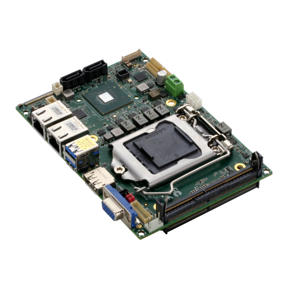
- Page 1 GENE-CML5 3.5” Subcompact Board User’s Manual 2 Last Updated: March 11, 2021...
- Page 2 Copyright Notice This document is copyrighted, 2021. All rights are reserved. The original manufacturer reserves the right to make improvements to the products described in this manual at any time without notice. No part of this manual may be reproduced, copied, translated, or transmitted in any form or by any means without the prior written permission of the original manufacturer.
- Page 3 Acknowledgement All other products’ name or trademarks are properties of their respective owners. Microsoft Windows is a registered trademark of Microsoft Corp. ⚫ Intel, Pentium, and Celeron are registered trademarks of Intel Corporation ⚫ Intel Core is a registered trademark of Intel Corporation ⚫...
- Page 4 Packing List Before setting up your product, please make sure the following items have been shipped: Item Quantity GENE-CML5 CPU Cooler (TH1CML5010) CPU Cooler Backplate (TH6CML5010) Screw Kit (9767ECD001) If any of these items are missing or damaged, please contact your distributor or sales representative immediately.
- Page 5 About this Document This User’s Manual contains all the essential information, such as detailed descriptions and explanations on the product’s hardware and software features (if any), its specifications, dimensions, jumper/connector settings/definitions, and driver installation instructions (if any), to facilitate users in setting up their product. Users may refer to the product page at AAEON.com for the latest version of this document.
- Page 6 Safety Precautions Please read the following safety instructions carefully. It is advised that you keep this manual for future references All cautions and warnings on the device should be noted. Make sure the power source matches the power rating of the device. Position the power cord so that people cannot step on it.
- Page 7 If any of the following situations arises, please the contact our service personnel: Damaged power cord or plug Liquid intrusion to the device iii. Exposure to moisture Device is not working as expected or in a manner as described in this manual The device is dropped or damaged Any obvious signs of damage displayed on the device...
- Page 8 FCC Statement This device complies with Part 15 FCC Rules. Operation is subject to the following two conditions: (1) this device may not cause harmful interference, and (2) this device must accept any interference received including interference that may cause undesired operation.
- Page 9 China RoHS Requirements (CN) 产品中有毒有害物质或元素名称及含量 AAEON Main Board/ Daughter Board/ Backplane 有毒有害物质或元素 部件名称 铅 汞 镉 六价铬 多溴联苯 多溴二苯醚 (Pb) (Hg) (Cd) (Cr(VI)) (PBB) (PBDE) 印刷电路板 ○ ○ ○ ○ ○ ○ 及其电子组件 外部信号 ○ ○ ○ ○ ○ ○ 连接器及线材...
- Page 10 China RoHS Requirement (EN) Poisonous or Hazardous Substances or Elements in Products AAEON Main Board/ Daughter Board/ Backplane Poisonous or Hazardous Substances or Elements Hexavalent Polybrominated Polybrominated Component Lead Mercury Cadmium Chromium Biphenyls Diphenyl Ethers (Pb) (Hg) (Cd) (Cr(VI)) (PBB) (PBDE) PCB &...
-
Page 11: Table Of Contents
Table of Contents Chapter 1 - Product Specifications..................1 Specifications ......................2 Chapter 2 – Hardware Information ..................5 Dimensions ....................... 6 Jumpers and Connectors ..................9 List of Jumpers ......................11 2.3.1 LVDS Operating VDD Selection (JP1) ............11 2.3.2 LVDS Backlight VCC Selection (JP1) ............ - Page 12 2.4.15 LVDS Port Inverter/ Backlight Connector (CN18) ........27 2.4.16 LAN (RJ-45) Port 2 (CN19) ................. 27 2.4.17 LAN (RJ-45) Port 2 (CN20) ................. 28 2.4.18 USB 3.2 Gen 2 Port 1/ Port 2 (Dual Port) (CN21) ........29 2.4.19 DP++ Port (CN22) ..................
- Page 13 3.4.8.2 Legacy Console Redirection Settings..........59 3.4.8.3 Out-of-Band Mgmt Console Redirection Settings..... 60 3.4.9 Power Management ..................62 3.4.10 Digital IO Port Configuration ..............63 Setup Submenu: Chipset ..................64 3.5.1 North Bridge ....................65 3.5.1.1 LVDS Panel Configuration ............... 66 3.5.2 PCH IO Configuration .................
-
Page 14: Chapter 1 - Product Specifications
Chapter 1 Chapter 1 - Product Specifications... -
Page 15: Specifications
Specifications System Form Factor 3.5" Subcompact Board Intel® 10th Generation Core™ i7/i5/i3/Pentium/Celeron SoC i7-10700TE (8C, 2.0 GHz, up to 4.4 GHz) i5-10500TE (6C, 2.3 GHz, up to 3.7 GHz) i3-10100TE (4C, 2.3 GHz, up to 3.6 GHz) G6400TE (2C, 3.2 GHz) G5900TE (2C, 3.0 GHz) CPU Frequency Up to 4.4GHz... - Page 16 System Certification CE/FCC Class A Display CRT/LCD Controller Chrontel CH7517A Video Output DP++ x 1 VGA x 1 LVDS x 1 Backlight Inverter supply Max 12V, 2A Ethernet Intel® i210/i211,10/100/1000Base, RJ45 x1 Intel® i219,10/100/1000Base, RJ45 x1 (Support vPro® only with i5/i7 + Q470/Q470E variant) Audio High Definition Audio Interface, Line-in/Line-out/MIC (Without Amplifier)
- Page 17 — TPM 2.0 Touch — Others — Chapter 1 – Product Specifications...
-
Page 18: Chapter 2 - Hardware Information
Chapter 2 Chapter 2 – Hardware Information... -
Page 19: Dimensions
Dimensions Chapter 2 – Hardware Information... - Page 20 Part No. GENE-CML5-FAN01 With Thermal Option ( Chapter 2 – Hardware Information...
- Page 21 Thermal Option Assembly Chapter 2 – Hardware Information...
-
Page 22: Jumpers And Connectors
Jumpers and Connectors Chapter 2 – Hardware Information... - Page 23 Chapter 2 – Hardware Information...
-
Page 24: List Of Jumpers
List of Jumpers Please refer to the table below for all of the board’s jumpers that you can configure for your application Label Function LVDS Operating VDD Selection & Backlight VCC Selection Auto Power Button Enable/Disable Selection LVDS Backlight (BKLT) Control Selection Clear CMOS 2.3.1 LVDS Operating VDD Selection (JP1) -
Page 25: Auto Power Button Enable/Disable Selection (Jp2)
2.3.3 Auto Power Button Enable/Disable Selection (JP2) 1 2 3 Disabled Enabled (Default) Note: When disabled, Power Button must be used to power on the system. 2.3.4 LVDS Backlight Control Selection (JP3) 1 2 3 VR Mode PWM Mode (Default) 2.3.5 Clear CMOS Jumper (JP5) Normal (Default) -
Page 26: List Of Connectors
List of Connectors Please refer to the table below for all of the board’s connectors that you can configure for your application Label Function COM Port 2 COM Port 1 External +5VSB Input External Power Input Audio I/O Port Digital IO Port SATA Port SATA Port CN10... -
Page 27: Com Port 1/ Port 2 (Cn1/Cn2)
Label Function CN25 BIOS Debug Port CN26 M.2 M-Key DIMM1 DDR4 SO-DIMM Slot DIMM2 DDR4 SO-DIMM Slot 2.4.1 COM Port 1/ Port 2 (CN1/CN2) Note: CN1 is COM Port 2; and CN2 is COM Port 1. RS-232 Pin Name Signal Type Signal Level Chapter 2 –... - Page 28 RS-485 Pin Name Signal Type Signal Level RS485_ D- RS485_D+ RS-422 Pin Name Signal Type Signal Level RS422_TX- RS422_TX+ RS422_RX+ RS422_RX- Note 1: COM Port RS-232/422/485 can be set by BIOS. Default is RS-232. Chapter 2 – Hardware Information...
-
Page 29: External +5Vsb Input (Cn3)
2.4.2 External +5VSB Input (CN3) Pin Name Signal Type Signal Level PS_ON# +V5A_SB_IN 2.4.3 External Power Input (CN5) Pin Name Signal Type Signal Level +VIN_EXT Chapter 2 – Hardware Information... -
Page 30: Audio I/O Port (Cn6)
2.4.4 Audio I/O Port (CN6) Pin Name Signal Type Signal Level MIC_L MIC_R GND_AUDIO LINE_L LINE_R GND_AUDIO LEFT_OUT GND_AUDIO RIGHT_OUT +5V_AUDIO Chapter 2 – Hardware Information... -
Page 31: Digital I/O Port (Cn7)
2.4.5 Digital I/O Port (CN7) Pin Name Signal Type Signal Level +V5S DIO0 DIO1 DIO2 DIO3 DIO4 DIO5 DIO6 DIO7 Note: DIO +V5S max driving current is 0.5A Chapter 2 – Hardware Information... -
Page 32: Sata Port (Cn8/Cn9)
2.4.6 SATA Port (CN8/CN9) Pin 1 Pin 7 Pin Name Signal Type Signal Level SATA_TX+ DIFF SATA_TX- DIFF SATA_RX- DIFF SATA_RX+ DIFF 2.4.7 +5V Output for SATA HDD (CN10) Pin Name Signal Type Signal Level Note: SATA HDD +V5S max driving current is 0.5A Chapter 2 –... -
Page 33: Battery Connector (Cn11)
2.4.8 Battery Connector (CN11) Pin Name Signal Type Signal level +3.3V 3.3V 2.4.9 USB 2.0 Port (CN12) Pin Name Signal Type Signal Level +V5A_USB_3 +V5A_USB_3 USBD5- DIFF USBD6- DIFF USBD5+ DIFF USBD6+ DIFF Chapter 2 – Hardware Information... -
Page 34: Usb 2.0 Port (Cn13)
2.4.10 USB 2.0 Port (CN13) Pin Name Signal Type Signal Level +V5A_USB_2 +V5A_USB_2 USBD3- DIFF USBD4- DIFF USBD3+ DIFF USBD4+ DIFF Chapter 2 – Hardware Information... -
Page 35: Fpc (Cn14)
2.4.11 FPC (CN14) Pin Name Signal Type Signal Level +V3P3S +3.3V +V3P3S +3.3V +V3P3S +3.3V SMB_DATA SMB_CLK BUF_PLT_RST# +V3P3A +3.3V PCIE_18_RXP DIFF PCIE_18_RXN DIFF PCIE_20_RXP DIFF PCIE_20_RXN DIFF PCIE_19_RXP DIFF PCIE_19_RXN DIFF Chapter 2 – Hardware Information... - Page 36 Pin Name Signal Type Signal Level PCIE_17_RXP DIFF PCIE_17_RXN DIFF PCIE_20_TXN DIFF PCIE_20_TXP DIFF PCIE_19_TXN DIFF PCIE_19_TXP DIFF PCIE_18_TXN DIFF PCIE_18_TXP DIFF CLK_PCIE_FPC_N DIFF CLK_PCIE_FPC_P DIFF PCIE_17_TXN DIFF PCIE_17_TXP DIFF +V12S +V12S +V12S +V12S +V12S Chapter 2 – Hardware Information...
-
Page 37: Cpu Fan (Cn15)
2.4.12 CPU Fan (CN15) Pin Name Signal Type Signal Level FAN_POWER +12V FAN_TAC FAN_CTL Note: FAN Connector FAN_POWER max driving current is 1A 2.4.13 Digital I/O Port (CN16) Pin Name Signal Type Signal Level EXT_PWRBTN# FP_HDLED- Chapter 2 – Hardware Information... -
Page 38: Lvds Port (Cn17)
Pin Name Signal Type Signal Level FP_HDLED+ FP_SPKR- +V5S PWRLED+ HWRST# 2.4.14 LVDS Port (CN17) Note: LVDS Operating VDD can be set by JP1, reference Ch 2.3.1 for details Pin Name Signal Type Signal Level LVDS_BKLTEN +VDD_LVDS LVDSA_CLK# DIFF +VDD_LVDS LVDSA_DATA0# DIFF LVDSA_DATA1#... - Page 39 Pin Name Signal Type Signal Level LVDS_DDC_DATA LVDSB_DATA0# DIFF LVDSB_DATA1# DIFF LVDSB_DATA2# DIFF LVDSB_DATA3# DIFF +VDD_LVDS LVDSB_CLK# DIFF LVDS_BKLCTL LVDSA_CLK DIFF LVDSA_DATA0 DIFF LVDSA_DATA1 DIFF LVDSA_DATA2 DIFF LVDSA_DATA3 DIFF LVDS_DDC_CLK LVDSB_DATA0 DIFF LVDSB_DATA1 DIFF LVDSB_DATA2 DIFF LVDSB_DATA3 DIFF LVDSB_CLK DIFF Note: LVDS Connector +VDD_LVDS max driving current is 0.5A Chapter 2 –...
-
Page 40: Lvds Port Inverter/ Backlight Connector (Cn18)
2.4.15 LVDS Port Inverter/ Backlight Connector (CN18) Pin Name Signal Type Signal level +VCC_LVDS_BKLT +VCC_LVDS_BKLT L_BKLTNESS LVDS_BKLTEN Note 1: LVDS Backlight VCC can be by JP1. (See Ch 2.3.2) Note 2: Backlight Connector +VCC_LVDS_BKLT max driving current is 1.5A 2.4.16 LAN (RJ-45) Port 2 (CN19) Pin Name Signal Type... -
Page 41: Lan (Rj-45) Port 2 (Cn20)
Pin Name Signal Type Signal level LAN2_MDI2- DIFF LAN2_MDI1- DIFF LAN2_MDI3+ DIFF LAN2_MDI3- DIFF 2.4.17 LAN (RJ-45) Port 2 (CN20) ACT/LINK SPEED Pin Name Signal Type Signal level LAN1_MDI0+ DIFF LAN1_MDI0- DIFF LAN1_MDI1+ DIFF LAN1_MDI2+ DIFF LAN1_MDI2- DIFF LAN1_MDI1- DIFF LAN1_MDI3+ DIFF LAN1_MDI3-... -
Page 42: Usb 3.2 Gen 2 Port 1/ Port 2 (Dual Port) (Cn21)
2.4.18 USB 3.2 Gen 2 Port 1/ Port 2 (Dual Port) (CN21) Pin Name Signal Type Signal Level +V5A_USB_1 USBD2- DIFF USBD2+ DIFF USB3_RX2_CON_N DIFF USB3_RX2_CON_P DIFF USB3_TX2_CON_N DIFF USB3_TX2_CON_P DIFF +V5A_USB_0 USBD1- DIFF USBD1+ DIFF USB3_RX1_CON_N DIFF USB3_RX1_CON_P DIFF USB3_TX1_CON_N DIFF USB3_TX1_CON_P... -
Page 43: Dp++ Port (Cn22)
2.4.19 DP++ Port (CN22) Pin Name Signal Type Signal Level DDI1_TX0_DP DIFF DDI1_TX0_DN DIFF DDI1_TX1_DP DIFF DDI1_TX1_DN DIFF DDI1_TX2_DP DIFF DDI1_TX2_DN DIFF DDI1_TX3_DP DIFF DDI1_TX3_DN DIFF DDI1_AUX_EN DDI1_DP_CTRLCLK_AUX_DP DIFF DDI1_DP_CTRLDATA_AUX_DN DIFF DDI1_DP_HPD DDI1_DP_HPD +V3P3S Chapter 2 – Hardware Information... -
Page 44: Vga Port (Cn23)
2.4.20 VGA Port (CN23) Pin Name Signal Type Signal Level VGA_RED_CON VGA_GREEN_CON VGA_BLUE_CON RED_GND_RTN GREEN_GND_RTN BLUE_GND_RTN VGA_DDCDAT_CON VGA_HSYNC_CON VGA_VSYNC_CON VGA_DDCCLK_CON Chapter 2 – Hardware Information... -
Page 45: Lpc Port (Cn24)
2.4.21 LPC Port (CN24) Pin Name Signal Type Signal Level LPC_AD0 LPC_AD1 LPC_AD2 LPC_AD3 +V3P3S +3.3V LPC_FRAME# BUF_PLT_RST# CLK_LPCC_25M I2C0_SDA I2C0_SCL INT_SERIRQ Chapter 2 – Hardware Information... -
Page 46: Bios Debug Port (Cn25)
2.4.22 BIOS Debug Port (CN25) Pin Name Signal Type Signal Level SPI_SO_F SPI_CLK_F +V3P3A_SPI +3.3V SPI_SI_F SPI_CE0#_F 2.4.23 M.2 M-Key 2280 (CN26) Pin Name Signal Type Signal Level +V3P3S +3.3V +V3P3S +3.3V PCIE_8_RXN DIFF CARD_PWR_OFF_R PCIE_8_RXP DIFF Chapter 2 – Hardware Information... - Page 47 Pin Name Signal Type Signal Level SSD_LED# PCIE_8_TXN_C DIFF +V3P3S +3.3V PCIE_8_TXP_C DIFF +V3P3S +3.3V +V3P3S +3.3V PCIE_7_RXN DIFF +V3P3S +3.3V PCIE_7_RXP DIFF PCIE_7_TXN_C DIFF PCIE_7_TXP_C PCIE_6_RXN DIFF PCIE_6_RXP DIFF Chapter 2 – Hardware Information...
- Page 48 Pin Name Signal Type Signal Level PCIE_6_TXN_C DIFF PCIE_6_TXP_C DIFF SATA_DEVSLP0 SMB_CLK_KMB M2M_A_RXP DIFF M2M_A_RXN DIFF M2M_A_TXN_C DIFF M2M_A_TXP_C DIFF BUF_PLT_RST# M2M_CLKREQ# CLK_PCIE_M2M_N_R PCIE_WAKE# CLK_PCIE_M2M_P_R Chapter 2 – Hardware Information...
-
Page 49: Ddr4 So-Dimm Slot (Dimm1/ Dimm2)
Pin Name Signal Type Signal Level SUS_CLK_M2M PEDET_R +V3P3S +3.3V +V3P3S +3.3V +V3P3S +3.3V 2.4.24 DDR4 SO-DIMM Slot (DIMM1/ DIMM2) Standard Specifications Chapter 2 – Hardware Information... -
Page 50: Block Diagram
Block Diagram Chapter 2 – Hardware Information... -
Page 51: Chapter 3 - Ami Bios Setup
Chapter 3 Chapter 3 - AMI BIOS Setup... -
Page 52: System Test And Initialization
System Test and Initialization The GENE-CML5 board uses certain routines to perform testing and initialization during the boot up sequence. If an error, fatal or non-fatal, is encountered, the module will output a few short beeps or display an error message. The module can usually continue the boot up sequence with non-fatal errors. -
Page 53: Ami Bios Setup
AMI BIOS Setup The AMI BIOS ROM has a pre-installed Setup program that allows users to modify basic system configurations, which is stored in the battery-backed CMOS RAM and BIOS NVRAM so that the information is retained when the power is turned off. To enter BIOS Setup, press <Del>... -
Page 54: Setup Submenu: Main
Setup Submenu: Main Chapter 3 – AMI BIOS Setup... -
Page 55: Setup Submenu: Advanced
Setup Submenu: Advanced Chapter 3 – AMI BIOS Setup... -
Page 56: Trusted Computing
3.4.1 Trusted Computing Options Summary Security Device Support Disable Enable Optimal Default, Failsafe Default Enables or Disables BIOS support for security device. O.S. will not show Security Device. TCG EFI protocol and INT1A interface will not be available. SHA-1 PCR Bank Disabled Optimal Default, Failsafe Default Enabled... - Page 57 Options Summary Platform Hierarchy Disabled Enabled Optimal Default, Failsafe Default Enable or disable Platform Hierarchy Storage Hierarchy Disabled Enabled Optimal Default, Failsafe Default Enable or Disable Storage Hierarchy Endorsement Hierarchy Disabled Enabled Optimal Default, Failsafe Default Enable or Disable Endorsement Hierarchy TPM2.0 UEFI Spec Version TCG_1_2 TCG_2...
-
Page 58: Cpu Configuration
3.4.2 CPU Configuration Options Summary Hyper-Threading Disabled Enabled Optimal Default, Failsafe Default Enabled or Disabled Hyper-Threading Technology Active Processor Cores Optimal Default, Failsafe Default Number of cores to enable in each processor package. Intel (VMX) Virtualization Disabled Technology Enabled Optimal Default, Failsafe Default When enabled, a VMM can utilize the additional hardware capabilities provided by Vanderpool Technology. - Page 59 Options Summary Turbo Mode Disabled Enabled Optimal Default, Failsafe Default Enable/Disable processor Turbo Mode (requires Intel Speed Step or Intel Speed Shift to be available and enabled). Chapter 3 – AMI BIOS Setup...
-
Page 60: Sata Configuration
3.4.3 SATA Configuration Options Summary SATA Controller(s) Enabled Optimal Default, Failsafe Default Enable/Disable SATA Device. SATA Mode Selection AHCI Optimal Default, Failsafe Default Intel RST Premium With Intel Optane System Acceleration Determines how SATA controller(s) operate M.2(CN26) Disabled Enabled Optimal Default, Failsafe Default Enable or Disable SATA Port Port 2 Disabled... - Page 61 Options Summary Hot Plug Disabled Optimal Default, Failsafe Default Enabled Designates this port as Hot Pluggable Port 3 Disabled Enabled Optimal Default, Failsafe Default Enable or Disable SATA Port Hot Plug Disabled Optimal Default, Failsafe Default Enabled Designates this port as Hot Pluggable Chapter 3 –...
-
Page 62: Hardware Monitor
3.4.4 Hardware Monitor Options Summary Smart Fan Disabled Enabled Optimal Default, Failsafe Default Enables or Disables Smart Fan. Chapter 3 – AMI BIOS Setup... -
Page 63: Smart Fan Mode Configuration
3.4.4.1 Smart Fan Mode Configuration Options Summary FAN1 Output Output PWM mode Mode (open drain) Linear Fan Application Output PWM mode Optimal Default, Failsafe Default (push pull) Fan 1 Smart Fan Manual Duty Mode Control Auto Duty-Cycle Mode Optimal Default, Failsafe Default Smart Fan Mode Select Temperature CPU(PECI) Temperature... -
Page 64: Sio Configuration
3.4.5 SIO Configuration Chapter 3 – AMI BIOS Setup... -
Page 65: Serial Port 1 Configuration
3.4.5.1 Serial Port 1 Configuration Options Summary Use This Device Disable Enable Optimal Default, Failsafe Default Enable or Disable this Logical Device. Possible: Use Automatic Optimal Default, Failsafe Default Settings IO=3F8h; IRQ=4 IO=2F8h; IRQ=3 Allows user to change Device's Resource settings. New settings will be reflected on This Setup Page after System restarts. -
Page 66: Serial Port 2 Configuration
3.4.5.2 Serial Port 2 Configuration Options Summary Use This Device Disable Enable Optimal Default, Failsafe Default Enable or Disable this Logical Device. Possible: Use Automatic Optimal Default, Failsafe Default Settings IO=2F8h; IRQ=3 IO=3F8h; IRQ=4 Allows user to change Device's Resource settings. New settings will be reflected on This Setup Page after System restarts. -
Page 67: Amt Configuration
3.4.6 AMT Configuration Options Summary AMT BIOS Features Disable Enable Optimal Default, Failsafe Default When disabled AMT BIOS Features are no longer supported and user is no longer able to access MEBx Setup. Note: This option does not disable Manageability Features in FW Chapter 3 –... -
Page 68: Firmware Update Configuration
3.4.7 Firmware Update Configuration Options Summary Me FW Image Re-Flash Disabled Optimal Default, Failsafe Default Enabled Enable/Disable Me FW Image Re-Flash function. FW Update Disabled Enabled Optimal Default, Failsafe Default Enable/Disable ME FW Update function. Chapter 3 – AMI BIOS Setup... -
Page 69: Serial Port Console Redirection
3.4.8 Serial Port Console Redirection Options Summary Console Redirection Disabled Optimal Default, Failsafe Default Enabled Console Redirection Enable or Disable. Console Redirection EMS Disabled Optimal Default, Failsafe Default Enabled Console Redirection Enable or Disable. Chapter 3 – AMI BIOS Setup... -
Page 70: Com0 Console Redirection Settings
3.4.8.1 COM0 Console Redirection Settings Options Summary Terminal Type VT100 VT100+ VT-UTF8 ANSI Optimal Default, Failsafe Default Emulation: ANSI: Extended ASCII char set. VT100: ASCII char set. VT100+: Extends VT100 to support color, function keys, etc. VT-UTF8: Uses UTF8 encoding to map Unicode chars onto 1 or more bytes. - Page 71 Options Summary Even Mark Space A parity bit can be sent with the data bits to detect some transmission errors. Even: parity bit is 0 if the num of 1's in the data bits is even. Odd: parity bit is 0 if num of 1's in the data bits is odd.
-
Page 72: Legacy Console Redirection Settings
3.4.8.2 Legacy Console Redirection Settings Options Summary Redirection Console COM COM0 Optimal Default, Failsafe Default Port Console Redirection Enable or Disable. Resolution 80x24 Optimal Default, Failsafe Default 80x25 On Legacy OS, the Number of Rows and Columns supported redirection Redirect After POST Always Enable Optimal Default, Failsafe Default BootLoader... -
Page 73: Out-Of-Band Mgmt Console Redirection Settings
3.4.8.3 Out-of-Band Mgmt Console Redirection Settings Options Summary Terminal Type EMS VT100 VT100+ VT-UTF8 Optimal Default, Failsafe Default ANSI VT-UTF8 is the preferred terminal type for out-of-band management. The next best choice is VT100+ and then VT100. See above, in Console Redirection Settings page, for more Help with Terminal Type/Emulation. - Page 74 Options Summary Flow control can prevent data loss from buffer overflow. When sending data, if the receiving buffers are full, a 'stop' signal can be sent to stop the data flow. Once the buffers are empty, a 'start' signal can be sent to re-start the flow. Hardware flow control uses two wires to send start/stop signals.
-
Page 75: Power Management
3.4.9 Power Management Options Summary Power Mode ATX Type Optimal Default, Failsafe Default AT Type Select system power mode State After G3 Always On Always Off Last State Optimal Default, Failsafe Default Specify what state to go to when power is re-applied after a power failure (G3 state). -
Page 76: Digital Io Port Configuration
3.4.10 Digital IO Port Configuration Options Summary DIO Port* Output Input Set DIO as Input or Output Output Level High Optimal Default, Failsafe Default Set output level when DIO pin is output Chapter 3 – AMI BIOS Setup... -
Page 77: Setup Submenu: Chipset
Setup Submenu: Chipset Chapter 3 – AMI BIOS Setup... -
Page 78: North Bridge
3.5.1 North Bridge Chapter 3 – AMI BIOS Setup... -
Page 79: Lvds Panel Configuration
3.5.1.1 LVDS Panel Configuration Options Summary LVDS Disabled Enabled Optimal Default, Failsafe Default Enable/Disabled this panel. LVDS Panel Type 640x480,18bit,60Hz 800x480,18bit,60Hz 800x600,18bit,60Hz 1024x600,18bit,60Hz 1024x768,18bit,60Hz 1024x768,24bit,60Hz Optimal Default, Failsafe Default 1280x768,24bit,60Hz 1280x1024,48bit,60Hz 1366x768,24bit,60Hz 1440x900,48bit,60Hz 1600x1200,48bit,60Hz 1920x1080,48bit,60Hz 1920x1200,48bit,60Hz Select LCD panel used by Internal Graphics Device by selecting the appropriate setup item. - Page 80 Options Summary Color Depth 18-bit Optimal Default, Failsafe Default 24-bit 36-bit 48-bit Select panel type Backlight Type Normal Optimal Default, Failsafe Default Inverted Select backlight control signal type Backlight Level Optimal Default, Failsafe Default 100% Select backlight control level Backlight PWM Freq 100Hz 200Hz 220Hz...
-
Page 81: Pch Io Configuration
3.5.2 PCH IO Configuration Options Summary HD Audio Disabled Enabled Optimal Default, Failsafe Default Control Detection of the HD-Audio device. Disabled = HDA will be unconditionally disabled Enabled = HDA will be unconditionally enabled. PCH Lan Controller Disabled Enabled Optimal Default, Failsafe Default Enable/Disable onboard NIC Chapter 3 –... -
Page 82: Setup Submenu: Security
Setup Submenu: Security Change User/Administrator Password You can set an Administrator Password or User Password. An Administrator Password must be set before you can set a User Password. The password will be required during boot up, or when the user enters the Setup utility. A User Password does not provide access to many of the features in the Setup utility. -
Page 83: Secure Boot
3.6.1 Secure Boot Options Summary Secure Boot Disabled Optimal Default, Failsafe Default Enabled Secure Boot feature is Active if Secure Boot is Enabled, Platform Key (PK) is enrolled and the System is in User mode. The mode change requires platform reset Secure Boot Mode Custom... -
Page 84: Key Management
3.6.1.1 Key Management Options Summary Factory Key Provision Disabled Optimal Default, Failsafe Default Enabled Secure Boot feature is Active if Secure Boot is Enabled, Platform Key (PK) is enrolled and the System is in User mode. The mode change requires platform reset Restore Factory Keys Force System to User Mode. - Page 85 Options Summary Remove 'UEFI CA' from DB Device Guard ready system must not list 'Microsoft UEFI CA' Certificate in Authorized Signature database (db) Restore DB defaults Restore DB variable to factory defaults Platform Key (PK) Details Export Update Delete Key Exchange Keys Details Export Update...
-
Page 86: Setup Submenu: Boot
Setup Submenu: Boot Options Summary Quiet Boot Disabled Enabled Optimal Default, Failsafe Default Enable or Disable showing boot logo. LAN UEFI Pxe Driver Disabled Optimal Default, Failsafe Default Enabled Enabled/Disable LAN UEFI PXE Driver Chapter 3 – AMI BIOS Setup... -
Page 87: Bbs Priorities
3.7.1 BBS Priorities Chapter 3 – AMI BIOS Setup... -
Page 88: Setup Submenu: Save & Exit
Setup Submenu: Save & Exit Chapter 3 – AMI BIOS Setup... -
Page 89: Chapter 4 - Driver Installation
Chapter 4 Chapter 4 – Driver Installation... -
Page 90: Driver Download/Installation
Driver Download/Installation Drivers for the GENE-CML5 can be downloaded from the product page on the AAEON website by following this link: https://www.aaeon.com/en/p/subcompact-boards-gene-cml5 Download the driver(s) you need and follow the steps below to install them. Step 1 – Install Chipset Drivers Open the Step 1 –... - Page 91 Step 4 – Install Audio Driver Open the Step 4 – Audio folder Run the Win10_R281.exe file in the folder Follow the instructions Drivers will be installed automatically Step 5 – Install Serial IO Drivers Open the Step 5 – SerialIO folder Run the SetupSerialIO.exe file in the folder Follow the instructions Drivers will be installed automatically...
-
Page 92: Appendix A - I/O Information
Appendix A Appendix A - I/O Information... -
Page 93: I/O Address Map
I/O Address Map Appendix A – I/O Information... - Page 94 Appendix A – I/O Information...
-
Page 95: A.2 Memory Address Map
A.2 Memory Address Map Appendix A – I/O Information... -
Page 96: A.3 Irq Mapping Chart
A.3 IRQ Mapping Chart Appendix A – I/O Information... - Page 97 Appendix A – I/O Information...
- Page 98 Appendix A – I/O Information...
-
Page 99: Appendix B - Mating Connectors And Cables
Appendix B Appendix B – Mating Connectors and Cables... -
Page 100: Mating Connectors And Cables
Mating Connectors and Cables Mating Connector Connector Available Function Cable P/N Label Cable Vendor Model no COM Port 710-H73-095 Serial Port PINREX 1701090122 Connector Cable COM Port 710-H73-095 Serial Port PINREX 1701090122 Connector Cable 753-71-03TW PINREX ATX Cable 170220020B Connector Audio 712-71-10TW PINREX... -
Page 101: Appendix C - Digital I/O Ports
Appendix C Appendix C – Digital I/O Ports... -
Page 102: Digital I/O Register
Digital I/O Register Appendix C – Digital I/O Ports... - Page 103 Appendix C – Digital I/O Ports...
-
Page 104: Digital I/O Sample Code (4 In 4 Out, 2 Low 2 High)
Digital I/O Sample Code (4 in 4 out, 2 low 2 high) Outportb(0x2E,0x87); //enter configuration Outportb(0x2E,0x87); Outportb(0x2E,0x07); //set LDN Outportb(0x2F,0x06); Outportb(0x2E,0x88); //GPIO set 8x Output enable register Outportb(0x2F,0xF0); Outportb(0x2E,0x89); //GPIO 8x output data register Outportb(0x2F,0x30); Outportb(0x2E,0xAA); //exit configuration Appendix C – Digital I/O Ports...
Need help?
Do you have a question about the AAEON GENE-CML5 and is the answer not in the manual?
Questions and answers