
Related Manuals for artisan VME-SIO4A


Summary of Contents for artisan VME-SIO4A
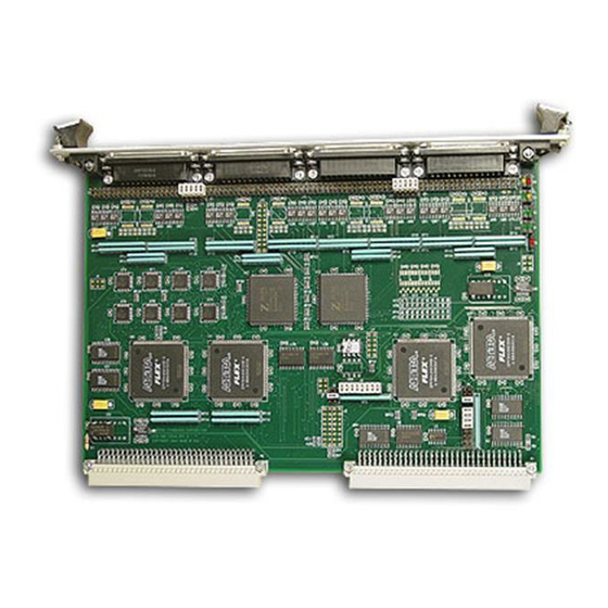
- Page 1 sales@artisantg.com artisantg.com (217) 352-9330 | Visit our website - Click HERE...
- Page 2 VME-SIO4A User Manual Manual Revision: B General Standards Corporation 8302A Whitesburg Drive Huntsville, AL 35802 Phone: (256) 880-8787 Fax: (256) 880-8788 URL : http://www.generalstandards.com E-mail techsupport@generalstandards.com Revision B User Manual for the VME-SIO4: Board Revision: A General Standards Corporation 8302A Whitesburg Drive Huntsville, AL 3580, Phone: (256) 880-8787...
- Page 3 PREFACE Copyright © 1997 General Standards Corp. Additional copies of this manual or other General Standards Corporation literature may be obtained from: General Standards Corporation 8302A Whitesburg Drive Huntsville, Alabama 35802 Telephone: (256) 880-8787 Fax: (256) 880-8788 Company URL: www.generalstandards.com The information in this document is subject to change without notice.
- Page 4 Related Publications The following manuals and specifications provide the necessary information for in-depth understanding of the VMEbus and specialized parts used on this board. EIA Standard for the RS-422-A Interface (EIA order number EIA-RS-422A) VMEbus Specification Manual (also known as IEC 821 BUS and IEEE P10114/D1/2), for information submit request to: VITA10229 North Scottsdale Road, Suite B Scottsdale, AZ 85253...
- Page 5 VME-SIO4 Documentation History 1) The Vme-SIO4 documentation was updated March 1997. 2) The manual was reformatted, for conformity of text, and the table of contents was corrected. 3) The jumper field drawings in Chapter 4 were redrawn and double checked. 4) April 27, 1997: Chapter 3, page 3, Section 3.1.2.1, D6 &...
-
Page 6: Table Of Contents
TABLE OF CONTENTS CHAPTER 1: INTRODUCTION..........................8 INTRODUCTION ............................8 FUNCTIONAL DESCRIPTION .........................8 BOARD IDENTIFICATION........................8 BOARD CONTROL REGISTER......................10 BOARD STATUS REGISTER .........................10 SYNC WORD SELECTION ........................10 DATA RECEPTION ..........................10 DATA TRANSMIT ...........................10 LOOP-BACK TESTING ...........................10 ERROR DETECTION..........................10 1.10 INTERRUPTS ............................10 1.11 DIAGNOSTIC LED DISPLAYS.......................11 1.12 CABLE INTERFACE CONNECTIONS....................11 CHAPTER 2: THEORY OF OPERATION......................12... - Page 7 3.1.6.5.2 High: (Offset Address: 0x12) .........................25 3.1.6.6 Secondary Reserved Register (Address: 00101) ................26 3.1.6.6.1 Low: (Offset Address: 0x14)........................26 3.1.6.6.2 High: (Offset Address: 0x16) .........................26 3.1.6.7 Test Mode Data Register (Address: 00110)..................26 3.1.6.7.1 Low: (Offset Address: 0x18)........................26 3.1.6.7.2 High: (Offset Address: 0x1A) ........................26 3.1.6.8 Test Mode Control Register (Address: 00111) .................26 3.1.6.8.1...
- Page 8 3.1.6.25 Transmit Mode Register (Address: 11001)..................37 3.1.6.25.1 Low: (Offset Address: 0x64)........................37 3.1.6.25.2 High: (Offset Address: 0x66) ........................37 3.1.6.26 Transmit Command/Status Register (Address: 11010)..............38 3.1.6.26.1 Low: (Offset Address: 0x68)........................38 3.1.6.26.2 High: (Offset Address: 0x6A) ........................38 3.1.6.27 Transmit Interrupt Control Register (Address: 11011) ..............39 3.1.6.27.1 Low: (Offset Address: 0x6C) ........................39 3.1.6.27.2 High: (Offset Address: 0x6E)........................39 3.1.6.28 Transmit Sync Register (Address: 11100) ..................39...
-
Page 9: Chapter 1: Introduction
CHAPTER 1: INTRODUCTION INTRODUCTION The VME-SI04 interface card is capable of transmitting and receiving serial data, generating interrupts, and providing loop-back testing. This card provides the following specific functionality: a. VMEbus Interface: (1) 6U card (single slot. IEEE/ANSI-1014 compliant; A16/D16 support or better. (2) VMEbus interrupter functionality. - Page 10 Figure 1.1-1: Functional Block Diagram Revision B User Manual for the VME-SIO4: Board Revision: A General Standards Corporation 8302A Whitesburg Drive Huntsville, AL 3580, Phone: (256) 880-8787...
-
Page 11: Board Control Register
BOARD CONTROL REGISTER The board control register will provide configuration of the board, including the self-test modes. BOARD STATUS REGISTER The board status register will provide status with regard to receive FIFO status and transmit FIFO status. SYNC WORD SELECTION The sync word selection is used to provide an interrupt upon the reception of a particular character. -
Page 12: Diagnostic Led Displays
Interrupt status bits are cleared by writing a 1 to the respective bit in the interrupt status register. A second interrupt from that bit will not occur until after that status bit has been cleared. 1.11 DIAGNOSTIC LED DISPLAYS LEDs provide for indication of the following conditions: a. -
Page 13: Chapter 2: Theory Of Operation
CHAPTER 2: THEORY OF OPERATION THE BOARD INTERFACE This board operates as an interface for two Zilog Z16C30s, giving it Quad Channel capabilities. The Zilogs are mapped into the base address of this board and all reads and writes are PIOs. This board does not offer DMA across the VMEbus. -
Page 14: Cable
run at full speed without interfering with each other. The VME can read and write the Zilog during DMA cycles. However, it must wait until the end of the current DMA access when the DMA finishes its current access, then the VME will be allowed onto the Zilog bus. -
Page 15: Chapter 3: Programming
CHAPTER 3: PROGRAMMING REGISTER MAP The register address map for the VME-SI04 is shown below.. This board contains registers for Board Control, I/O Control, FIFO Control, Interrupt Control and Serial Controller. Table 3.0-1 VME-SI04 Register Address Map Address Offset Size* Access** Register Name Board... -
Page 16: Register Bit Maps
REGISTER BIT MAPS All Reserved bits should be set to 0 for future compatibility. Also, the value read from a reserved bit will be indeterminate. 3.1.1 BOARD CONTROL/STATUS REGISTERS: 3.1.1.1 Board ID Register: D0..D16 Reads back hex CEAC 3.1.1.2 Device Type Register: D0..D16 Reads back hex F4E4 3.1.1.3 Board Control Register: Board Reset L (pulsed) -
Page 17: Channel 0 Fifo: (Same Format For Channels 1
En Drive Lower Cable H 1 will enable this board to drive the lower cable. 0 will disable this board from driving the lower cable. En Drive Upper Cable H 1 will enable this board to drive the upper cable. 0 will disable this board from driving the upper cable. -
Page 18: Interrupt Control/Status Registers
3.1.5 INTERRUPT CONTROL/STATUS REGISTERS: 3.1.5.1 Interrupt Control Register Enable Channel 0 Sync Detected 1 will enable this board to generate an interrupt when a sync word is detected. 0 will disable this board from generating an interrupt when a sync word is detected. -
Page 19: Interrupt Status Register (Dual Purpose Bits): (Icr - Interrupt Control Register)
1 will enable this board to generate an interrupt when the Rx FIFO is not empty. 0 will disable this board from generating an Interrupt when the Rx FIFO is not empty. Enable Channel 2 Rx FIFO Almost Full Interrupt 1 will enable this board to generate an interrupt when the Rx FIFO is almost full. - Page 20 0 indicates an interrupt has not occurred. If this interrupt is not enabled: 0 indicates the current status of this interrupt source. 1 being the source of the interrupt is present. 0 being the source of the interrupt is not present. Channel 2 Tx FIFO Empty Interrupt If this interrupt is enabled:...
- Page 21 If this interrupt is enabled: 1 indicates an interrupt has occurred. 0 indicates an interrupt has not occurred. If this interrupt is not enabled: 0 indicates the current status of this interrupt source. 1 being the source of the interrupt is present. 0 being the source of the interrupt is not present.
-
Page 22: 3.1.5.3 Interrupt Vector Register
3.1.5.3 Interrupt Vector Register This is a hardware modifiable Interrupt Vector Register, to indicate the source of the interrupt, encoding is as follows D0 being the LSB: D0..D2 Hardware Encoded Enable Channel 0 Sync Detected Enable Channel 0 Tx FIFO Empty Interrupt Enable Channel 1 Sync Detected Enable Channel 1 Tx FIFO Empty Interrupt Enable Channel 2 Sync Detected... -
Page 23: High Wo: (Offset Address: 0X02)
3.1.6.1.2 High WO: (Offset Address: 0x02) Mode Control D0 WO 0 Normal Operation 1 Auto Echo 0 External Local Loop-back 1 Internal Local Loop-back D1 WO 0 Normal Operation 0 Auto Echo 1 External Local Loop-back 1 Internal Local Loop-back D2 WO Channel Reset Channel Command WO... -
Page 24: Low: (Offset Address: 0X04)
3.1.6.2.1 Low: (Offset Address: 0x04) Receiver Mode D3 RW D2 RW D1 RW D0 RW Bit Map Asynchronous External Synchronous Isochronous Asynchronous with CV Monosync Bisync HDLC Transparent Bisync NBIP 802.3 Reserved Reserved Reserved Reserved Reserved Reserved Rx Submode D7 RW D6 RW D5 RW D4 RW... -
Page 25: Channel Command/Status Register (Address: 00010)
D7 RW D6 RW D5 RW D4 RW 3.1.6.3 C : 00010) HANNEL OMMAND TATUS EGISTER DDRESS 3.1.6.3.1 Low: (Offset Address: 0x08) D5 RW Reserved Loop Sending D6 RO D7 RO On Loop HDLC Tx Last Character Length D4 RW D3 RW D2 RW Bit Map... -
Page 26: Channel Control Register (Address: 00011)
3.1.6.4 C : 00011) HANNEL ONTROL EGISTER DDRESS 3.1.6.4.1 Low: (Offset Address: 0x0C) Rx Status Block Transfer D7 RW D6 RW Bit Map No Status Block One Word Status Block Two Word Status Block Reserved D5 RW Wait for Rx DMA Trigger D0..4 RW Reserved 3.1.6.4.2 High: Address: 00011 Tx Status Block Transfer... -
Page 27: Secondary Reserved Register (Address: 00101)
D0..D7 RW Reserved 3.1.6.6 S : 00101) ECONDARY ESERVED EGISTER DDRESS 3.1.6.6.1 Low: (Offset Address: 0x14) D0..D7 RW Reserved 3.1.6.6.2 High: (Offset Address: 0x16) D0..D7 RW Reserved 3.1.6.7 T : 00110) EGISTER DDRESS 3.1.6.7.1 Low: (Offset Address: 0x18) D0..D7 RW Test Data 0 . .7 3.1.6.7.2 High: (Offset Address: 0x1A) D0..D7 RW Test Data 0 . -
Page 28: High: (Offset Address: 0X1E)
Reserved 4044H 4044H 4044H 4044H 4044H 4044H 4044H 4044H D5..D7 RW Reserved 3.1.6.8.2 High: (Offset Address: 0x1E) D0..D7 RW Reserved 3.1.6.9 C : 01000) LOCK ONTROL EGISTER DDRESS 3.1.6.9.1 Low: (Offset Address: 0x20) Receive Clock Source D2 RW D1 RW D0 RW Bit Map Disabled... -
Page 29: High: (Offset Address: 0X22)
DPLL Clock Source D7 RW D6 RW Bit Map BRG0 Output BRG1 Output /RxC Pin /TxC Pin 3.1.6.9.2 High: (Offset Address: 0x22) BRG0 Clock Source D1 RW D0 RW Bit Map CTR0 Output CTR1 Output /RxC Pin /TxC Pin BRG1 Clock Source D3 RW D2 RW Bit Map... -
Page 30: High: (Offset Address: 0X26)
D3 RW D2 RW Bit Map 3 - State Output Rx Acknowledge Input Output 0 Output 1 D5 RW BRG1 Enable D4 RW BRG1 Single Cycle/Continuous Tx ACK Pin Control D7 RW D6 RW Bit Map 3 - State Output Tx Acknowledge Input Output 0 Output 1... -
Page 31: Interrupt Vector Register (Address: 01010)
3.1.6.11 I : 01010) NTERRUPT ECTOR EGISTER DDRESS 3.1.6.11.1 Low: (Offset Address: 0x28) D7..D0 RW IV 0..7 3.1.6.11.2 High: (Offset Address: 0x2A) D0 RO IV 0 Modified Vector D3 RO D2 RO D1 RO Bit Map None Device Status I/O Status Transmit Data Transmit Status Receive Data... -
Page 32: High: (Offset Address: 0X2E)
D7 RW D6 RW Bit Map Tx Data Output 3-State Output Output 0 Output 1 3.1.6.12.2 High: (Offset Address: 0x2E) RxREQ Pin Control D1 RW D0 RW Bit Map 3-State Output Rx Request Output Output 0 Output 1 TxREQ Pin Control D3 RW D2 RW Bit Map... -
Page 33: High: (Offset Address: 0X32)
Null Command Null Command Reset IE Set IE 3.1.6.13.2 High: (Offset Address: 0x32) D0 RW Reserved VIS Level D3 RW D2 RW D1 RW Bit Map I/O Status and Above Transmit Data and Above Transmit Status and Above Receive Data and Above Receive Status Only None D7 RW MIE... -
Page 34: Misc. Interrupt Status Register (Address: 01110)
D4 RW Receive Data IUS D5 RW Receive Status IUS IUS Command D7 WO D6 WO Bit Map Null Command Null Command Reset IUS Set IUS 3.1.6.15 M : 01110) NTERRUPT TATUS EGISTER DDRESS 3.1.6.15.1 Low: (Offset Address: 0x38) D0 RW BRG0 ZC Latched/Unlatch D1 RW BRG1 ZC Latched/Unlatch D2 RW DPLL SYNC Latched/Unlatch D3 RW RCC Overflow Latched/Unlatch... -
Page 35: Tx/Rx Data Register (Address: 1X000)
D4 RW TxC Interrupts D5 RW TxC Interrupts D6 RW RxC Interrupts D7 RW RxC Interrupts 3.1.6.17 T 000) EGISTER DDRESS 3.1.6.17.1 Low: (Offset Address: 0x40) D0..7 RW - Tx/Rx Data 0..7 3.1.6.17.2 High: (Offset Address: 0x42) D0..7 RW - Tx/Rx Data 8..15 3.1.6.18 R : 10001) ECEIVER... -
Page 36: Receive Command Status Register (Address: 10010)
D2 RW Rx CRC Preset Value Rx CRC Polynomial D4 RW D3 RW Bit Map CRC-CCITT CRC-16 CRC-32 Reserved Rx Data Decoding D7 RW D6 RW D5 RW Bit Map NRZB NRZI-Mark NRZI-Space Biphase-Mark Biphase-Space Biphase-Level Diff. Biphase-Level 3.1.6.19 R : 10010) ECEIVE OMMAND... -
Page 37: Receive Interrupt Control Register (Address: 10011)
Reserved Reserved Reserved Reserved Reserved Reserved Reserved D6 RO First Byte in Error D7 RO Second Byte in Error 3.1.6.20 R : 10011) ECEIVE NTERRUPT ONTROL EGISTER DDRESS 3.1.6.20.1 Low: (Offset Address: 0x4C) D0 RW TC0R Read Count/TC D1 RW Rx Overrun IA D2 RW Parity Error/Frame Abort IA D3 RW Status on Words D4 RW Rx CV/EOT/EOF IA... -
Page 38: High: (Offset Address: 0X5A)
3.1.6.23.2 High: (Offset Address: 0x5A) D0..7 RO RCC 0..7 3.1.6.24 T : 10111) ONSTANT EGISTER DDRESS 3.1.6.24.1 Low: (Offset Address: 0x5C) D0..7 RW TC0 0..7 3.1.6.24.2 High: (Offset Address: 0x5E) D0..7 RW TC0 0..7 3.1.6.25 T : 11001) RANSMIT EGISTER DDRESS 3.1.6.25.1 Low: (Offset Address: 0x64) Tx Enable... -
Page 39: Transmit Command/Status Register (Address: 11010)
D2 RW Tx CRC Preset Value D1 RW Tx CRC Enable D0 RW Tx CRC on EOF/EOM Polynomial Tx CRC D4 RW D3 RW Bit Map CRC-CCITT CRC-16 CRC-32 Reserved Tx Data Encoding D7 RW D6 RW D5 RW Bit Map NRZB NRZI-Mark NRZI-Space... -
Page 40: Transmit Interrupt Control Register (Address: 11011)
Transmit Command D7 WO D6 WO D5 WO D4 WO Bit Map Null Command Reserved Preset CRC Reserved Reserved Select FIFO Status Select FIFO Interrupt Level Select FIFO Request Level Send Frame/Message Send Abort Reserved Reserved Reset DLE Inhibit Set DLE Inhibit Reset EOF/EOM Set EOF/EOM 3.1.6.27 T... -
Page 41: High: (Offset Address: 0X76)
D0..7 RW TCL 0..7 3.1.6.29.2 High: (Offset Address: 0x76) D0..7 RW TCL 0..7 3.1.6.30 T : 11110) RANSMIT HARACTER OUNT EGISTER DDRESS 3.1.6.30.1 Low: (Offset Address: 0x78) D0..7 RO TCC 0..7 3.1.6.30.2 High: (Offset Address: 0x7A) D0..7 RO TCC 0..7 3.1.6.31 T : 11111) ONSTANT... -
Page 42: Chapter 4: Hardware Configuration
CHAPTER 4: HARDWARE CONFIGURATION THE ON-BOARD TRANSMIT/RECEIVE CLOCK The on-board oscillator, U28, is used for generating a transmit receive clock as well as the on-board clock for the Zilogs. It is factory installed at 20.0 MHz and may be changed to accommodate a wide range of baud rates. The desired baud rate is determined by the equation: (Baud rate) (Time Constant + 1) = Oscillator frequency of U28 Using the factory installed 20.0 megahertz oscillator frequency of U28, the following time constants will give the... -
Page 43: The Zilog Clock Select Jumpers (J11, J14)
Examples of the base address jumpers are shown below: (a) Set for non-supervisory (b) Set for supervisory A24 space at a A16 space at a base address at a base address of 0x948000. of 0xC000: Super Super Spare Spare Spare Spare THE ZILOG CLOCK SELECT JUMPERS (J11, J14) The purpose of these jumpers is to select where the Zilog clock comes from or goes to. -
Page 44: The Channel Pin-Out Jumpers (J10, J12, J13, J15)
THE CHANNEL PIN-OUT JUMPERS (J10, J12, J13, J15) Jumpers J10, J12, J13, and J15 may be removed to allow wire wrapping to accommodate various pin-out configurations. It is the suggestion of GSC that any reconfiguration of the pin-out should always maintain paired signals on the cable, i.e., the “+”...
Need help?
Do you have a question about the VME-SIO4A and is the answer not in the manual?
Questions and answers