Advertisement
Table of Contents
- 1 Table of Contents
- 2 Safety Instruction
- 3 Technical Specifications
- 4 Software Upgrade Instruction &Reset Procedure
- 5 Troubleshooting Charts
- 6 Disassembly Instruction
- 7 Block Diagram
- 8 Wiring Diagram
- 9 Circuit Diagarms & PCBA Layout
- 10 Mechanical Exploded View
- 11 Spare Parts List
- 12 Revision List
- Download this manual
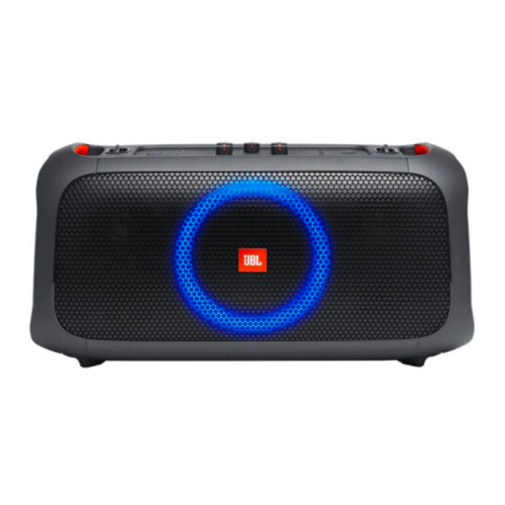
PARTYBOX ON-THE-GO
SKU:JBLPARTYBOXONTHEGOAM,JBLPARTYBOXONTHEGOAS,JBLPARTYBOXONTHEGOCN,JBLPARTYBOXONTHEGOBR,
JBLPARTYBOXONTHEGOEU,JBLPARTYBOXONTHEGOJN,JBLPARTYBOXONTHEGOIN,JBLPARTYBOXONTHEGORU,
JBLPARTYBOXONTHEGOAS2,JBLPARTYBOXONTHEGOBR2,JBLPARTYBOXONTHEGOAS3
Safety Instruction ...................................................................................... 2
Technical Specifications ........................................................................... 5
Software upgrade Instruction & Reset Procedure .................................... 8
Troubleshooting Charts ............................................................................ 9
Disassembly Instruction ...........................................................................10
Block Diagram.......................................................................................... 13
Wiring Diagram ........................................................................................ 14
Circuit Diagarms & PCBA Layout ............................................................ 15
Mechanical Exploded View ...................................................................... 28
Spare Parts List ........................................................................................ 29
Revision List ..............................................................................................31
Released by Global Quality
CONTENTS
harman/kardon, Inc
Service Manual
Rev.1.1 01/2021
Advertisement
Table of Contents

Related Manuals for JBL Partybox On-The-Go


Summary of Contents for JBL Partybox On-The-Go
-
Page 1: Table Of Contents
Service Manual PARTYBOX ON-THE-GO SKU:JBLPARTYBOXONTHEGOAM,JBLPARTYBOXONTHEGOAS,JBLPARTYBOXONTHEGOCN,JBLPARTYBOXONTHEGOBR, JBLPARTYBOXONTHEGOEU,JBLPARTYBOXONTHEGOJN,JBLPARTYBOXONTHEGOIN,JBLPARTYBOXONTHEGORU, JBLPARTYBOXONTHEGOAS2,JBLPARTYBOXONTHEGOBR2,JBLPARTYBOXONTHEGOAS3 CONTENTS Safety Instruction ..................2 Technical Specifications ................5 Software upgrade Instruction & Reset Procedure ........8 Troubleshooting Charts ................9 Disassembly Instruction ................10 Block Diagram..................13 Wiring Diagram ..................14 Circuit Diagarms & PCBA Layout ............15 Mechanical Exploded View .............. - Page 3 Ø Ù Ú Û Ü Ý...
-
Page 5: Technical Specifications
Technical Specifications 4.1 Audio Amplifier Section Set all additional processing (tone controls, equalizers, audio effects, etc) to native or bypass, Unit on Test mode , set digital generator dither off if not additionally defined. Tweeter output resistive load = 6Ω, 2 channels loaded;Woofer output resistive load = 3Ω, 1 channel loaded. - Page 6 4.1.2 Other Requirements Short Circuit Protection at Output Stage The amplifier should be protected so that no functional failure occurs when it is operated with a short across its output stage for 2 minutes. The amplifier should recover after removing the short condition.
- Page 7 4.2.2 Transmitter Performance @BDR Mode Description Specification Maximum Transmit Power @ antenna 9dBm connector Power Control Maximum Power Step <=8dB Minimum Power Step >=2dB Initial Carrier Frequency Shift +/- 75KHz Carrier Drift Drift Rate +/- 20KHz/50us Drift (Single Slot Packet) +/- 25KHz Drift (Three Slot Packet) +/- 40KHz...
-
Page 8: Software Upgrade Instruction &Reset Procedure
Software upgrade Instruction &Reset Procedure 1)Restore factory setting 1: Power on main unit. 2: long press button "volume+" &"play" key for 10 seconds or more at the same time. There will be reset voice prompt output , and main unit reboot. 2)Check software version 1: Power on. -
Page 9: Troubleshooting Charts
Trouble Shooting Party Box On The Go REPAIR CHART NO POWER NO KEY FUNCTION Bluetooth Pairing Failure Function Indicator RGB LED no light up Bluetooth(No sound AUX IN (No Sound USB IN (No Sound Wire_MIC/Guitar(No Sound Wireless MIC (No Sound Press the Power button Press the Power button Press the Power button... -
Page 10: Disassembly Instruction
DISASSEMBLY INSTRUCTIONS Figure 1 Figure 2 Figure 3 Take 4pcs rubber feet bottom apart from Disassembly the bottom 14pcs screw. Disassembly the 5pcs screw from the bottom cover and open the screws. leather back shell and open. Figure 4 Figure 5 Figure 6 Disassembly the rear cover 10pcs screw. - Page 11 DISASSEMBLY INSTRUCTIONS and PCBAS Figure 7 Figure 8 Figure 9 Dismantling 9PCS screws from top cover Take 4pcs side rubber from right side cover Take 4pcs side rubber from left side cover and open screws and open screws Figure 10 Figure 11 Figure 12 Take the top cover nut washev...
- Page 12 Dismantling of lighting PCBA and speaker drivers Figure 13 Figure 14 Figure 15 Dismantling wireless mic Dismantling of power PCBA Dismantling of JK PCBA open wireless mic screws Open jk PCBA screws Open power PCBAS screws Figure 16 Figure 17 Open speaker drivers screws Dismantling of lighting PCBA Open lighting PCBAS screws...
-
Page 13: Block Diagram
Block Diagram TW_L 1. MP3_IN+AC_IN+USB 2layer PCB 2PIN P2.0 Wire Battery Mode: 5W*2 + 15W @1% SPK_OUT(BTL) PT1562A*2 AC_IN Socket 6 10W 3/2PIN/3.96 Wire PSU Mode: 10W*2 + 30W @1% TAS5825P THD 1% PT1562A OP BT603 DET PSU Mode: 15W*2 + 40W @5% D_AMP LRCK 12PIN/2.0 Plug-in connection... -
Page 14: Wiring Diagram
Wiring Diagram External ANT External ANT Internal ANT Wireless_MIC TX DUT Wireless_MIC RX PCB Wireless RX Module Wireless TX Module Wire MIC_IN PCB Guitar PCB CN750 MIC1_DET MIC2 DET MIC1_IN MIC2 IN Guitar Key Board VR1_H CN751 CN753 VR2 H VR1_L VR2 L CN752... -
Page 15: Circuit Diagarms & Pcba Layout
Circuit Diagram-MAIN PCBA C300 L500 AUX_R- 22uF 100MHZ_60 C301 AUX_R+ 22uF C269 0.01uF C302 STB_POWER_CTRL AUX_L- 22uF L501 L300 24733_SCL R203 AUX_L+ C303 22uF 100MHZ_60 R200 DSP3.3 C270 24733_SDA R204 ON_OFF_DET 0.01uF Guitar_in C304 22uF C502 M201 M202 M203 M204 M205 M206 M207... - Page 16 Layout Diagram Bottom view-MAIN PCBA M203 M205 M206 TP407 TP539 C234 TP208 TP428 C276 R2010 TP523 TP206 TP103 TP510 CN211 TP201 C254 TP207 C200 FB200 TP403 C223 C220 R246 FB212 C250 TP516 TP213 FB209 TP518 C230 TP217 M207 C222 R316 C206 CN502 C317...
- Page 17 Layout Diagram TOP view-MAIN PCBA R305 R2014 C365 IC109 IC306 R228 R304 FB404 C501 U200 R221 R275 R301 C409 R300 R253 C433 R2013 R309 IC400 C431 R276 R291 R213 C309 R360 C246 R359 R222 R223 C1020 C366 R358 R364 R236 FB210 R400 C529...
- Page 18 Circuit Diagram-PSU PCBA 56ohm*3 C913 CY902 R926 R925 RHD110300-0010 R924 561P-Y1 L901 470P-500V +18V 10uH R916 R919 R920 R922 FB903 330K 330K 330K 330K CN902 PJE4995L6-8200 D905 C904 RHD200040-0010 CE901 SFN10A300C M222 630V 82U/450V C901 BD901 R910 T901 GBU4K 103/1KV R913 47R PQ3220 D903...
- Page 19 Layout Diagram Bottom view-PSU PCBA P902 FB904 P906 R916 R922 C918 R904 R902 R923 R903 R901 D904 D901 P903 ZD902 R911 R914 D902 P905 R906 P901 IC902 R908 C906...
- Page 20 Layout Diagram TOP view-PSU PCBA CY903 CY904 CY902 G902 LF902 C915 C917 CX901 T901 LF901 F901 CY901 G901 CX902 TVR901 CN901 NTC901...
- Page 21 Circuit Diagram-KEY PCBA VR_TRE VR_BASS VR_Reverb VR_Mic1 VR_Mic2 S3V3 R750 R751 R752 R753 R754 R755 VR_Mic2 VR_Mic1 VR_Reverb BK3V3 S3V3 S3V3 FB750 S3.3V R756 R757 R758 R759 R760 R761 R762 R763 1.GND FB751 2.VR MIC2 FB752 3.VR MIC1 4.VR Reverb FB753 FB754 5.VR BASS...
- Page 22 Layout Diagram Bottom View-KEY PCBA LFA115206-0201 LFA115206-0201 C861 R842 C859 R836 C849 C860 C862 R834 C853 C843 R832 C836 R830 R831 R775 C844 R829 R841 TP784 IC750 R773 R772 C845 R771 R780 R795 R766 C806 R837 IC757 TP795 R840 R764 C805 TP820 FB774...
- Page 23 Layout Diagram TOP View-KEY PCBA SW757 LD759 LD762 LD758 SW750 VR753 SW751 LD757 VR754 LD756 IC751 IC752 LD751 LD755 C826 LD753 C825 C827 R847 C828 C808 C810 C809 LD750 R800 LD763 IC756 IC754 SW753 SW754 SW756 C854 C813 C812 LD754 C811 LD760 C750...
- Page 24 Circuit Diagram-LED +MICI JK +USB AC AUX JK PCBA RGB LED PCB LED1000 LED1001 LED1002 LED1003 LED1004 LED1005 LED1006 LED1007 CN1000 FB1000 5P/1.5mm C750 C751 C752 FB1001 FB1002 FB1003 FB1004 FB1005 FB1006 FB_0603_600 FB1007 FB_0603_600 FB_0603_600 FB_0603_600 FB_0603_600 FB_0603_600 100P 100P 100P FB_0603_600...
- Page 25 Layout Diagram TOP View-LED PCBA Layout Diagram Bottom View-LED PCBA LED1016 FB1017 FB1016 R1015 R1016 C1018 C1019 FB1018 FB1015 R1017 R1014 C1020 C1017 FB1019 FB1014 R1018 C1021 R1013 C1016 FB1020 R1019 C1022 FB1012 R1025 C1023 C1014 R1011 R1020 C1024 C1013 R1010 C1012 R1009...
- Page 26 Layout Diagram Bottom View-MIC PCBA Layout Diagram TOP View-MIC PCBA J700...
- Page 27 Layout Diagram Bottom View-USB-AC-AUX JAKE PCBA Layout Diagram TOP View-USB AC AUX JAKE PCBA...
-
Page 28: Mechanical Exploded View
Part Number SAP Description Usage UoM Pos. No. ABN100008-0306 M FRONT GRILL +FRONT CAB PARTYBOXGO 1 ,2 ABN100008-0309 SKD P TRIM RINGPARTYBOXGO ABN115181-0001 GP SKD RGB LED PCB PARTYBOXGO AUIWD0013-GN01 SPK WOOFER DRIVER PARTYBOXGO AUICT0005-GN05 SPK TWEETER PARTYBOXGO ABN100008-0324 RUBBER FOOT PARTYBOXGO BPB100124-00AA BOTTOM COVER ABS PARTYBOXGO ABN100008-0307... -
Page 29: Spare Parts List
JBL PartyBox on the Go Spare Part List Part Number SAP Description Usage Pos. No. ABN100008-0306 M FRONT GRILL +FRONT CAB PARTYBOXGO 1 ,2 ABN100008-0309 SKD P TRIM RINGPARTYBOXGO ABN115181-0001 GP SKD RGB LED PCB PARTYBOXGO AUIWD0013-GN01 SPK WOOFER DRIVER PARTYBOXGO... - Page 30 LFA115203-0201 2#PCB SPK WIRE PARTYBOXGO GAL100604-1001 AL MAIN PCB BKT R AL ALLOY PARTYBOXGO LFA115205-0201 4# PCB BATTERY WIRE PARTYBOXGO LFA115202-0201 1#PCB BT WIRE PARTYBOXGO WPA128811-0005 BT MODULE 10P MCS-LOGIC PARTYBOXGO ABN100008-0316 P IPAD BKT ABS+PC ASSY PARTYBOXGO ABN100008-0313 P TOP PANEL PARTYBOXGO BRT100091-0101 RUBBER MIC COVER PARTYBOXGO BPK108166-00AA...
-
Page 31: Revision List
REVISION LIST Version 1.0 Date:2020/06/10 Initial release Version 1.1 Date:2021/01/07 Update Spare Part List...
Need help?
Do you have a question about the Partybox On-The-Go and is the answer not in the manual?
Questions and answers