Table of Contents
Advertisement
Quick Links
All manuals and user guides at all-guides.com
1.
PRECAUTION AND NOTICES ------------------------------------------------------------------------------------- 1~2
1.1. SAFETY PRECAUTIONS ---------------------------------------------------------------------------------------- 1
1.2. PRODUCT SAFETY NOTICE ----------------------------------------------------------------------------------- 1
1.3. SERVICE NOTES-------------------------------------------------------------------------------------------------- 1
2.
3.
SPECIFICATIONS ----------------------------------------------------------------------------------------------------- 2~4
3.1.
3.2.
3.3. D-SUB CONNECTOR -------------------------------------------------------------------------------------------- 4
4.
EXPLODED VIEW AND PARTS LIST --------------------------------------------------------------------------- 5~6
4.1. EXPLODED VIEW ------------------------------------------------------------------------------------------------ 5
4.2. EXPLODED VIEW PARTS LIST-------------------------------------------------------------------------------- 6
5.
BLOCK DIAGRAM ---------------------------------------------------------------------------------------------------- 7
6.
SCHEMATIC DIAGRAM -------------------------------------------------------------------------------------------- 8~16
6.1. VGA INPUT -------------------------------------------------------------------------------------------------------- 8
6.2. MV3------------------------------------------------------------------------------------------------------------------ 9
6.3. OUTPUT CONNECTOR ----------------------------------------------------------------------------------------- 10
6.4. MAIN BOARD POWER------------------------------------------------------------------------------------------- 11
6.5. MCU----------------------------------------------------------------------------------------------------------------- 12
6.6. A/D POWER-------------------------------------------------------------------------------------------------------- 13
6.7. PANEL POWER --------------------------------------------------------------------------------------------------- 14
6.8. INVERTER---------------------------------------------------------------------------------------------------------- 15
6.9. CONTENT ---------------------------------------------------------------------------------------------------------- 16
7.
WORKING THEOREM----------------------------------------------------------------------------------------------- 17
8.
WIRING DIAGRAM --------------------------------------------------------------------------------------------------- 18
9.
PCB LAYOUT ----------------------------------------------------------------------------------------------------------- 19~24
9.1. MAIN PCB TOP VIEW ------------------------------------------------------------------------------------------- 19
9.2. MAIN PCB BOTTOM VIEW ------------------------------------------------------------------------------------- 20
9.3. CON PCB TOP VIEW -------------------------------------------------------------------------------------------- 21
9.4. CON PCB BOTTOM VIEW -------------------------------------------------------------------------------------- 22
9.5. POWER PCB TOP VIEW ---------------------------------------------------------------------------------------- 23
9.6. POWER PCB BOTTOM VIEW ---------------------------------------------------------------------------------- 24
10. TROUBLE SHOOTING FLOW CHART ------------------------------------------------------------------------- 25~26
10.1. NO POWER -------------------------------------------------------------------------------------------------------- 25
10.2. NO DISPLAY------------------------------------------------------------------------------------------------------- 26
11. ADJUSTMENT---------------------------------------------------------------------------------------------------------- 27~28
11.1. ADJUSTMENT CONDITIONS AND PRECAUTIONS ------------------------------------------------------- 27
11.2. MAIN ADJUSTMENTS ------------------------------------------------------------------------------------------- 27
11.3. ALIGNMENT PROCEDURES----------------------------------------------------------------------------------- 27
12. ELECTRICAL PARTS LIST ---------------------------------------------------------------------------------------- 29~37
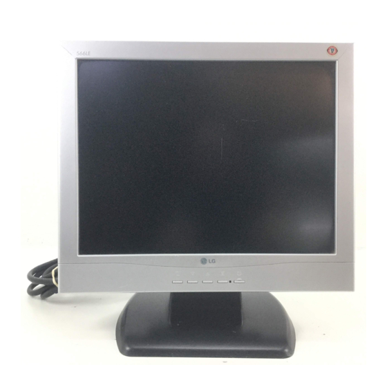
566LE Service Manual
TABLE OF CONTENTS
---------------------------------------------------------- 2
------------------------------------------------------------------------------ 2
---------------------------------------------------------------------------- 3~4
PAGE
7/18/2003
Advertisement
Table of Contents

Subscribe to Our Youtube Channel
Related Manuals for LG 566LE


Summary of Contents for LG 566LE
-
Page 1: Table Of Contents
All manuals and user guides at all-guides.com 566LE Service Manual TABLE OF CONTENTS PAGE PRECAUTION AND NOTICES ------------------------------------------------------------------------------------- 1~2 1.1. SAFETY PRECAUTIONS ---------------------------------------------------------------------------------------- 1 1.2. PRODUCT SAFETY NOTICE ----------------------------------------------------------------------------------- 1 1.3. SERVICE NOTES-------------------------------------------------------------------------------------------------- 1 SERVICE TOOL & EQUIPMENT REQUIRED ---------------------------------------------------------- 2... -
Page 2: Precaution And Notices
All manuals and user guides at all-guides.com 566LE Service Manual 1. PRECAUTION AND NOTICES 1.1. SAFETY PRECAUTIONS This monitor is manufactured and tested on a ground principle that a user's safety comes first. However, improper use or installation may cause damage to the monitor as well as to the user. -
Page 3: Service Tool & Equipment Required
All manuals and user guides at all-guides.com 566LE Service Manual 2. SERVICE TOOL & EQUIPMENT REQUIRED 1. SIGNAL GEN. 2. MULTIMETER 3. OSCILLOSCOPE 4. SCREW DRIVER 5. IRON 6. ABSORBER 7. SOLDER 8. DUMMY LOAD (5ohm/200W) 3. SPECIFICATIONS 3.1. PRODUCT SPECIFICATIONS LCD Panel 15.0"... -
Page 4: Supporting Timing Chart
All manuals and user guides at all-guides.com 566LE Service Manual 3.2. SUPPORTING TIMING CHART ITEM TIMING 720×400@70Hz 640×480@60Hz 640×480@67Hz 640×480@75Hz 800×600@56Hz Pixel Rate 28.322MHz 25.175MHz 30.240MHz 31.500MHz 36.000MHz H TOTAL 31.778us 31.778us 28.571us 26.667us 28.444us H DISPLAY 25.422us 25.422us 21.164us 20.317us... -
Page 5: D-Sub Connector
All manuals and user guides at all-guides.com 566LE Service Manual ITEM TIMING 1024×768@70Hz 1024×768@75Hz Pixel Rate 75.000MHz 78.750MHz H TOTAL 17.707us 16.660us H DISPLAY 13.653us 13.003us H B-Porch 1.920us 2.235us H Width 1.813us 1.219us H Border 0.000us 0.000us V TOTAL 14.272ms... -
Page 6: Exploded View And Parts List
All manuals and user guides at all-guides.com FIG.1 4.1. EXPLODED VIEW (566LE) FIG.3 2C04 X2 5B01 2C03 1F01 5B07 2C05 2C08 2C06 1F03 2C07 V901 2C01 2C05 1F15 X4 MAIN PCB ASS'Y 1F13 2C09 1F14 5B08 5B02 1F04 FIG.1 FIG.2... -
Page 7: Exploded View Parts List
4.2. EXPLODED VIEW PARTS LIST Ref. No. Source Part No. DESCRIPTION SPECIFICATION Q‘TY REMARK 1F01 2024262610 FRONT BEZEL ABS+PC 94V0 PS7604B LG 566LE 1F02 2044261901 FUNCTION KEY JT66LP ASBS 94V0 PS-7604B 1F03 2054252502 ORNAMENT SQR W/O H ABS+PC 94V0 PS-7604B 1F04 2053752201 LED INDIC.-PWR... -
Page 8: Block Diagram
All manuals and user guides at all-guides.com 5. BLOCK DIAGRAM 12V for INVERTER VCOM 3.6V VDDG 18V SWITCHING POWER SUPPLY AC 110~220V DC-DC 5V for system INPUT for PANEL POWER VEEG Q811,Q812,I807, I103,I104,I113 VDDA 9.2V Q801,Q802,Q810, 5V to 3.3V Q804 5V to 2.5V DC_EN VDDD 3.3V... -
Page 9: Schematic Diagram
C108 R108 R106 +3.3V R132 Optional I101C I101D R107 C109 PA-VSYNC VCC 5V C110 C111 0.1UF D112 150PF D111 +3.3V 0 1206 I101E C113 DDC_VCCA 74LVC14 C112 R109 VSYNC 0.1u I102 I101F R110 VCLK DDC-SCL DDC-SDA R111 74LVC14 566LE 7/18/2003... -
Page 10: Mv3
150p 50V J 22000p50V J C137 0.01u 4700p R141 STH1 C141 C143 R158 8.2K C142 R142 4700p 0.01u 4700p BEAD 80 B VAA3RGB C144 C145 C146 0.1u 0.1u 0.1u L113 R144 C219 C220 12MHZ 10u/16V 0.1u X101 C147 C148 566LE 7/18/2003... -
Page 11: Output Connector
47x4 CP10 0.1uF C286 47PX4 0.1uF 47PX4 RP12 47x4 CP11 C285 T_RB0 0.1uF T_RB1 T_RB2 C217 T_RB3 10uF/50V VCOM3.6V T_RB4 T_RB5 T_RB6 C214 T_RB7 10uF/50V VDDD3.3V RB[0..7] RP13 47x4 CP12 47PX4 C215 10uF/50V VDDG18V C216 VEEG-6V 566LE 7/18/2003 -10- 10uF/50V... -
Page 12: Main Board Power
22u / 16V C221 C222 10u/16V 0.1u 100u / 16V 100u / 16V 22u / 16V L106 VAA3RGB L115 VDD2V C171 C121 C174 10u/16V 0.1u C224 10u/16V 0.1u L107 L116 VDC2V C172 C126 C175 C225 10u/16V 0.1u 566LE 7/18/2003 -11-... -
Page 13: Mcu
R356 0.1U 0.1U 0.1U 0.1U 0.1U VOUT 4.7K R331 VCC5V C315 C317 C316 R357 R332 22u / 16V 0.1u 24LC16B R334 R335 Q310 22u / 16V SST3904 R336 Q307 C313 PWM0 R358 10u / 16V SST3904 100K 566LE 7/18/2003 -12-... -
Page 14: A/D Power
374K 1% 1206 R812 2.4K 1% 1206 D813 F801 2.5A/250V Q807 2SC2120 R852 R821 L806 0 1206 D808 R851 4.7K 1206 R850 7A3(6.8V)/DIP 47K 1206 4.7K 1206 D809 C851 Q805 18-2/DIP Q806 10uF/50V 2SC945 S801 AC IN 100~240V 566LE 7/18/2003 -13-... -
Page 15: Panel Power
R834 R843 R835 200mA 1K VR 1.47K/SMD0805 C843 1.15K 1%/SMD0805 100uF/25V C833 D811 1uF/50V C841 EP05QC04/SMD 1uF/50V Q810 F803 2SC945 VDDG18V D815 D818 0.25A/250V dip 40mA EP05QC04/SMD EP05QC04/SMD R838 R837 C848 I805 47uF/50V TL431A R836 18V EN 566LE 7/18/2003 -14-... -
Page 16: Inverter
PDRV_C R880 BAV99 R881 22 C873 100K NDRV_D C874 Q814 D826 1.5N OZ960 2N7002K BAV99 R891 R882 D828 R883 634.1% 825,1% 8.6V 27K,1% R884 Q815 R888 2N7002K 390K,1% C875 Q816 R885 2N3906 0.1U R886 100K R887 51.1K,1% 566LE 7/18/2003 -15-... -
Page 17: Content
M-RESET MCU + POWER VDDCTRL DDC_SCL1 DDC_SCL DDC_SDA1 DDC_SDA BLT_ON PWM0 PWM1 VSYNC HSYNC INV-12V P-KEY MUTE PC_5V BLT_ON1 Y-LED 18V_EN DDC_VCCA B-GND BL-ADJ G-LED VCOM_3.6V DC_EN BLUE VDDD_3.3V G-GND VDDG_18V GREEN VEEG_-6V R-GND DOWN VDDA_9.2 VCC5V 566LE 7/18/2003 -16-... -
Page 18: Working Theorem
All manuals and user guides at all-guides.com 566LE Service Manual 7. WORKING THEOREM A. DC-DC CONVERTER This block provides adjustable output voltages of 9.2V, -6V, 18V and 3 to 4V for the panel. It consists of a Q811 transistor and power switch IC I807 (AIC 1341). -
Page 19: Wiring Diagram
All manuals and user guides at all-guides.com 8. WIRING DIAGRAM (566LE) LCD PANEL P981 P980 P301 P106 P105 P806 P102 P301 MAIN PCB POWER PCB P101 P304 P807 P603 P303 P701 P961 P701 TO:METAL FITTG KEYPAD PCB I/O CABLE... -
Page 20: Pcb Layout
All manuals and user guides at all-guides.com 9. PCB LAYOUT 9.1. MAIN PCB TOP VIEW 566LM/LE 7/18/2003 -19-... -
Page 21: Main Pcb Bottom View
All manuals and user guides at all-guides.com 566LM/LE 7/18/2003 -20-... -
Page 22: Con Pcb Top View
All manuals and user guides at all-guides.com 9.3. CON PCB TOP VIEW 566LM/LE 7/18/2003 -21-... -
Page 23: Con Pcb Bottom View
All manuals and user guides at all-guides.com 566LM/LE 7/18/2003 -22-... -
Page 24: Power Pcb Top View
All manuals and user guides at all-guides.com 9.5. POWER PCB TOP VIEW 566LM/LE 7/18/2003 -23-... -
Page 25: Power Pcb Bottom View
All manuals and user guides at all-guides.com 566LM/LE 7/18/2003 -24-... -
Page 26: Trouble Shooting Flow Chart
All manuals and user guides at all-guides.com 566LE Service Manual 10. TROUBLE SHOOTING FLOW CHART 10.1. NO POWER Start Check D804,Q808, I801,I802,I803 C816 F801 I104 PIN3 Replace I104,I113 Failed? Check Q302,Q8I1,Q812 F802 9.2V Check Q801, C832+ L801,D812,I807 Check 18V on F803... -
Page 27: Display
All manuals and user guides at all-guides.com 566LE Service Manual 10.2. NO DISPLAY Display Dark Amber Check Power Check IO cable is Check I/P signal is in Check LED Color region connect OK ? pwr saving state? Amber & Green... -
Page 28: Adjustment
All manuals and user guides at all-guides.com 566LE Service Manual 11. ADJUSTMENT 11.1. ADJUSTMENT CONDITIONS AND PRECAUTIONS 1. Approximately 30 minutes should be allowed for warm up before proceeding. 2. Adjustments should be undertaken only on those necessary elements since most of them have been carefully preset at the factory. - Page 29 All manuals and user guides at all-guides.com 566LE Service Manual 6500K verify : press “▼” ,“▲” key to move cursor to 6500K at factory mode and press “ 2 “ key, and then check the color temperature is x=0.310 ±0.03 y=0.330 ±...
-
Page 30: Electrical Parts List
All manuals and user guides at all-guides.com 566LE Service Manual 12. ELECTRICAL PARTS LIST When you place a parts order, be sure to indicate the following data on the order: Location No. Parts No. Description LOC NO. SOURCE PART NO. - Page 31 All manuals and user guides at all-guides.com 566LE Service Manual LOC NO. SOURCE PART NO. DESCRIPTION SPECIFICATION REMARK C156 2346410496 CAP,CHIP 85'C CS 0603/Y5V/50V 0.1u C157 2346410496 CAP,CHIP 85'C CS 0603/Y5V/50V 0.1u C163 2346410496 CAP,CHIP 85'C CS 0603/Y5V/50V 0.1u C164...
- Page 32 All manuals and user guides at all-guides.com 566LE Service Manual LOC NO. SOURCE PART NO. DESCRIPTION SPECIFICATION REMARK L106 2379820196 BEAD,HI-IMPEDANCE Z= 200ohm(100MHZ~) 0805 200mA L108 2379820196 BEAD,HI-IMPEDANCE Z= 200ohm(100MHZ~) 0805 200mA L109 2379820196 BEAD,HI-IMPEDANCE Z= 200ohm(100MHZ~) 0805 200mA L110...
- Page 33 All manuals and user guides at all-guides.com 566LE Service Manual LOC NO. SOURCE PART NO. DESCRIPTION SPECIFICATION REMARK RP10 2259247008 RES,CHIP NETWORKS 8P4R 1/16W 47ohm J P=0.8 RP11 2259247008 RES,CHIP NETWORKS 8P4R 1/16W 47ohm J P=0.8 RP12 2259247008 RES,CHIP NETWORKS 8P4R 1/16W 47ohm J P=0.8...
- Page 34 All manuals and user guides at all-guides.com 566LE Service Manual LOC NO. SOURCE PART NO. DESCRIPTION SPECIFICATION REMARK C840 2333610591 CAP,ELE 105'C 1u/ 50V 5*11 P=5.0 C841 2333610591 CAP,ELE 105'C 1u/ 50V 5*11 P=5.0 C842 2333622691 CAP,ELE 105'C 22u/ 50V 5*11 P=5.0...
- Page 35 All manuals and user guides at all-guides.com 566LE Service Manual LOC NO. SOURCE PART NO. DESCRIPTION SPECIFICATION REMARK D824 2364500396 DIODE,ZENER SMD RLZ5.6B 5.45-5.73V 0.5W ROHM D825 2364600996 DIODE,SWITCH SMD BAV99 SOT-23 DIODES D825 2364601096 DIODE,SWITCH SMD BAV99 SOT-23 PHILIPS...
- Page 36 All manuals and user guides at all-guides.com 566LE Service Manual LOC NO. SOURCE PART NO. DESCRIPTION SPECIFICATION REMARK Q306 2360301296 XISTOR,NPN R SMD MMBT3904 DIODES SOT-23 Q307 2360300896 XISTOR,NPN R SMD MMBT3904 FAIRCHILD SOT23 Q307 2360301296 XISTOR,NPN R SMD MMBT3904...
- Page 37 All manuals and user guides at all-guides.com 566LE Service Manual LOC NO. SOURCE PART NO. DESCRIPTION SPECIFICATION REMARK R351 2253327296 RES,CHIP 1/8 RC 0805 1/8 W 2.7Kohm J R353 2253310196 RES,CHIP 1/8 RC 0805 1/8 W 100ohm R354 2253347296 RES,CHIP 1/8 RC 0805 1/8 W 4.7Kohm J...
- Page 38 All manuals and user guides at all-guides.com 566LE Service Manual LOC NO. SOURCE PART NO. DESCRIPTION SPECIFICATION REMARK R866 2251318036 RES,CHIP 1/8 RC 0805 1/8 W 180Kohm F R867 2242330595 H/V RESISTOR RD 1/2W 3.00M R868 2253310396 RES,CHIP 1/8 RC 0805 1/8 W...
Need help?
Do you have a question about the 566LE and is the answer not in the manual?
Questions and answers