Pioneer DV-510K-S Service Manual
Hide thumbs
Also See for DV-510K-S:
- Operating instructions manual (52 pages) ,
- Catalog (10 pages) ,
- Operating instructions manual (52 pages)
Table of Contents
Advertisement
Quick Links
DVD PLAYER
DV-510K-S
DV-510K-K
THIS MANUAL IS APPLICABLE TO THE FOLLOWING MODEL(S) AND TYPE(S).
Model
Type
DV-510K-S
WSXZT5
DV-510K-K
WSXZT5
For details, refer to "Important Check Points for good servicing".
PIONEER CORPORATION
PIONEER ELECTRONICS (USA) INC. P.O. Box 1760, Long Beach, CA 90801-1760, U.S.A.
PIONEER EUROPE NV Haven 1087, Keetberglaan 1, 9120 Melsele, Belgium
PIONEER ELECTRONICS ASIACENTRE PTE. LTD. 253 Alexandra Road, #04-01, Singapore 159936
PIONEER CORPORATION
STANDBY/ON
Power Requirement
AC 220 V to 240V
AC 220 V to 240V
4-1, Meguro 1-chome, Meguro-ku, Tokyo 153-8654, Japan
2008
TOP MENU
MIC1
MIC2
VOLUME
OPEN/CLOSE
MIN — MAX
ENTER
DVD/USB
USB
HOME
MENU
DV-510K-S
Region No.
ORDER NO.
MENU
RRV3779
RETURN
Remarks
5
5
2008 Printed in Japan
T-ZZV MAY
Advertisement
Table of Contents

Related Manuals for Pioneer DV-510K-S


Summary of Contents for Pioneer DV-510K-S
- Page 1 PIONEER CORPORATION 4-1, Meguro 1-chome, Meguro-ku, Tokyo 153-8654, Japan PIONEER ELECTRONICS (USA) INC. P.O. Box 1760, Long Beach, CA 90801-1760, U.S.A. PIONEER EUROPE NV Haven 1087, Keetberglaan 1, 9120 Melsele, Belgium PIONEER ELECTRONICS ASIACENTRE PTE. LTD. 253 Alexandra Road, #04-01, Singapore 159936...
-
Page 2: Safety Information
2. When the cover is open, close viewing through the objective lens with the naked eye will cause exposure to the laser beam. Y/ ON M IC M IC ∗ : See page 26. M IN — M AX /C LO D/ US M EN M EN DV-510K-S... - Page 3 To protect products from damages or failures during transit, the shipping mode should be set or the shipping screws should be installed before shipment. Please be sure to follow this method especially if it is specified in this manual. DV-510K-S...
-
Page 4: Table Of Contents
10.10 POWER PCB ASSY(2/2) ............................64 10.11 WAVEFORMS ................................66 11. PCB CONNECTION DIAGRAM ............................68 11.1 LOADING MOTOR and SW ............................68 11.2 DVD MT PCB ASSY..............................69 11.3 OPERATION PCB ASSY ............................71 11.4 KARAOKE PCB ASSY..............................72 11.5 POWER PCB ASSY..............................73 12. PCB PARTS LIST ................................75 DV-510K-S... -
Page 5: Service Precautions
• Soldering time: Within 3 seconds • Soldering combination: Sn-3.0Ag-0.5Cu • When Soldering/Removing of solder, use the draw in equipment over the Pick Up Unit to prevent the Flux smoke from it. Short circuit using a soldering iron. Pick Up PCB Fig. 1 DV-510K-S... -
Page 6: Disc Removal Method
• Place the unit on a workstation equipped to protect against static electricity, such as conductive mat. • Soldering iron with ground wire or ceramic type is used. • A worker needs to use a ground conductive wrist strap for body. DV-510K-S... -
Page 7: Specifications
2. SPECIFICATIONS 2.1 ACCESSORIES • Remote control x1 • Power cable x1 • Audio / Video cable(1.2m) x1 (red/white/yellow) (076E0PP051) (1206158802) (06CPBA2006) • Dry cell batteries x2 • Warranty Card (AA/R6P) • Operating Instructions DV-510K-S... -
Page 8: Specifications
Wow and flutter ....Limit of measurement (±0.001%W. PEAK) or lower Digital output Coaxial digital output......RCA DV-510K-S... -
Page 9: Disc/Content Format
•DRM (Digital Rights Management) compatible: No (DRM- protected audio files will not play in this player •File extensions: .mp3, .wma, .m4a (these must be used for the player to recognize MP3, WMA and MPEG-4 AAC files–do not use for other file types) Super VCD DV-510K-S... - Page 10 DiviX videos burned on CD-R/-RW/-ROM discs. Keeping the additional compatibility information. same terminology as DVD-Video, individual DivX video files are called “Titles”. When naming files/titles on a CD-R/-RW disc prior to burning, keep in mind that by default they will be played in alphabetical order. DV-510K-S...
-
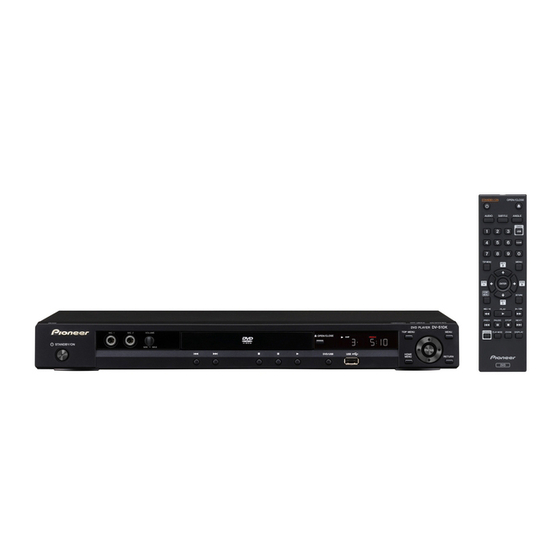
Page 11: Panel Facilitiles
Displays a DVD disc (or DiviX media files) menu VOLUME control —this varies with the disc and may be the same as the ‘top menu’. MIC1/MIC2 input jacks RETURN Returns to the previously displayed menu screen. HOME MENU Display/exit the on-screen display. 10 USB port (Type A) DV-510K-S... - Page 12 KEY (high)/KEY (low) 24 ZOOM ECHO +/- Press to change the zoom level. HOME MENU Display/exit the on-screen display. Use for reverse slow motion playback, frame reverse and reverse scanning. DV-510K-S...
-
Page 13: Basic Items For Service
• Before shipping out the product, be sure to clean the following positions by using the prescribed cleaning tools: Position to be cleaned Position to be cleaned Position to be cleaned Cleaning tools Cleaning tools Cleaning tools Remark Remark Remark Pickup lenses Cleaning liquid : GEM1004 Cleaning paper : GED-008 DV-510K-S... -
Page 14: Pcb Locations
DVD MECHA ASSY DVD MT PCB ASSY OPERATION PCB ASSY Mark No. Description Part No. LIST OF ASSEMBLIES 1..DVD MT PCB ASSY A2L119A130 1..OPERATION PCB ASSY A2L119A270 1..KARAOKE PCB ASSY A2L119ADV0 1..POWER PCB ASSY A2L103A240 1..DVD MECHA ASSY A2L101A650 DV-510K-S... -
Page 15: Jigs List
Lubricants and Glues No. Lubricants and Glues No. Lubricants and Glues No. Remark Remark Remark Daifree GEM1036 (ZLX-ME413A) Refer to "9.3 DVD MECHA SECTION" Grease GYA1001 (ZLB-PN397B) Refer to "9.3 DVD MECHA SECTION" Grease GEM1018 Refer to "9.3 DVD MECHA SECTION" DV-510K-S... -
Page 16: Block Diagram
DVD MT PCB AS (1/6 - 6/6) (A2L119A130) RGB-H CVBS DVD MT PCB PCB130 DMG099 AUDIO L AUDIO R POWER PCB PCB240 DPG017 POWER PCB ASSY (1/2,2/2) (A2L103A240) CP604 CP603 POWER POWER OPERATION PCB ASSY (A2L119A270) TM101 COMMAND TRANSMITTER KARAO DV-510K-S... - Page 17 DESCRIBED IN PARTS LIST ONLY. ATTENTION :LES PIECES REPAREES PAR UN ETANT KARAOKE PCB DANGEREUSES AN POINT DE VUE SECURITE PCBDV0 J6502 VR6501 DEG146 N’UTILISER QUE CELLS DECRITES MIC2 MIC VOL 1 2 3 DANS LA NOMENCLATURE DES PIECES. DV-510K-S...
-
Page 18: Overall Block Diagram
4.2 OVERALL BLOCK DIAGRAM OVERALL BLOCK DIAGRAM DV-510K-S... -
Page 19: Dvd Loader/Mpeg Block Diagram
4.3 DVD LOADER/MPEG BLOCK DIAGRAM DVD LOADER/MPEG BLOCK DIAGRAM DV-510K-S... -
Page 20: Power Block Diagram
4.4 POWER BLOCK DIAGRAM POWER BLOCK DIAGRAM DV-510K-S... -
Page 21: Diagnosis
DECK DOES NOT ACCEPT OPEN/CLOSE Is the voltage at Check P.CON 6V line of pin 8 and 19 of IC2301 POWER BLOCK. about DC6V ? Check CD2302 Is the lose connection connection to DECK. at CD2302 to DECK ? Change DVD LOADER. DV-510K-S... - Page 22 NO PLAYBACK PICTURE OF AV JACK Is there Check IC4001 and a signal at pin 99 of peripheral circuit. IC4001 ? Y es Is there Check J7302 and peripheral video signal at pin 33 circuit. of IC7301 ? Change IC7301. DV-510K-S...
- Page 23 NO ANALOG AUDIO ON PLAYBACK Is there Check J8003 and peripheral AUDIO signal at pins 1 and 7 circuit. of IC8003 ? Is there Check AT pins 116 and 118 AUDIO signal at of IC4001 C8051 and C8053 ? Change IC8003. DV-510K-S...
- Page 24 Any kind of symptoms (no power, a failure in any of the servo, video and audio systems, etc.) may be (DVD MT PCB Assy : IC4001) generated, because the DVD processing is performed by a single chip. 64M SDRAM No power. (DVD MT PCB Assy : IC4005) Block noise is generated during playback. DV-510K-S...
-
Page 25: Method For Diagnosing Degradation Of The Lds On The Pickup Assy
IC2301 Q8020 Q2301 Q2302 C8069 R8076 R8079 C4096 R2309 Q2304 R8084 NR2301 R4017 Q8019 IC4006 Q2301 Q2302 R8057 C2303 Q8018 R4011 R2306 R8085 R8080 C4099 R2307 R2306 B4002 R8083 C4098 C4112 W840 R2307 Q8013 CP4003 CP8003 DMG099A SIDE A DV-510K-S... -
Page 26: Service Mode
• After going into service mode, if you play back the disc, "DISC-NON" is displayed. • The video signal and the audio signal are outputted during the servicemode. • The SKIP key and the SCAN key are effective during the service mode. SERVICE MODE: OFF POWER GGF1381 Service mode remote control unit DV-510K-S... -
Page 27: Service Mode In
LD ON DVD : Press the [TEST] (A8-5E) and [1] (A8-01) keys in order, and turn on the laser diode (650n). : Press the [TEST] (A8-5E) and [4] (A8-04) keys in order, and turn on the laser diode (780n). DV-510K-S... -
Page 28: Display Specification Of The Service Mode
NTSC system : [NTSC] PAL system : [PAL] Automatic setting : [AUTO] Scart terminal output [SK − * *] (Display only the WY model which can do the output setting of scart terminal.) VIDEO : [00] S-VIDEO : [01] DV-510K-S... -
Page 29: Functional Specification Of The Shortcut Key
After you press the A.MON key while holding the ESC key pressed and then input the region number, if the number is different from that set in the unit, an error message is displayed, and the tray opens. DV-510K-S... -
Page 30: Functional Specification Of The Service Mode
-2 : NG 7.0e -4 : NG EDC/ID error history (ID Address, EDC/ID errors, last eight errors) Note: * Error of AV1 is not supported in this player. Indication plan contents Character in bold : Item name : Information display DV-510K-S... -
Page 31: Disassembly
4. Then, pressing the left side back side of the PCB, remove DVD Deck the left side hook of the chassis. Remove the Karaoke PCB in the direction of arrow. Pick Up PCB Karaoke PCB Fig. 1-4 Fig. 1-2 DV-510K-S... - Page 32 PCB and DVD MT PCB connector. 1-5: DVD MT PCB (Refer to Fig. 1-5) Remove the 3 screws (1). Remove the 4 screws (2). Remove the DVD MT PCB in the direction of arrow. DVD MT PCB Fig. 1-5 DV-510K-S...
- Page 33 4. Remove the Traverse Ass'y. Loading Sub Ass'y Loader Sub Ass'y Gear Pulley Insulator (R) Loading Motor PCB Ass’y Traverse Ass'y • Screw Torque: 2.5±0.3kgf•cm (Screw • Screw Torque: 1.0±0.3kgf•cm (Screw Fig. 2-3-A • Screw Torque: 2.0±0.3kgf•cm Fig. 2-2-A DV-510K-S...
- Page 34 3 supports between A and B. Fig. 2-3-D 2. Remove the Plate Clamper, Magnet Clamper and Clamper. Check Hook Check Hook Plate Clamper Magnet Clamper Main Frame Loading Motor PCB Ass’y Check Hook Clamper Fig. 2-3-E Fig. 2-5-A DV-510K-S...
- Page 35 6. Remove the Switch PCB Ass'y. 7. Remove the screw Feed Motor 8. Remove the Gear Feed. 9. Remove the 2 screws 10. Remove the Feed Motor. Safety surface for pressing 11. Remove the Gear Motor. of the insert. Fig. 2-7-C DV-510K-S...
- Page 36 1. When installing the FFC, fold it correctly and install it as shown from Fig. 2-8. NOTE 1. Do not make the folding lines except the specified positions for the FFC. [ 24 pin FFC ] Fold Printing Surface 79 1 mm Reinforcement Plate To Pick Up PCB Fig. 2-8 DV-510K-S...
-
Page 37: Each Setting And Adjustment
While the screen shown at left is being displayed, updating is in progress. DO NOT TURN OFF THE POWER DURING UPDATING. Updating of the firmware is completed. When the screen with the Pioneer logo is displayed, updating is completed. The time required for updating is about 2 minutes. DV-510K-S... - Page 38 2 If updating of the firmware using the disc for updating failed • Was the disc for updating recognized properly? Check if the volume label of the disc is PIONEER. • Is playback of a disc other than the disc for updating possible? If playback of a test CD is also impossible, a reading section, such as PU, may be defective.
- Page 39 DV-510K-S...
-
Page 40: Exploded Views And Parts List
Screws adjacent to b mark on product are used for disassembly. For the applying amount of lubricants or glue, follow the instructions in this manual. (In the case of no amount instructions, apply as you think it appropriate.) 9.1 PACKING DV-510K-S... - Page 41 Gift Sheet 791WHAA183 • • • • • Package 792WHAA252 Gift Box See Contrast table (2) (2) CONTRAST TABLE DV-510K-S/WSXZT5 and DV-510K-K/WSXZT5 are constructed the same except for the following: Mark Symbol and Description DV-510K-S/WSXZT5 DV-510K-K/WSXZT5 Gift Box 793WCDD669 793WCDD699...
-
Page 42: Exterior Section
9.2 EXTERIOR SECTION DV-510K-S... - Page 43 Cushion 65TS10-7.5 8965TS0610 Flat Cable WAL6815038 Screw,Tap Tite(S)-Bind Wash. 816423063U Spring Earth 753WUAA013 (2) CONTRAST TABLE DV-510K-S/WSXZT5 and DV-510K-K/WSXZT5 are constructed the same except for the following: Mark Symbol and Description DV-510K-S/WSXZT5 DV-510K-K/WSXZT5 Cabinet,Top 702WSBA075 702WSBA076 Screw,Tap Tite(B) (3x6.0) 810923060U...
-
Page 44: Dvd Mecha Section
Note : (SW PCB ASS'Y) CD2301 NOTE: Applying positions AA, AB and AC for the CLASS PART NO. MARK grease are displayed for this section. GREASE GEM1018 Check if the correct grease is applied for each GYA1001 position. GEM1036 DV-510K-S... - Page 45 814011723U Rack,Loading 92P100121A Gear,Motor 92P100088A Feed Rack Assy 92AAA0017A Screw,T-Tite(B) (M1.7x5.0 P3) 813381750U Screw,Gear Feed 92P700007A Cord Jumper (CD2301) 12C1061601 Switch (SW1) 0515S32003 Push Switch (SW2) 0500101036 Screw,Tap Tite(P) (2.6x8) 811022680U Sems.Tap Tite(P) (2x8) 816112080U Screw (Bind 2x8) 811022080U DV-510K-S...
-
Page 46: Schematic Diagram
V+1R8 VDD18_USB 33 34 35 36 37 38 39 40 41 42 43 44 45 46 47 48 49 50 51 52 53 54 USB_GND V+3D NOTE:THE DC VOLTAGE EACH PART WAS MEASURED WITH THE DIGITAL TESTER DURING PLAYBACK. DV-510K-S... - Page 47 55 56 57 58 59 60 61 62 63 64 0.01 B JG4091 RXD/SQ R4032 JG4092 TXD/LE R4038 JG4093 JG4094 TP4110 R4075 W825 4.7K PCB130 DMG099 NOTE:THIS SCHEMATIC DIAGRAM IS THE LATEST AT THE TIME OF PRINTING AND SUBJECT TO CHANGE WITHOUT NOTICE DV-510K-S...
-
Page 48: Dvd Mt Pcb Assy(2/6)
FROM POWER PORT FLDC- -28V C4055 FLDC+ V+3E 0.1 B D_GND TP4001 NOTE:THIS SCHEMATIC DIAGRAM IS THE LATEST AT THE TIME NOTE:THE DC VOLTAGE EACH PAR OF PRINTING AND SUBJECT TO CHANGE WITHOUT NOTICE MEASURED WITH THE DIGI DURING PLAYBACK. DV-510K-S... - Page 49 CP4004 B4B-PH-SM4-TB(LF)(SN) USBN USBP USB+5V GND(USB) D4003 L4001 DLP11SN201HL2L AVRL161A1R1NT USBN W831 USBP D4002 (SCHOTTKY 3.0A) AVRL161A1R1NT D4005 W844 USB+5V EC31QS04 CAUTION: DIGITAL TRANSISTOR HE DC VOLTAGE EACH PART WAS EASURED WITH THE DIGITAL TESTER PCB130 DMG099 URING PLAYBACK. DV-510K-S...
-
Page 50: Dvd Mt Pcb Assy(3/6)
FOCS RTN ATTENTION CAUTION :LES PIECES REPAREES PAR UN ETANT :SINCE THESE PARTS MARKED BY DANGEREUSES AN POINT DE VUE SECURITE CRITICAL FOR SAFETY,USE ONES N’UTILISER QUE CELLS DECRITES DESCRIBED IN PARTS LIST ONLY. DANS LA NOMENCLATURE DES PIECES. DV-510K-S... - Page 51 VOFC- VOTK+ VOFC+ PCB130 DMG099 ETANT NOTE:THIS SCHEMATIC DIAGRAM IS THE LATEST AT THE TIME NOTE:THE DC VOLTAGE EACH PART WAS UE SECURITE OF PRINTING AND SUBJECT TO CHANGE WITHOUT NOTICE. MEASURED WITH THE DIGITAL TESTER DURING PLAYBACK. PIECES. DV-510K-S...
-
Page 52: Dvd Mt Pcb Assy(4/6)
GNDA C8051 R8049 NA_P 10K +-1% GNDA MIC IN-H NOTE:THE DC VOLTAGE EACH PART WAS NOTE:THIS SCHEMATIC DIAGRAM IS THE LATEST AT THE TIME MEASURED WITH THE DIGITAL TESTER OF PRINTING AND SUBJECT TO CHANGE WITHOUT NOTICE DURING PLAYBACK. DV-510K-S... - Page 53 MUTE SW R8076 Q8020 47 NA_P 10K +-1% 8.2K +-1% 56P CH YK_P KTC2875-B -1.1 R8077 AUDIO_R R8063 220 +-1% 39K +-1% C8072 R8057 0.1 B AUDIO OUT J8003 RCA-207B(CUSN)-02 HE TIME CAUTION: DIGITAL TRANSISTOR UT NOTICE PCB130 DMG099 DV-510K-S...
-
Page 54: Dvd Mt Pcb Assy(5/6)
FROM POWER PORT 22uH0405 V+5V_A V+5V W889 V+6A TP7303 D_GND D_GND NOTE:THIS SCHEMATIC DIAGRAM IS THE LATEST AT THE TIME NOTE:THE DC VOLTAGE EACH PART WAS MEASURED WITH THE DIGITAL TESTER OF PRINTING AND SUBJECT TO CHANGE WITHOUT NOTICE DURING PLAYBACK. DV-510K-S... - Page 55 FROM/TO POWER VIDEO/AUDIO for 21PIN CP7301 (CP503) IMSA-9604S-12C G/Y_OUT B/U_OUT R/V_OUT P-H/I-L_RGB-H RGB-H ASP/FS CVBS AUDIO L AUDIO R CVBS OUT 4CH BUS SW IC IC7302 SN74CBT3257PWR CVBS/Y/U/V J7302 RCA-405A(CUSN)-08 CAUTION: DIGITAL TRANSISTOR PCB130 DMG099 E TIME T NOTICE DV-510K-S...
-
Page 56: Dvd Mt Pcb Assy(6/6)
GND(USB) USB+5V ATTENTION CAUTION :LES PIECES REPAREES PAR UN ETANT :SINCE THESE PARTS MARKED BY DANGEREUSES AN POINT DE VUE SECURITE CRITICAL FOR SAFETY,USE ONES N’UTILISER QUE CELLS DECRITES DESCRIBED IN PARTS LIST ONLY. DANS LA NOMENCLATURE DES PIECES. DV-510K-S... - Page 57 V_OUT V_ADJ TP4036 R4063 R4072 R4073 +-1% NOTE:THIS SCHEMATIC DIAGRAM IS THE LATEST AT THE TIME NOTE:THE DC VOLTAGE EACH PART WAS PCB130 OF PRINTING AND SUBJECT TO CHANGE WITHOUT NOTICE. MEASURED WITH THE DIGITAL TESTER DMG099 DURING PLAYBACK. DV-510K-S...
-
Page 58: Operation Pcb Assy
SW662 SW663 EVQ11L05R EVQ11L05R -18.0 -18.0 -18.0 -16.0 -16.0 -16.0 -16.0 -16.0 -16.0 -SKIP PAUSE SW664 SW665 EVQ11L05R EVQ11L05R NOTE:THIS SCHEMATIC DIA NOTE:THE DC VOLTAGE EACH PART WAS MEASURED WITH THE DIGITAL TESTER OF PRINTING AND SU DURING PLAYBACK. DV-510K-S... - Page 59 0 -16.0 -16.0 FFC(1.0mm pitch) V+3E V+3E C604 DGND CD601 C605 33P CH 2H0B1202 DGND FLDC+ FLDC+ -28V -28V FLDC- FLDC- V+3E PCB270 DEG149 OTE:THIS SCHEMATIC DIAGRAM IS THE LATEST AT THE TIME OF PRINTING AND SUBJECT TO CHANGE WITHOUT NOTICE. DV-510K-S...
-
Page 60: Karaoke Pcb Assy
JG6502 JG6501 CAUTION ATTENTION :SINCE THESE PARTS MARKED BY :LES PIECES REPAREES PAR UN ETANT CRITICAL FOR SAFETY,USE ONES DANGEREUSES AN POINT DE VUE SECURITE DESCRIBED IN PARTS LIST ONLY N’UTILISER QUE CELLS DECRITES DANS LA NOMENCLATURE DES PIECES DV-510K-S... - Page 61 R6523 R6530 MIC VOL VR6501 EVUE20F15B14 NOTE:THE DC VOLTAGE EACH PART WAS NOTE:THIS SCHEMATIC DIAGRAM IS THE LATEST AT THE TIME PCBDV0 MEASURED WITH THE DIGITAL TESTER OF PRINTING AND SUBJECT TO CHANGE WITHOUT NOTICE DEG146 URITE DURING PLAYBACK. DV-510K-S...
-
Page 62: Power Pcb Assy(1/2)
OF PRINTING AND SUBJECT TO CHANGE WITHOUT NOT DANGEREUSES AN POINT DE VUE SECURITE DESCRIBED IN PARTS LIST ONLY. N’UTILISER QUE CELLS DECRITES NOTE:THE DC VOLTAGE EACH PART WAS DANS LA NOMENCLATURE DES PIECES. MEASURED WITH THE DIGITAL TESTER DURING PLAYBACK. DV-510K-S... - Page 63 Q501 KTC3875S_Y_RTK PCB240 DPG017 S THE LATEST AT THE TIME CAUTION: DIGITAL TRANSISTOR NOTE: THE RESISTOR MARKED F IS FUSE RESISTOR. TO CHANGE WITHOUT NOTICE. THE ALUMI ELECTROLYTIC CAPACITOR MARKED NP T WAS IS NON POLAR ONE. AL TESTER DV-510K-S...
-
Page 64: Power Pcb Assy(2/2)
R8101 DVD_RGB_H_OUT Q8104 4.7K KRC104SRTK NOTE:THIS SCHEMATIC DIAGRAM IS THE LATEST AT THE TIM E NOTE:THE DC VOLTAGE EACH PART WAS CAUTION: DIGITAL T OF PRINTING AND SUBJECT TO CHANGE WITHOUT NOTICE. MEASURED WITH THE DIGITAL TESTER DURING PLAYBACK. DV-510K-S... - Page 65 CVBS_VIDEO_OUT 6.3V 1000 YK_P +-1% 1/10W DVD_RGB_H_OUT Q8105 KRA102SRTK R8109 D_RGB_H_OUT Q8104 68 1/10W +-1% C104SRTK * The parts except mark cannot be changed. On that occasion, replace whole Assy. CAUTION: DIGITAL TRANSISTOR CAUTION: DIGITAL TRANSISTO R PCB240 DPG017 DV-510K-S...
-
Page 66: Waveforms
Note : The encircled numbers denote measuring point in the schematic diagram. DVD MT PCB ASSY POWER PCB ASSY MPEG/MICON/DSP 21PIN/D-TERMINAL/DIGITAL J8001-pin2 (Coaxial Out) IC4001-pin9 (XTALI) V:500mV/div. H:200ns/div. IC4001-pin66 (SDCLK) V:0.5V/div. H:2ns/div. IC4001-pin93 (SPDIF) V:1.0V/div. H:200ns/div. AUDIO JACK J8003-pin3 (Lch_Out) J8003-pin2 (Rch_Out) DV-510K-S... - Page 67 POWER PCB ASSY OPERATION PCB ASSY DISPLAY DV-510K-S...
-
Page 68: Pcb Connection Diagram
Field effect SIDE B P.C.Board Chip Part transistor Resistor array 3-terminal regulator 11.1 LOADING MOTOR and SW SIDE A SIDE A LOADING MOTOR (INSERTED PARTS) DED020A M2602 M2601 SIDE B SIDE B LOADING MOTOR (CHIP MOUNTED PARTS) M2603 CD2302 DV-510K-S... -
Page 69: Dvd Mt Pcb Assy
W802 C8067 R2319 R7317 W832 C7322 IC8003 IC2301 Q8020 C8069 R8076 R8079 C4096 R2309 Q2304 R8084 R4017 NR2301 Q8019 IC4006 Q2301 Q2302 R8057 Q8018 R4011 R2306 R8085 C4099 R2307 R8080 B4002 R8083 C4098 W840 C4112 Q8013 CP8003 CP4003 DMG099A DV-510K-S... - Page 70 SIDE B SIDE B DVD MT PCB ASSY W849 R4038 R4032 R4068 R4030 W824 W836 W831 Q4003 W813 IC4007 R2343 R2341 W834 D2301 D2302 W822 R4001 W821 W833 DMG099A Q2306 W845 DV-510K-S...
-
Page 71: Operation Pcb Assy
C654 W005 W011 W006 W009 D667 D668 C601 C605 W007 W012 C675 W013 W014 W017 C676 C610 R656 W016 C608 R658 D652 R657 D654 C611 R655 D655 B601 D656 D657 W019 W020 D665 W018 C613 C604 CP604 C651 R666 DV-510K-S... -
Page 72: Karaoke Pcb Assy
11.4 KARAOKE PCB ASSY SIDE A SIDE A KARAOKE PCB ASSY SIDE B SIDE B KARAOKE PCB ASSY IC6503 IC6504 IC6501 DV-510K-S... -
Page 73: Power Pcb Assy
C538 C521 W015 D527 L503 IC501 C536 C8115 C520 W004 W019 R514 C522 A30C5 C8114 C528 R510_1 D528 Q502 L505 W819 C526 D521 W009 C8112 W010 W011 Q504 C517 L8101 D8101 D8104 CP502 D536 D531 D535 C519 D533 C8113 DV-510K-S... - Page 74 SIDE B SIDE B POWER PCB ASSY DV-510K-S...
-
Page 75: Pcb Parts List
8003 RCA JACK 060R451012 X 4001 CRYSTAL (27MHz) 100GT02720 OPERATION PCB ASSY SEMICONDUCTORS IC 651 IC PT6315 IF4K063150 SWITCHES SW 652-667SWITCH TACT 0504R01T38 OTHERS CP 602 CONNECTOR PCB SIDE 06G5AA1002 V 651 TUBE FLUORESCENT 096F80R401 OS 651 REMOTE RECEIVER 077Q040004 DV-510K-S...
Need help?
Do you have a question about the DV-510K-S and is the answer not in the manual?
Questions and answers