Table of Contents
Advertisement
Quick Links
DVD PLAYER
DV-500K-S
THIS MANUAL IS APPLICABLE TO THE FOLLOWING MODEL(S) AND TYPE(S).
Model
Type
DV-500K-S
TLXZT
DV-500K-S
TLXZT3
For details, refer to "
PIONEER CORPORATION
PIONEER ELECTRONICS (USA) INC. P.O. Box 1760, Long Beach, CA 90801-1760, U.S.A.
PIONEER EUROPE NV Haven 1087, Keetberglaan 1, 9120 Melsele, Belgium
PIONEER ELECTRONICS ASIACENTRE PTE. LTD. 253 Alexandra Road, #04-01, Singapore 159936
PIONEER CORPORATION 2007
Power Requirement
AC 110 V to 240 V
AC 110 V to 240V
Important Check Points for Good Servicing
4-1, Meguro 1-chome, Meguro-ku, Tokyo 153-8654, Japan
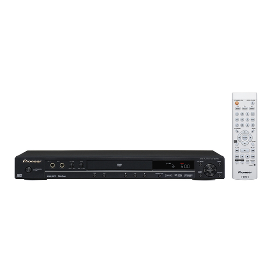
STANDBY/
ON
OPEN/CLOSE
DV-500K-S
Region No.
" .
ORDER NO.
TOP MENU
MENU
RRV3591
ENTER
HOME
MENU
RETURN
Remarks
3
3
T-ZZV APR. 2007 printed in Japan
Advertisement
Table of Contents

Related Manuals for Pioneer DV-500K-S


Summary of Contents for Pioneer DV-500K-S
- Page 1 PIONEER CORPORATION 4-1, Meguro 1-chome, Meguro-ku, Tokyo 153-8654, Japan PIONEER ELECTRONICS (USA) INC. P.O. Box 1760, Long Beach, CA 90801-1760, U.S.A. PIONEER EUROPE NV Haven 1087, Keetberglaan 1, 9120 Melsele, Belgium PIONEER ELECTRONICS ASIACENTRE PTE. LTD. 253 Alexandra Road, #04-01, Singapore 159936 PIONEER CORPORATION 2007 T-ZZV APR.
-
Page 2: Safety Information
2. When the cover is open, close viewing through the objective lens with the naked eye will cause exposure to the laser beam. ∗ : See page 28. /C LO M EN M EN DV-500K-S... - Page 3 To protect products from damages or failures during transit, the shipping mode should be set or the shipping screws should be installed before shipment. Please be sure to follow this method especially if it is specified in this manual. DV-500K-S...
-
Page 4: Table Of Contents
11. PCB CONNECTION DIAGRAM ........................67 11.1 LOADING MOTOR/SW .......................... 67 11.2 DVD MT PCB ASSY..........................68 11.3 OPERATION 1 PCB and OPERATION 2 PCB ASSYS................70 11.4 POWER PCB ASSY..........................71 11.5 KARAOKE PCB ASSY........................... 73 12. PCB PARTS LIST ............................74 DV-500K-S... -
Page 5: Service Precautions
• Soldering time: Within 3 seconds • Soldering combination: Sn-3.0Ag-0.5Cu • When Soldering/Removing of solder, use the draw in equipment over the Pick Up Unit to prevent the Flux smoke from it. Short circuit using a soldering iron. Pick Up PCB Fig. 1 DV-500K-S... -
Page 6: Disc Removal Method
• Place the unit on a workstation equipped to protect against static electricity, such as conductive mat. • Soldering iron with ground wire or ceramic type is used. • A worker needs to use a ground conductive wrist strap for body. DV-500K-S... -
Page 7: Specifications
2. SPECIFICATIONS 2.1 ACCESSORIES Accessories • Remote control ×1 • Power cable ×1 • Audio / Video cable(1.2m) ×1 (1206158802) (red/white/yellow) (07650LE030) (06CPBA2006) • Dry cell batteries ×2 ENTER • Warranty Card (AA/R6P) • Operating Instructions DV-500K-S... -
Page 8: Specifications
Number of channels ..... 2 Jacks ......RCA DV-500K-S... -
Page 9: Disc/Content Format
DVD-R/RW compatibility • Compatible formats: DVD-Video, Video Recording (VR)* * Edit points may not play exactly as edited; Super VCD screen may go momentarily blank at edited points. • Unfinalized playback: No • WMA/MP3/JPEG file playback on DVD-R/ RW: No DV-500K-S... - Page 10 In these particular instances, check with the software publisher for more detailed information. Discs recorded in packet write mode (UDF format) are not compatible with this player. Check the DVD-R/RW or CD-R/RW software disc boxes for additional compatibility information. DV-500K-S...
-
Page 11: Panel Facilities
Adjust the amount of echo effect added to the OPEN/CLOSE vocals Press to open or close the disc tray. 16 VOLUME control Controls onlythe level of the microphone(s). Press to start or resume playback. 17 MIC 1/MIC2 input jacks DV-500K-S... - Page 12 Press to pause playback; press again to restart. (low) • Press (low) repeatedly to lower the pitch of the backing music. (high) • Press (high) repeatedly to raise the pitch of the backing music. DV-500K-S...
- Page 13 Press to display information about the disc Press to display a DVD disc menu, or the playing. Disc Navigator if a VR format DVD-RW, CD, Video CD , MP3, WMA or JPEG disc is 24 ZOOM loaded. Press to change the zoom level. DV-500K-S...
-
Page 14: Basic Items For Service
Items to be checked regarding video Item to be checked regarding audio Block noise Distortion Horizontal noise Noise Dot noise Volume too low Disturbed image (video jumpiness) Volume too high Too dark Volume fluctuating Too bright Sound interrupted Mottled color DV-500K-S... -
Page 15: Pcb Locations
OPERATION 1 PCB ASSY Mark No. Description Part No. LIST OF ASSEMBLIES 1..DVD MT PCB ASSY A2K020A130 1..OPERATION 1 PCB ASSY A2K020A270 1..OPERATION 2 PCB ASSY A2K001A280 1..POWER PCB ASSSY A2K020A240 1..KARAOKE PCB ASSSY A2K020ADV0 1..DVD MECHA ASSY A2K001A650 DV-500K-S... -
Page 16: Jigs List
• Before shipping out the product, be sure to clean the following positions by using the prescribed cleaning tools: Position to be cleaned Position to be cleaned Cleaning tools Cleaning tools Remark Remark Pickup leneses Cleaning liquid : GEM1004 Cleaning paper : GED-008 DV-500K-S... - Page 17 DV-500K-S...
-
Page 18: Block Diagram
ATTENTION CAUTION :LES PIECES REPAREES PAR UN ETANT DANGEREUSES AN POINT DE VUE :SINCE THESE PARTS MARKED BY ARE CRITICAL FOR SAFETY, SECURITE N'UTILISER QUE CELLS DECRITES DANS LA NOMENCLATURE DES PIECES USE ONES DESCRIBED IN PARTS LIST ONLY DV-500K-S... - Page 19 2H051602 M2603 LOADING MOTOR(-) LOAD- BCZ3B05 LOADING MOTOR(-) LOAD+ OPEN SW-1(OPEN) GND(SW) SSS-28-5 CLOSE SW-2(CLOSE) PCB610 DVD PCB DED021 PCB130 DMF089 NOTE: THIS INTERCONNECTION DIAGRAM IS THE LATEST AT THE TIME OF PRINTING AND SUBJECT TO CHANGE WITHOUT NOTICE DV-500K-S...
-
Page 20: Overall Block Diagram
4.2 OVERALL BLOCK DIAGRAM DV-500K-S... -
Page 21: Dvd Loader Block Diagram
4.3 DVD LOADER BLOCK DIAGRAM DV-500K-S... -
Page 22: Power Block Diagram
4.4 POWER BLOCK DIAGRAM DV-500K-S... -
Page 23: Diagnosis
DECK DOES NOT ACCEPT OPEN/CLOSE Is the voltage at Check P.CON 6V line of pin 8 and 19 of IC2301 POWER BLOCK. about DC6V ? Check CD2302 Is the lose connection connection to DECK. at CD2302 to DECK ? Change DVD LOADER. DV-500K-S... - Page 24 Replace V651 or IC651. NO PLAYBACK PICTURE OF AV JACK Is there Check IC4001 and a signal at pin 164 of peripheral circuit. IC4001 ? Is there Check J7302 and peripheral video signal at pin 33 circuit. of IC7301 ? Change IC7301. DV-500K-S...
- Page 25 NO ANALOG AUDIO ON PLAYBACK Is there Check J8003 and peripheral AUDIO signal at pins 1 and 7 circuit. of IC8003 ? Is there Check AT pins 184 and AUDIO signal at C8051 186 of IC4001. and C8053 ? Change IC8003. DV-500K-S...
- Page 26 Any kind of symptoms (no power, a failure in any of the servo, video and audio systems, etc.) may be (DVD MT PCB Assy : IC4001) generated, because the DVD processing is performed by a single chip. 64M SDRAM No power. (DVD MT PCB Assy : IC4005) Block noise is generated during playback. DV-500K-S...
-
Page 27: Method For Diagnosing Degradation Of The Lds On The Pickup Assy
No playback of a CD : Measure the voltage between the two ends of R2320 or R2322 on the DVDM Assy. If the voltage is 0.4 V or higher, the 780-nm LD is degraded. DVD MT PCB ASSY Front side SIDE A DV-500K-S... -
Page 28: Service Mode
• After going into service mode, if you play back the disc, "DISC-NON" is displayed. • The video signal and the audio signal are outputted during the servicemode. • The SKIP key and the SCAN key are effective during the service mode. SERVICE MODE: OFF POWER GGF1381 Service mode remote control unit DV-500K-S... -
Page 29: Service Mode In
3 LD ON DVD : Press the [TEST] (A8-5E) and [1] (A8-01) keys in order, and turn on the laser diode (650n). : Press the [TEST] (A8-5E) and [4] (A8-04) keys in order, and turn on the laser diode (780n). DV-500K-S... -
Page 30: Display Specification Of The Service Mode
: [NTSC] PAL system : [PAL] Automatic setting : [AUTO] Scart terminal output [SK – ∗ ∗] (Display only the WY model which can do the output setting of scart terminal.) VIDEO : [00] S-VIDEO : [01] : [02] DV-500K-S... -
Page 31: Functional Specification Of The Shortcut Key
• Region confirmation mode (ESC + A.MON [Service mode remote control unit] + "1"-"8" [Service mode remote control unit] keys) After you press the A.MON key while holding the ESC key pressed and then input the region number, if the number is different from that set in the unit, an error message is displayed, and the tray opens. DV-500K-S... -
Page 32: Functional Specification Of The Service Mode
%%e -2 : NG 7.0e -4 : NG 3 EDC/ID error history (ID Address, EDC/ID errors, last eight errors) Note: ∗ Error of AV1 is not supported in this player. Indication plan contents Character in bold : Item name : Information display DV-500K-S... -
Page 33: Disassembly
When installing the DVD Deck, remove all the soldering Remove the screw 1. on the short circuit position after the connection of Pick Remove the 4 screws 2. UpPCB and DVD MT PCB connector. Remove the Power PCB in the direction of arrow. DV-500K-S... - Page 34 1-5: DVD MT PCB (Refer to Fig. 1-5) Remove the 5 screws 1. Remove the 4 screws 2. Remove the DVD MT PCB in the direction of arrow. DVD MT PCB Fig. 1-5 DV-500K-S...
-
Page 35: Dvd Deck Section
Loader Sub Ass'y Gear Pulley Loading Motor Insulator (R) Loading Motor PCB Ass’y Traverse Ass'y • Screw Torque: 2.5 ± 0.3kgf•cm (Screw 1) • Screw Torque: 1.0 ± 0.3kgf•cm (Screw 2) Fig. 2-3-A • Screw Torque: 2.0 ± 0.3kgf•cm Fig. 2-2-A DV-500K-S... - Page 36 3 supports 1. between A and B. Fig. 2-3-D 2. Remove the Plate Clamper, Magnet Clamper and Clamper. Check Hook Check Hook Plate Clamper Magnet Clamper Main Frame Loading Motor PCB Ass’y Check Hook Clamper Fig. 2-3-E Fig. 2-5-A DV-500K-S...
- Page 37 6. Remove the Switch PCB Ass'y. 7. Remove the screw 4. Feed Motor 8. Remove the Gear Feed. 9. Remove the 2 screws 5. 10. Remove the Feed Motor. Safety surface for pressing 11. Remove the Gear Motor. of the insert. Fig. 2-7-C DV-500K-S...
- Page 38 Fig. 2-8. NOTE 1. Do not make the folding lines except the specified positions for the FFC. [ 24 pin FFC ] Fold Printing Surface 79 ± 1 mm Reinforcement Plate To Pick Up PCB Fig. 2-8 DV-500K-S...
-
Page 39: Each Setting And Adjustment
While the screen shown at left is being displayed, updating is in progress. DO NOT TURN OFF THE POWER DURING UPDATING. 4 Updating of the firmware is completed. When the screen with the Pioneer logo is displayed, updating is completed. The time required for updating is about 2 minutes. DV-500K-S... - Page 40 2 If updating of the firmware using the disc for updating failed • Was the disc for updating recognized properly? Check if the volume label of the disc is PIONEER. • Is playback of a disc other than the disc for updating possible? If playback of a test CD is also impossible, a reading section, such as PU, may be defective.
- Page 41 DV-500K-S...
-
Page 42: Exploded Views And Parts List
For the applying amount of lubricants or glue, follow the instructions in this manual. (In the case of no amount instructions, apply as you think it appropriate.) 9.1 PACKING SECTION TLXZT3 Only TLXZT3 Only DV-500K-S... - Page 43 See Contrast Table(2) Operating Instructions J2K00201A (English) Operating Instructions J2K00210A (Chinese) (2) CONTRAST TABLE DV-500K-S/TLXZT and /TLXZT3 types are constructed the same except for the following : Mark No. Symbol and Description DV-500K-S/TLXZT DV-500K-S/TLXZT3 14 Carton Label Not Used 723000D561...
-
Page 44: Exterior Section
9.2 EXTERIOR SECTION NON-CONTACT SIDE CONTACT SIDE DV-500K-S... - Page 45 • • • • • • Screw,Tap Tite(S)-Bind Wash. 816423063U Screw,Tap Tite(S) (3x5.5) 8107D3055U (2) CONTRAST TABLE DV-500K-S/TLXZT and /TLXZT3 types are constructed the same except for the following : Mark No. Symbol and Description DV-500K-S/TLXZT DV-500K-S/TLXZT3 Sheet, Caution 726000A142...
-
Page 46: Dvd Mecha Section
Note : (SW PCB ASS'Y) CD2301 NOTE: Applying positions AA, AB and AC for the CLASS PART NO. MARK grease are displayed for this section. GREASE GEM1018 Check if the correct grease is applied for each GYA1001 position. GEM1036 DV-500K-S... - Page 47 92P100088A Feed Rack Assy 92AAA0017A Screw,T-Tite(B) (M1.7x5.0 P3) 813381750U Screw,Gear Feed 92P700007A Cord Jumper (CD2301) 122H061605 Switch (SW1) 0515S32003 Push Switch (SW2) 0500101036 Screw,Tap Tite(P) (2.6x8) 811022680U Sems.Tap Tite(P) (2x8) 816112080U Screw (Bind 2x8) 811022080U DVD MECHA ASSY A2K001A650 DV-500K-S...
-
Page 48: Schematic Diagram
55 56 57 58 59 60 61 62 63 64 65 66 67 68 69 70 71 72 73 74 75 76 77 78 79 80 81 82 83 84 85 86 87 88 DQ11 DQ12 DQ13 DQ14 DQ15 DBA0 DBA1 R4034 R4036 R4037 R4039 MA10 MA11 SDCKE SDCLK 1.8V B4011 MMZ1608R102CT NOTE:THE DC VOLTAGE EACH PART WAS MEASURED WITH THE DIGITAL TESTER DURING PLAYBACK. DV-500K-S... - Page 49 TP4091 R4037 10K TP4035 TP4092 R4075 R4039 10K RESET TP4093 TP4094 C4118 (V+3D) 100P CH NR4001 4D03WGJ0330T5E PCB130 B4011 R4076 DMF089 MMZ1608R102CT NOTE:THIS SCHEMATIC DIAGRAM IS THE LATEST AT THE TIME OF PRINTING AND SUBJECT TO CHANGE WITHOUT NOTICE DV-500K-S...
-
Page 50: Dvd Mt Pcb Assy(2/6)
0.001 B DQM0 C4040 DCAS# DRAS# DBA1 DBA0 NC (WP#/ACC) SDCLK DCS# RY/BY# PRD# PCE# PRD# PCE# PWR# FROM POWER PORT (V+3D) D_GND NOTE:THIS SCHEMATIC DIAGRAM IS THE LATEST AT THE TIME OF PRINTING AND SUBJECT TO CHANGE WITHOUT NOTICE DV-500K-S... - Page 51 DQM0 NC/RFU LDQM DQM1 DWE# UDQM SDCLK DCAS# CAS# SDCKE DRAS# RAS# DCS# MA11 DBA0 BA0/A13 DBA1 BA1/A12 MA10 A10/AP C4055 0.1 B TP4001 NOTE:THE DC VOLTAGE EACH PART WAS PCB130 MEASURED WITH THE DIGITAL TESTER DMF089 DURING PLAYBACK. DV-500K-S...
-
Page 52: Dvd Mt Pcb Assy(3/6)
W802 C2311 ATTENTION CAUTION :LES PIECES REPAREES PAR UN ETANT :SINCE THESE PARTS MARKED BY DANGEREUSES AN POINT DE VUE SECURITE CRITICAL FOR SAFETY,USE ONES N'UTILISER QUE CELLS DECRITES DESCRIBED IN PARTS LIST ONLY DANS LA NOMENCLATURE DES PIECES DV-500K-S... - Page 53 3.03 VOTK- VOFC- 2.82 2.63 VOTK+ VOFC+ PCB130 NOTE:THE DC VOLTAGE EACH PART WAS NOTE:THIS SCHEMATIC DIAGRAM IS THE LATEST AT THE TIME DMF089 OF PRINTING AND SUBJECT TO CHANGE WITHOUT NOTICE MEASURED WITH THE DIGITAL TESTER DURING PLAYBACK. DV-500K-S...
-
Page 54: Dvd Mt Pcb Assy(4/6)
:SINCE THESE PARTS MARKED BY :LES PIECES REPAREES PAR UN ETANT MEASURED WITH THE DIGITAL TESTER CRITICAL FOR SAFETY,USE ONES DANGEREUSES AN POINT DE VUE SECURITE DURING PLAYBACK. DESCRIBED IN PARTS LIST ONLY N'UTILISER QUE CELLS DECRITES DANS LA NOMENCLATURE DES PIECES DV-500K-S... - Page 55 R8061 C8067 C8070 68P CH YK_P R8063 +-1% C8072 AUDIO OUT R8057 J8003 RCA-207B-02 NOTE:THIS SCHEMATIC DIAGRAM IS THE LATEST AT THE TIME CAUTION: DIGITAL TRANSISTOR CAUTION: DIGITAL TRANSISTOR PCB130 DMF089 OF PRINTING AND SUBJECT TO CHANGE WITHOUT NOTICE DV-500K-S...
-
Page 56: Dvd Mt Pcb Assy(5/6)
FROM POWER PORT 22uH 0405 V+5V_A V+5V TP7303 D_GND D_GND NOTE:THIS SCHEMATIC DIAGRAM IS THE LATEST AT THE TIME NOTE:THE DC VOLTAGE EACH PART WAS MEASURED WITH THE DIGITAL TESTER OF PRINTING AND SUBJECT TO CHANGE WITHOUT NOTICE DURING PLAYBACK. DV-500K-S... - Page 57 W877 TP7301 W801 S_C OUT S_Y OUT CVBS OUT CVBS/Y/U/V S-VIDEO OUT J7302 J7301 RCA-405A-08 DIN-409A CAUTION: DIGITAL TRANSISTOR PCB130 DMF089 DV-500K-S...
-
Page 58: Dvd Mt Pcb Assy(6/6)
FL DC+ -28V ATTENTION CAUTION :LES PIECES REPAREES PAR UN ETANT :SINCE THESE PARTS MARKED BY DANGEREUSES AN POINT DE VUE SECURITE CRITICAL FOR SAFETY,USE ONES N'UTILISER QUE CELLS DECRITES DESCRIBED IN PARTS LIST ONLY DANS LA NOMENCLATURE DES PIECES DV-500K-S... - Page 59 FLDC- FLDC+ -28V D_GND TO MEMORY D_GND PCB130 DMF089 NOTE:THIS SCHEMATIC DIAGRAM IS THE LATEST AT THE TIME NOTE:THE DC VOLTAGE EACH PART WAS OF PRINTING AND SUBJECT TO CHANGE WITHOUT NOTICE MEASURED WITH THE DIGITAL TESTER DURING PLAYBACK. DV-500K-S...
-
Page 60: Operation 1 And Operation 2 Pcb Assys
GR10 LED2 EVQ11L05R -18.0 GR11 LED1 PCB280 DEF129 -18.0 -18.0 -18.0 -16.0 -16.0 -16.0 -16.0 -16.0 -16.0 OS651 C659_1 ROM-V340TAO 100P CH Vout R666 1/4W S801Y NOTE:THE DC VOLTAGE EACH PART WAS MEASURED WITH THE DIGITAL TESTER DURING PLAYBACK. DV-500K-S... - Page 61 CD601 V+3E 2H0B1003 V+3E V+3E C604 DGND C605 33P CH DGND TP663 0.001 B FLDC+ FLDC+ -28V -28V FLDC- FLDC- NOTE:THIS SCHEMATIC DIAGRAM IS THE LATEST AT THE TIME PCB270 OF PRINTING AND SUBJECT TO CHANGE WITHOUT NOTICE DEF126 DV-500K-S...
-
Page 62: Power Pcb Assy
:SINCE THESE PARTS MARKED BY :LES PIECES REPAREES PAR UN ETANT OF PRINTING AND SUBJECT TO CHANGE WITHOUT NOTICE CRITICAL FOR SAFETY,USE ONES DANGEREUSES AN POINT DE VUE SECURITE DESCRIBED IN PARTS LIST ONLY N'UTILISER QUE CELLS DECRITES DANS LA NOMENCLATURE DES PIECES DV-500K-S... - Page 63 DPF015 PROTECT Q501 KTC3875S_Y_RTK CAUTION: DIGITAL TRANSISTOR NOTE: THE RESISTOR MARKED F IS FUSE RESISTOR. NOTE:THE DC VOLTAGE EACH PART WAS OTICE MEASURED WITH THE DIGITAL TESTER THE ALUMI ELECTROLYTIC CAPACITOR MARKED NP DURING PLAYBACK. IS NON POLAR ONE. DV-500K-S...
-
Page 64: Karaoke Pcb Assy
KA_P ECHO C6509 R6515 R6517 LPF1 8.2K D6505 KA_P LPF1 O C6512 R6518 UDZS5.1B 0.012 B OP1 O C6521 OP1 IN 0.01 MUTE R6521 CLOC 120K NOTE:THE DC VOLTAGE EACH PART WAS MEASURED WITH THE DIGITAL TESTER DURING PLAYBACK. DV-500K-S... - Page 65 OP1 IN OP2 IN 0.01 0.01 C6531 KA_P C6532 MUTE ECHO VOL 0.01 R6521 CLOCK 120K W803 ECHO VOL VR6502 EVUE20F15B14 PCBDV0 NOTE:THIS SCHEMATIC DIAGRAM IS THE LATEST AT THE TIME DEF105 OF PRINTING AND SUBJECT TO CHANGE WITHOUT NOTICE DV-500K-S...
-
Page 66: Wave Forms
J7302-pin6 (CVBS_Out) J7301-pin4 (S_C_Out) VIDEO JACK V:1.0V/div. H:200nsec/div. V:200mV/div. H:10µsec/div. V:500mV/div. H:10µsec/div. CP4002-pin1 (FP_SCK) J7302-pin5 (Y_Out) V:1.0V/div. H:20µsec/div. V:500mV/div. H:10µsec/div. OPERATION 1 PCB ASSY IC651-pin5 (OSC) DISPLAY V:500mV/div. H:1µsec/div. J8003-pin3 (Lch_Out) J7302-pin3 (U_Out) AUDIO JACK V:1.0V/div. H:500µsec/div. V:500mV/div. H:20µsec/div. DV-500K-S... -
Page 67: Pcb Connection Diagram
B C E Field effect SIDE B P.C.Board Chip Part transistor Resistor array 3-terminal regulator 11.1 LOADING MOTOR/SW LOADING MOTOR (INSERTED PARTS) LOADING MOTOR (CHIP MOUNTED PARTS) SOLDER SIDE SOLDER SIDE DED021A M2603 CD2302 SOLDER SIDE DED020A M2602 M2601 DV-500K-S... -
Page 68: Dvd Mt Pcb Assy
R2311 C2317_1 C8067 R2319 R2329 R7317 IC8003 IC2301 C8069 C4096 R8079 R2322 R8084 W806 Q8019 IC4006 Q2304 R8057 Q2301 C4094 Q8013 Q8018 Q2302 CP2303 R8085 R8080 C4099 B4002 Q2306 C2301 Q2307 C4098 R8052 C4112 W840 R8053 CP2301 CP8003 CP4003 DV-500K-S... - Page 69 SIDE B SIDE B DVD MT PCB ASSY DMF089A R2341 R2343 W834 R4001 W821 R2325 W822 R8058 R8060 W833 R8059 R8014 R2308 R8051 W814 R8044 DV-500K-S...
-
Page 70: Operation 1 Pcb And Operation 2 Pcb Assys
SW652 SW653 SW659 W809 SW661 SW658 W007 W009 W003 OPERATON 2 PCB ASSY D664 (CHIP MOUNTED PARTS) D668 W011 W012 W013 W010 OPERATON 2 SW666 PCB ASSY (INSERTED PARTS) R666 SW663 R 6 5 6 SW665 SW660 SW662 SW664 DV-500K-S... -
Page 71: Power Pcb Assy
R517 Q515 D522 C535 D521 C527 W002 IC501 D510 W001 B502 D527 C526 R534 C521 C522 DPF015A C517 D528 W037 R539 C519 D525 W004 W019 W018 D531 Q504 C520 D523 Q502 R529 R528 CP502 D535 C528 W016 D536 D533 DV-500K-S... - Page 72 SIDE A SIDE A POWER PCB ASSY (CHIP MOUNTED PARTS) R548 Q503 R536 R537 Q512 R531 Q513 R544 DPF015A R547 R519 R538 Q506 Q501 R509 Q509 R540 Q505 Q511 DV-500K-S...
-
Page 73: Karaoke Pcb Assy
11.5 KARAOKE PCB ASSY SIDE A SIDE A KARAOKE PCB ASSY (INSERTED PARTS) VR6502 VR6501 W001 DEF105B W002 W010 CP6501 KARAOKE PCB ASSY (BOTTOM PARTS) DV-500K-S... -
Page 74: Pcb Parts List
060R401122 J8003 RCA JACK, RCA-207B-02 060R451009 X4001 CRYSTAL (27MHz) 100GT02720 OS8001 OPTICAL DEVICE 07AA000011 OPERATION 1 PCB ASSY SEMICONDUCTORS IC651 IC PT6315 IF4K063150 SWITCHES SW652 - SW666 SWITCH TACT 0504R01T38 OTHERS V651 TUBE FLUORESCENT 096F82R601 OS651 REMOTE RECEIVER 077A040002 DV-500K-S...
Need help?
Do you have a question about the DV-500K-S and is the answer not in the manual?
Questions and answers