Pioneer DVL-909 Service Manual
Dvd player/dvd ld player
Hide thumbs
Also See for DVL-909:
- Operating instructions manual (136 pages) ,
- Service manual (109 pages) ,
- Manual (2 pages)
Advertisement
DVD PLAYER
DV-505
DV-S9
DVD LD PLAYER
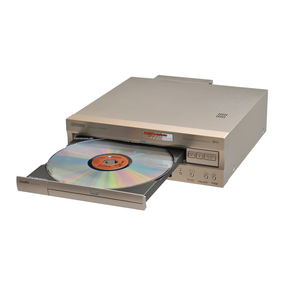
DVL-909
PIONEER ELECTRONIC CORPORATION
PIONEER ELECTRONICS SERVICE, INC. P.O. Box 1760, Long Beach, CA 90801-1760, U.S.A.
PIONEER ELECTRONIC (EUROPE) N.V. Haven 1087, Keetberglaan 1, 9120 Melsele, Belgium
PIONEER ELECTRONICS ASIACENTRE PTE. LTD. 501 Orchard Road, #10-00 Lane Crawford Place, Singapore 0923
c
PIONEER ELECTRONIC CORPORATION 1998
CONTENTS
1. CIRCUIT DESCRIPTION ...................................... 2
FOR DV-S9 AND DV-09 ............................... 10
3. TEST MODE ....................................................... 13
4. IC INFORMATION .............................................. 22
5. FL INFORMATION .............................................. 47
4-1, Meguro 1-Chome, Meguro-ku, Tokyo 153-8654, Japan
SERVICE GUIDE
ORDER NO.
RRV1896
T - IZM APR. 1998 Printed in Japan
Advertisement
Table of Contents

Related Manuals for Pioneer DVL-909


Summary of Contents for Pioneer DVL-909
-
Page 1: Table Of Contents
PIONEER ELECTRONICS SERVICE, INC. P.O. Box 1760, Long Beach, CA 90801-1760, U.S.A. PIONEER ELECTRONIC (EUROPE) N.V. Haven 1087, Keetberglaan 1, 9120 Melsele, Belgium PIONEER ELECTRONICS ASIACENTRE PTE. LTD. 501 Orchard Road, #10-00 Lane Crawford Place, Singapore 0923 PIONEER ELECTRONIC CORPORATION 1998... -
Page 2: Circuit Description
DV-505, DVL-909, DV-S9 1. CIRCUIT DESCRIPTION 1.1 OVERALL BLOCK DIAGRAM DV-505... - Page 3 DV-505, DVL-909, DV-S9 DV-S9 and DV-09...
- Page 4 DV-505, DVL-909, DV-S9 DVL-909 IC601 IC702 PD3381A 4Mbit DRAM HM514800CJ-7 VBR Buffer System CPU IC701 (32bit RISC) PD4833A IC603 IC602 IC604 LSI-11 DRAM I/F FLASH (Bus Arbiter) Sync Demod OEIC SPDL ECC & ID Reg. Motor Program Stream Slider Slider...
- Page 5 DV-505, DVL-909, DV-S9 Sync Tip DVD Y Clamp (IC815 16Mbit SDRAM (from MECHA. CONT. D-EXT ON/OFF IC802 CODE Buffer IC620 (Video, Audio, Sub-picture,GUI) MB811171622A Y OUT D-Extention Pedestal Sync Tip LD Y -100FN LD Y SIGNAL (from MYCB) Circuit Clamp...
- Page 6 DV-505, DVL-909, DV-S9 1.2 EXPLANATION OF EACH MOVEMENT 1.2.1 Sequence Up to Playback DVD SETUP MIRR Modulation Measurement RF AGC ON T Servo ON SLDR Servo ON LD ON Sweep UP Down F Gain Adj. T Gain Adj. Focus Lock AFB Adj.
- Page 7 DV-505, DVL-909, DV-S9 1.2.3 Tracking / Slider Servo ATB: The tracking balance compensation is • TRACKING / SLIDER SERVO achieved by outputting the offset from PICKUP the TBAL output at pin 46 of the digital servo IC, and by biasing the charge pump...
- Page 8 DV-505, DVL-909, DV-S9 1.2.5 Disc Determination Determination is achieved by checking the sine wave by sweeping the lens with the OE IC gain at L and the FSC error amplifier (SGC) Offset compensation at the default setting. If no sine wave is detected, checking is retried after switching the OE IC gain to H and increasing the gain of the FSC error amplifier (SGC).
- Page 9 DV-505, DVL-909, DV-S9 1.2.6 System Control (DVL-909) FLPB, KEYB DVD MAIN IC601 SI1,SO1 PD3381A IC101 SCK1,XRDY PD4890A IC604 IC603 IC602 System Work FLASH Cont. Mode Control 4M ROM (FL Cont.) DATA,ADDRESS IC801 MAIN BUS MB86371 AV-Dec. MAD0–MAD7 Remote Sensor IC701...
-
Page 10: Circuit Descriptions
DV-505, DVL-909, DV-S9 2. CIRCUIT DESCRIPTIONS FOR DV-S9 AND DV-09 2.1 VIDEO SIGNAL PROCESSING BLOCK 2.1.1 PD0259A Block (3) Y/C-timing Adjustment This function changes the output phase of the Y signal with respect The major purposes of the PD0259A block are;... - Page 11 DV-505, DVL-909, DV-S9 2.1.3 Analog Video Signal Processing Block The video signals output from the built-in 10-bit DA converter of the M65677FP pass through a low-pass filter and amplifier, and are output from the DVD MAIN Assy and sent to the VOUT Assy.
- Page 12 DV-505, DVL-909, DV-S9 2.2 DIRB BLOCK (DIRB ASSY) 2.3 96K, 24-Bit, HIBIT LEGATO S (DV-S9 ONLY) SYSTEM (AUDIO ASSY) The two major purposes of the DIRB block are the following: All 16-bit and 20-bit sources are converted to 24-bit data by IC101, (1) Switching between data reproduced from a disc and a data signal which lets a 24-bit data pass through.
-
Page 13: Test Mode
DV-505, DVL-909, DV-S9 3. TEST MODE 3.1 HOW TO ENTER THE TEST MODE (5) Pause 1. It becomes pause condition by pressing [CX] (0E) key of the There is the three following methods in an enters of the test mode. - Page 14 DV-505, DVL-909, DV-S9 (11) Tracking Close (20) Tilt Up 1. Press [STEP RVS] (50) key of the remote control unit in the play A manual moves in the going up direction when [SKIP FWD] (52) condition. key of the remote control unit is pressed during the play at the time 2.
- Page 15 DV-505, DVL-909, DV-S9 3.4 EXPANSION FUNCTION 1 3.5 EXPANSION FUNCTION 2 Set the reception mode of expansion function by pressing [TEST] Set the reception mode of expansion function 2 by pressing [HILITE/ (5E) key of the test mode remote control unit, then expansion function INTRO] (55) key of the remote control unit, then expansion function is able to execute by pressing the key of [0] to [9].
- Page 16 DV-505, DVL-909, DV-S9 Key Name of Mode of Contents of Command Condition Remote Control Unit Remote Control Unit Search address input (A to F) During address input PGM+1 to 6 Search address clear During address input CLEAR A8-45 Escape the search input mode...
- Page 17 DV-505, DVL-909, DV-S9 Special Mention Item (4) If you turn the power on while short-circuiting the short-circuit (1) Indications for the spindle status are as follows: terminal at the side of the system controller, the player will A/B : Spindle accelerator and brake forcibly enter the test mode.
- Page 18 FG servo [FG] 606 : DV-606D, EDU: for education Rough, velocity phase servo [SRV] 909: DVL-909, K88: DVL-K88. Offset addition, rough, velocity phase servo [O_S] Three characters that follow represent the destination code. (7) Mechanism position value [M- ] J : /J, K: /KU, /KC, /KU/KC, RAM: /RAM (China)
-
Page 19: Error Rate
The error rate of CDs can be measured on basic models, such as the DV-505, and that of CDs as well as LDs with sub-Q codes can be measured on DVD/LD-compatible models, such as the DVL-909. The value is displayed in decimal and indicates the number of C1 errors (including the corrected ones) counted during the specified measurement time. - Page 20 DV-505, DVL-909, DV-S9 Using the Function in Test Mode 3.8.3 Startup Sequence This function is not assigned to any remote control keys. Only an open/close operation can trigger the function. The basic flow is shown below. The parentheses indicate a limitation: “base”...
- Page 21 DV-505, DVL-909, DV-S9 3.8.9 PLAY AGC (5) Automatic Sequence Errors (Errors 51 to 55) If any automatic sequence (auto execution command) of the servo Overview DSP is not completed, these errors are generated. The causes differ The SGC voltage is adjusted during playback according to the RF among error numbers.
-
Page 22: Ic Information
DV-505, DVL-909, DV-S9 4. IC INFORMATION • The information shown in the list is basic information and may not correspond exactly to that shown in the schematic diagrams. List of IC PD4890A, PD0260A2, PD0261A2, LA9700M, BA6195FP, LC78650E-P, PD4889A, SRM2B256SLMX70, VYW1536, PD3381A,... - Page 23 DV-505, DVL-909, DV-S9 Pin Function n i l l l o l l o l l o l l o...
- Page 24 DV-505, DVL-909, DV-S9 c t i l l o n i l l l o –...
- Page 25 DV-505, DVL-909, DV-S9 PD0260A2, PD0261A2 (CLDM ASSY : IC101)(DVL-909 ONLY) • Mechanism Control IC Pin Function L " = " " = " L " = " " = " c t i " = " L " = "...
- Page 26 DV-505, DVL-909, DV-S9 c t i t l i t i s L " = " " = " l i h p i l - t l l l o l i h p i l l i h p i l "...
-
Page 27: Block Diagram
DV-505, DVL-909, DV-S9 LA9700M (DVDM ASSY : IC101) • RF IC Block Diagram Scratch Detection PDRF– BPI1 – REFI BPO1 – PDRF BPO2 – BPI2 DLAY1 – – – DLAY2 MIXO1 LDON MIXI1 AGOF MIXI2 PH/RR QAGC MIXO2 –... - Page 28 DV-505, DVL-909, DV-S9 BA6195FP (DVDM ASSY : IC161) • Spindle Driver Block Diagram Driver mute Level shift Pin Function – v i t – v i t...
- Page 29 DV-505, DVL-909, DV-S9 LC78650E-P (DVDM ASSY : IC201)(DVL-909 only) • Servo DSP LSI Block Diagram SLDO Servo TILTE 8bit 8bit SPDO Processor RF_PH (16 16+32 32) TBAL RF_BH TILTDO AUXO JITT VREF Track Counter DVD_CDB PP5/SYNC PP7/EVNT Event Counter LCD Driver...
- Page 30 DV-505, DVL-909, DV-S9 Pin Function t f i l l i l l i t t i y t i t l i a i l t l i...
- Page 31 DV-505, DVL-909, DV-S9 q i l t i r l a i t f i l a i l l i l i f t l i f t l i f t l i f l l i l l i...
- Page 32 DV-505, DVL-909, DV-S9 PD4889A (DVDM ASSY : IC501) • Mechanism Control IC Pin Function " " L c t i " " " r " " " L l l o " " L l l u " " L "...
- Page 33 DV-505, DVL-909, DV-S9 SRM2B256SLMX70 (DVDM ASSY : IC502) • 256 K SRAM (For Mechanism Control IC) Block Diagram Memory-Cell Line Array Decoder 512 64 8 64 8 Row Gate Decoder Control Logic OE, WE Control I/O Buffer Logic 14 18...
- Page 34 DV-505, DVL-909, DV-S9 VYW1536 (DVDM ASSY : IC603)(DV-505 and DVL-909 only) • Flash ROM Block Diagram RY/BY 15-22, 24-31 RY/BY RY/BY BUFFER ERASE INPUT/OUTPUT CIRCUIT BUFFER BYTE CONTROL RESET CIRCUIT WRITE CIRCUIT CHIP ENABLE DATA LATCH OUTPUT ENABLE CIRCUIT Y DECODER...
- Page 35 DV-505, DVL-909, DV-S9 PD3381A (DVDM ASSY : IC601) • System Control CPU Block Diagram 66 65 64 63 62 60 59 58 57 56 55 54 53 51 50 49 48 47 46 45 44 42 41 PORT A ADDRESS...
- Page 36 DV-505, DVL-909, DV-S9 Pin Function l i b l i b l i b...
- Page 37 DV-505, DVL-909, DV-S9 t i r t i r t i r i a l i a l y t i y t i l l i l l i f - r...
- Page 38 DV-505, DVL-909, DV-S9...
- Page 39 DV-505, DVL-909, DV-S9 MB86371 (DVDM ASSY : IC801) • MPEG2 Decoder LSI For DVD Block Diagram Exclusive 16Mbit Parallel port SDRAM Input Signal Memory System Interface Decoder Block Controller Block Internal Video Sub- Sync. Decoder picture Control Block Block Starting...
- Page 40 DV-505, DVL-909, DV-S9 Pin Function " ( : " L " : " i g i i g i i g i i g i ) t i i g i - t l ) t i - t l...
- Page 41 DV-505, DVL-909, DV-S9 t l i f t l i f t l i f , y l o " . " , y l o " . " l e l l e l l e l " "...
- Page 42 DV-505, DVL-909, DV-S9 " " L y l l...
- Page 43 DV-505, DVL-909, DV-S9 MB811171622A-100FN (DVDM ASSY : IC802) • Code Buffer (16M bit SDRAM) Block Diagram Clock Bank 1 Blocks Buffer Bank 0 Control Command Signal Decoder Latch DRAM Core Mode (2,048 256 16) Address Register Buffer/ Register & Bank...
- Page 44 DV-505, DVL-909, DV-S9 CY2081SL-611 (DVDM ASSY : IC813) • Clock Generate IC Block Diagram XTALIN Refference CLKA PLL1 EPROM- Oscillator XTALOUT Configurable Multiplexer PLL2 CLKB Drive Logic PLL3 CLKC OE/PD/FS/SUSPEND Pin Function v i t v i t v i t...
- Page 45 DV-505, DVL-909, DV-S9 PD2058A ( DVDM ASSY : IC901 )(DV-505 and DVL-909 only) • Digital Signal Processor For Audio Block Diagram 1–3,6–11, 5,14,34,52 42–44 13 12 4,31 53–60 Offset RAM Coefficient Coefficient Data RAM 64w 16b 128w 24b Delay RAM...
- Page 46 DV-505, DVL-909, DV-S9 l a i n i l l a i n i l t f i t f i " " 0 y t i n i l l l i l l i l l i c t i...
-
Page 47: Fl Information
DV-505, DVL-909, DV-S9 5. FL INFORMATION VAW1046 (FLKB ASSY : V101)(DV-505 and DVL-909 only) • FL DISPLAY DOLBY 96kHz ANGLE LAST MEMO CONDITION DIGITAL TITLE CHP / TRK REMAIN TOTAL • ANODE AND GRID ASSIGNMENT ANGLE TITLE LAST MEMO CONDITION...
Need help?
Do you have a question about the DVL-909 and is the answer not in the manual?
Questions and answers