
Related Manuals for Bose 2150


Summary of Contents for Bose 2150
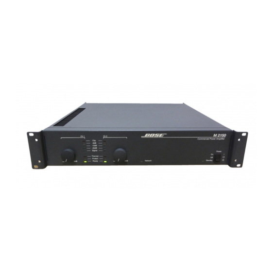
- Page 1 Model 2150 Commercial Power Amplifier Service Manual ©2008 Bose Corporation Part Number 216306 Rev. 01...
-
Page 2: Table Of Contents
Packaging Part List, Model 2150 Amplifier ..................6 Part List Notes ..........................7 Main Part List, Model 2150 Amplifier (items not shown on a part drawing) ........ 7 Main Part List (Continued), Model 2150 Amplifier (see Figure 1) ..........8 Figure 1. -
Page 3: Safety Information
• Transport or store ESDS devices in ESD protective bags, bins, or totes. Do not insert unprotected devices into materials such as plastic, polystyrene foam, clear plastic bags, bubble wrap or plastic trays. WARRANTY The Bose ® Model 2150 amplifier is covered by a five-year, transferable, limited warranty. -
Page 4: Specifications
> 95 dB, A-Weighted below full bandwidth power Channel Separation: > 80 dB at 1 kHz ® CMRR: > 80 dB at 1 kHz (without Bose input module) Slew Rate: > 10V/uSec Sensitivity: 0.775 Vrms for rated power at 1 kHz... - Page 5 • Speaker Output via large gauge Euro style connectors (accepts 12 gauge wire) • Power Switch, 3 positions, On, Off and Standby • AC Line Cord (Detachable IEC Type) • Optional Accessories: - Computer Control and Monitoring via Bose ACM-1 amplifier control module Physical Characteristics: Cooling Method: Convection...
-
Page 6: Amplifier/Driver Board Version Information
8100.0218 262210 EURO Model 2060/2150 Manual, Owners, EN/ FR/ SP, Model 8100.0219 262194 US/CSA 2060/2150 /EURO/ UK/AUS Declaration of Conformity, Bose 2150 8110.0012A 262318 EURO amplifier Line Cord, 120V, S250AH 4150.0009 262099 US/CSA Line Cord, MOD, 3x1.0mm, 10A, 4150.0015 262117 250V Line Cord, MOD, 3x1.0mm, 13A,... -
Page 7: Part List Notes
4. This part is referenced for informational purposes only. It is not stocked as a repair part. MAIN PART LIST Model 2150 Amplifier (items not shown on a part drawing) ® ® ® ® Item Description Vendor Part Qty. -
Page 8: Main Part List (Continued), Model 2150 Amplifier (See Figure 1)
32x3/8 Screw, TF, 6-32x1/4, FHP, UC, ST, 5113.0037 262113 Screw, TF, 4-40x1/4, FHP, UC, ST, 5112.0026 199771 Cover, 2U, Bose 2060/2150 700487.30 262102 Amplifier Chassis Assembly (refer to Figure 2) Figure 1. Model 2150 Amplifier Top Cover Removal Exploded View... -
Page 9: Main Part List (Continued), Model 2150 Amplifier (See Figure 2)
MAIN PART LIST (CONTINUED) Model 2150 Amplifier (see Figure 2) ® ® ® ® Item Description Vendor Part Qty. Note Bose Part Number Number Number Screw, TF, 6-32x1/4, FHP, UC, ST, 5113.0037 262113 Amplifier Assembly (refer to Figure 6) Nut, Mini STZ, 4-40... - Page 10 Figure 2. Model 2150 Amplifier Internal Assemblies Exploded View...
-
Page 11: Main Part List (Continued), Model 2150 Amplifier (See Figure 3)
262090 Chassis, Shield, Amp, CV (bottom) 700508 262091 Signal Processor PCB Assembly 9000.0447.03 262087 Screw, TF, SEMS, 4-40x3/8, HWH, 5112.0034 262111 ST, BZ Screw, TF, SEMS, 4-40x1/2, HWH, 5112.0031 262110 ST, BZ Figure 3. Model 2150 Amplifier Module Exploded View... -
Page 12: Electrical Part Lists
ELECTRICAL PART LIST Input Module Assembly Resistors ® ® ® ® Reference Description Vendor Part Note Bose Part Designator Number Number 332k, MF, 1/4W, 1% 1226.3323 183000 332k, MF, 1/4W, 1% 1226.3323 183000 332k, MF, 1/4W, 1% 1226.3323 183000 332k, MF, 1/4W, 1% 1226.3323... - Page 13 .01uF, CRML, Rdl, 100V, +80/-20% 201-00068-00 182780 .01uF, CRML, Rdl, 100V, +80/-20% 201-00068-00 182780 .001uF, PE, RDL, 100V, 10% 2458.0102 182839 Diodes Reference Description Vendor Part Bose Part Note Designator Number Number 1N4004, 400V 3100.0017 182811 1N4148 3100.0004 182868 1N4148 3100.0004...
- Page 14 3200.0026 182874 PNP, MPSA56, TO-92 3200.0003 182875 PNP, MPSA56, TO-92 3200.0003 182875 Integrated Circuits Reference Description Vendor Part Bose Part Note Designator Number Number Balanced Line Receiver, SSM2141 3510.2141 183005 Balanced Line Receiver, SSM2141 3510.2141 183005 OP-AMP W/Switch, NJM2120L 330-30062-01...
-
Page 15: Barrier Pcb Assembly (Part Of Input Module Assembly)
ELECTRICAL PART LIST Barrier PCB Assembly (part of Input Module Assembly) ® ® ® ® Reference Description Vendor Part Note Bose Part Designator Number Number Harness, Conn, 2 Position, 22 AWG, 550-10083-01 262121 3.5 in. Harness, Conn, 2 Position, 22 AWG,... -
Page 16: Amplifier Pcb Assembly (Board Part Number 6000.0435)
ELECTRICAL PART LIST Amplifier PCB Assembly (board part number 6000.0435) Resistors ® ® ® ® Reference Description Vendor Part Note Bose Part Designator Number Number RT600 Thermistor, PTC, 2.2k 1200.0001 262126 R600 2.7k, CF, 1/8W, 5% 1124.0272 R601 10 Ohm, MF, 1/4W, 5% 1204.0100... - Page 17 0 Ohm, 1/8W 1124.0000 R658 0 Ohm, 1/8W 1124.0000 R659 0 Ohm, 1/8W 1124.0000 Capacitors Reference Description Vendor Part Bose Part Note Designator Number Number C601 100pF, Cer Disc, NPO, 100V, 5% 2174.0101 C602 100pF, Cer Disc, NPO, 100V, 5% 2174.0101 C603 100pF, Cer Disc, NPO, 100V, 5% 2174.0101...
- Page 18 ELECTRICAL PART LIST Amplifier PCB Assembly (board part number 6000.0435) Capacitors (continued) ® ® ® ® Reference Description Vendor Part Note Bose Part Designator Number Number C630 .1uF, CRML, X7R, 100V, 5mm, 20% 2175.0104 199761 C631 100uF, AE, RDL, 100V, 20% 2936.0107...
- Page 19 401-30015-01 262130 L620 11uH, 9A, Filter 4500.0032 262129 L621 Jumper, 18 AWG, .5 inch, Insulated 401-30015-01 262130 Diodes Reference Description Vendor Part Bose Part Note Designator Number Number D600 1N4002 3100.0005 262192 D601 1N4002 3100.0005 262192 D602 1N5263B, Zener, 56V, .5W, 5% 3110.3630...
- Page 20 ELECTRICAL PART LIST Amplifier PCB Assembly (board part number 6000.0435) Miscellaneous ® ® ® ® Reference Description Vendor Part Note Bose Part Designator Number Number J601 Cable, IDC, PCB/PLG, 10 Cond, 4 in 4148.0018 262139 J602 Cable, IDC, PCB/PLG, 10 Cond, 4 in 4148.0018...
-
Page 21: Amplifier Pcb Assembly (Board Part Number 8005.0587)
ELECTRICAL PART LIST Amplifier PCB Assembly (board part number 8005.0587) Resistors ® Reference Description Bose Part Vendor Part Note Designator Number Number R602 93.1K, MF, 1/8W, 1% 1126.9312 R603 93.1K, MF, 1/8W, 1% 1126.9312 R604 1.00 MEG, MF, 1/8W, 1% 1126.1004... - Page 22 27 OHM, MOF, 2W, 5% 1544.0270 R666 16 OHM, MOF, 1W, 5% L.1444.0160 R667 16 OHM, MOF, 1W, 5% L.1444.0160 Capacitors Reference Description Bose Part Vendor Part Note Designator Number Number C600 220pF, CD, 10%, 1000V L.201-00018-00 C601 0.01uF, CD, 20%, 500V L.201-00034-00...
- Page 23 ELECTRICAL PART LIST Amplifier PCB Assembly (board part number 8005.0587) Capacitors (continued) ® Reference Description Bose Part Vendor Part Note Designator Number Number C620 0.47uF, CRML, 20%, Z5U, 50V L.2175.0474 C621 100pF, CD, 5%, NPO, 100V 2174.0101 C622 0.47uF, CRML, 20%, Z5U, 50V L.2175.0474...
- Page 24 0.01uF, CD, 20%, 500V L.201-00034-00 C685 0.18uF, MPP, HF, 5%, 250V L.2594.0184 C686 0.18uF, MPP, HF, 5%, 250V L.2594.0184 Inductors Reference Description Bose Part Vendor Part Note Designator Number Number L610 INDUCTOR, FILTER, 11uH, 9A L.4500.0032 L611 INDUCTOR, IRON, PWDR, 7.8uH, 4500.0054...
- Page 25 SWITCHING, MUR120, AXL L.3100.0001 D621 SWITCHING, MUR120, AXL L.3100.0001 D624 SWITCHING, MUR120, AXL L.3100.0001 D625 SWITCHING, MUR120, AXL L.3100.0001 Transistors Reference Description Bose Part Vendor Part Note Designator Number Number Q601 PNP, 2N4403TO-92 262134 3200.0002 Q610 N-CH FET, STW34NB20, TO-247 L.3210.0017 Q611 N-CH FET, STW34NB20, TO-247 L.3210.0017...
- Page 26 ELECTRICAL PART LIST Amplifier PCB Assembly (board part number 8005.0587) Miscellaneous ® Reference Description Bose Part Vendor Part Note Designator Number Number GROMMET, 1/4 ID x 9/16 OD 5820.0007 GROMMET, 1/4 ID x 9/16 OD 5820.0007 GROMMET, 1/4 ID x 9/16 OD 5820.0007...
-
Page 27: Power Supply Pcb Assembly
R402 4.7k, MOF, 2W, 5% 1544.0472 262299 R403 2.2k, MOF, 1W, 5% 1444.0222 262296 Capacitors Reference Description Vendor Part Bose Part Note Designator Number Number C400 .1uF, MPE, 250V, 10% 2462.0104 C401 .1uF, MPE, 250V, 10% 2462.0104 C402 .1uF, MPE, 250V, 10% 2462.0104... - Page 28 3100.0017 182811 D414 1N4004, 400V 3100.0017 182811 D415 1N4004, 400V 3100.0017 182811 Integrated Circuits Reference Description Vendor Part Bose Part Note Designator Number Number U400 VOLT REG, +15V, NJM7815FA 3430.0005 262146 U401 VOLT REG, -15V, 7915 3430.0006 262147 U402 VOLT REG, -15V, 7915 3430.0006...
- Page 29 ELECTRICAL PART LIST Power Supply PCB Assembly Miscellaneous ® ® ® ® Reference Description Vendor Part Note Bose Part Designator Number Number WL400 Terminal, Quick-Connect, .250 TAB 4200.0017 262148 WL401 Terminal, Quick-Connect, .250 TAB 4200.0017 262148 WL402 Terminal, Quick-Connect, .250 TAB 4200.0017...
-
Page 30: Switch Pcb Assembly
Number R100 33k, MOF, 1W, 5% 1444.0333 262297 R101 33k, MOF, 1W, 5% 1444.0333 262297 Capacitors Reference Description Vendor Part Bose Part Note Designator Number Number .01uF, Cer Disc, 250VAC, 10%, 201-00035-00 3, 4 UL/CSA Diodes Reference Description Vendor Part... - Page 31 18 Ohm, HM, CC, 1/2W, 5% 1354.0180 187934- 18R0 R103 8.2 Ohm, CF, 1/2W, 5% 1324.0829 182857 Capacitors Reference Description Vendor Part Bose Part Note Designator Number Number C100 .10uF, MP, 250VAC, UL/CSA 2462.1104 182846 C101 .10uF, MP, 250VAC, UL/CSA 2462.1104...
-
Page 32: Ac Input/Output Pcb Assembly
ELECTRICAL PART LIST AC Input/Output PCB Assembly Miscellaneous (continued) ® ® ® ® Reference Description Vendor Part Note Bose Part Designator Number Number WL100 Terminal, Quick-Connect, .250 Tab 4200.0017 262148 WL101 Terminal, Quick-Connect, .250 Tab 4200.0017 262148 WL102 Terminal, Quick-Connect, .250 Tab 4200.0017... -
Page 33: Interface Pcb Assembly
1124.0271 R818 68k, CF, 1/4W, 5% 1224.0683 R819 150k, CF, 1/8W, 5% 1124.0154 Capacitors Reference Description Vendor Part Bose Part Note Designator Number Number C801 330pF, Cer Disc, COG, 100V, 5% 2174.0331 182992 C802 330pF, Cer Disc, COG, 100V, 5% 2174.0331... - Page 34 D805 1N4148 3100.0004 182868 D806 1N4148 3100.0004 182868 D807 1N4148 3100.0004 182868 Transistors Reference Description Vendor Part Bose Part Note Designator Number Number Q801 PNP, 2N4403, TO-92 3200.0002 262134 Q802 NPN, 2N4401, TO-92 3200.0001 262168 Q803 PNP, 2N4403, TO-92 3200.0002...
-
Page 35: Digital Signal Processor (Dsp) Pcb Assembly
ELECTRICAL PART LIST Digital Signal Processor (DSP) PCB Assembly Resistors ® ® ® ® Reference Description Vendor Part Note Bose Part Designator Number Number RN500 22k, RES NET x8, 16 Pin, DIP, 2% 1095.1223 262174 Pot, Trim, 50k, 6mm, PC Mnt 4410.0017... - Page 36 ELECTRICAL PART LIST Digital Signal Processor (DSP) PCB Assembly Resistors (continued) ® ® ® ® Reference Description Vendor Part Note Bose Part Designator Number Number R464 10k, CF, 1/8W, 5% 1124.0103 R465 13.0k, MF, 1/8W, 1% 1126.1302 R466 4.99k, MF, 1/8W, 1% 1126.4991...
- Page 37 ELECTRICAL PART LIST Digital Signal Processor (DSP) PCB Assembly Resistors (continued) ® ® ® ® Reference Description Vendor Part Note Bose Part Designator Number Number R523 2.21k, MF, 1/8W, 1% 1126.2211 R524 1k, CF, 1/8W, 5% 1124.0102 R525 2.21k, MF, 1/8W, 1% 1126.2211...
- Page 38 ELECTRICAL PART LIST Digital Signal Processor (DSP) PCB Assembly Resistors (continued) ® ® ® ® Reference Description Vendor Part Note Bose Part Designator Number Number R569 10.0k, MF, 1/8W, 1% 1126.1002 R570 10.0k, MF, 1/8W, 1% 1126.1002 R571 121 Ohm, MF, 1/8W, 1% 1126.1210...
- Page 39 ELECTRICAL PART LIST Digital Signal Processor (DSP) PCB Assembly Capacitors ® ® ® ® Reference Description Vendor Part Note Bose Part Designator Number Number C428 1uF, AE, RDL, 50V, 20% 2930.0105 C431 .1uF, MPE, 50V, 5% 2452.0104 C432 100uF, AE, RDL, 25V, 20% 2930.0107...
- Page 40 ELECTRICAL PART LIST Digital Signal Processor (DSP) PCB Assembly Capacitors (continued) ® ® ® ® Reference Description Vendor Part Note Bose Part Designator Number Number C533 .1uF, MPE, 50V, 5% 2452.0104 C534 .1uF, MPE, 50V, 5% 2452.0104 C535 .1uF, MPE, 50V, 5% 2452.0104...
- Page 41 330pF, Cer Disc, COG, 100V, 5% 2174.0331 182992 C587 10uF, AE, RDL, 35V, 20% 2930.0106 C588 10uF, AE, RDL, 35V, 20% 2930.0106 Diodes Reference Description Vendor Part Bose Part Note Designator Number Number D425 1N4148 3100.0004 182868 D426 1N4148 3100.0004 182868...
- Page 42 3200.0001 262168 Q500 NPN, 2N4401, TO-92 3200.0001 262168 Q501 NPN, 2N4401, TO-92 3200.0001 262168 Integrated Circuits Reference Description Vendor Part Bose Part Note Designator Number Number U425 COMPARATOR, QUAD, LM339 3410.0339 262177 U426 COMPARATOR, QUAD, LM339 3410.0339 262177 U427 COMPARATOR, QUAD, LM339 3410.0339...
- Page 43 ELECTRICAL PART LIST Digital Signal Processor (DSP) PCB Assembly Miscellaneous ® ® ® ® Reference Description Vendor Part Note Bose Part Designator Number Number J101 Conn, Hdr, Shrd, 10x2, .1 Pol. 4205.0022 262185 J401 Conn, Hdr, .1 CTR, 3 Pin, Gold 4205.0003...
-
Page 44: Display Pcb Assembly
R716 7.5k, CF, 1/4W, 5% 1224.0752 182953 R717 7.5k, CF, 1/4W, 5% 1224.0752 182953 Capacitors Reference Description Vendor Part Bose Part Note Designator Number Number C700 1uF, AE, RDL, 50V, 20% 2930.0105 C701 1uF, AE, RDL, 50V, 20% 2930.0105 C703 10uF, AE, RDL, 35V, 20% 2930.0106... - Page 45 LED, RECT, 2x5mm, YELLOW 3600.0025 262158 D719 1N4148 3100.0004 182868 D720 1N4148 3100.0004 182868 Integrated Circuits Reference Description Vendor Part Bose Part Note Designator Number Number U700 OP-AMP, DUAL, BA4560 3410.4560 262179 U701 OP-AMP, DUAL, BA4560 3410.4560 262179 U702 OP-AMP, DUAL, BA4560 3410.4560...
-
Page 46: Disassembly Procedures
DISASSEMBLY PROCEDURES Note: Refer to Figure 1 for the following 3.4 Unplug the ribbon cable that runs from procedures. the interface board (12) to the amplifier module at J800. 1. Top Cover Removal 3.5 Unplug the ribbon cable that runs from 1.1 Remove the three screws (3) that secure the power supply board (25) to the signal the rack-mount ears (2) to the amplifier... - Page 47 DISASSEMBLY PROCEDURES 4.4 Unplug the ribbon cable that runs from 5.5 Remove the screws (9) that secure the the Interface board (12) at the rear of the output devices and thermistor RT600 to the amplifier chassis (23) to the processor board heatsink.
- Page 48 DISASSEMBLY PROCEDURES 7.5 Remove the six screws (11) that secure 9. Line Filter Removal the AC Input/Output board to the standoffs (14). Lift the board out of the amplifier chas- 9.1 Perform procedure 7. sis (23). Note: It's not necessary to remove all of the wires on the AC Input/Output board 8.
- Page 49 Note: There are two CV (constant voltage) switch (24). audio output transformers used in the Model 2150 amplifier; one for each channel. The 14.3 Using a flat-blade screwdriver, press in transformer closest to the side of the ampli- the tabs on the top and bottom of the AC...
-
Page 50: Test Procedures
TEST PROCEDURES Figure 4. Model 2150 amplifier rear panel Note: Refer to figures 4 and 5 for the follow- ing tests. Refer to the Model 2150 amplifier owner's guide for additional operational and Signal Generator hookup information. outputs Equipment Required: •... - Page 51 TEST PROCEDURES 2. Signal Processor PCB Gain Test 3. Frequency Response Test 2.1 Remove the amplifier top cover using 3.1 On the front panel of the amplifier, set disassembly/assembly procedure 1. the gain controls fully CW. On the rear panel, set the configuration dip switches (7) OFF CAUTION: Components with dangerous (down).
- Page 52 TEST PROCEDURES 4.6 Measure the distortion level at the left 6.4 Using a DMM, check the FX SEND channel output. Harmonic distortion should terminals for a 100 mV + 2.6 mV output level. be < 0.5% (20 Hz to 20 kHz bandwidth). 6.5 Jumper the SEND outputs into the 4.7 Repeat steps 4.2 through 4.6 for the RECV inputs.
- Page 53 TEST PROCEDURES 8.3 Apply a 775 mVrms, 1 kHz signal to the 10.2 Connect a dB meter to the amplifier left left channel inputs. Reference a dB meter to channel 4 Ohm outputs. Bandwidth limit the the left channel outputs. This is the 0 dB measurement to 20 kHz and apply an A- reference level.
- Page 54 TEST PROCEDURES 12.4 Use a 0.1 Ohm, 2 Watt (or greater) 14.5 Verify that the amplifier powers up resistor to short across the left amplifier normally. channel's 4 Ohm load resistor. Verify that the amplifier output mutes, the amplifer 14.6 Use a DC voltmeter to measure the resets and attempts to turn on after a short voltage at the sequence connector SEND delay but continues to cycle as long as the...
- Page 55 SEND RECV IN FX IN FX ON CLIP ON HP ON HP 80Hz 120Hz 120Hz IN FX ON CLIP ON HP 80Hz 120Hz Figure 6. Model 2150 Amplifier Signal Flow Block Diagram...
-
Page 56: Theory Of Operation
The Model 2150 is rated at 150 Watts per channel into 4 Ohms, 8 Ohms, 25V, 35V, 50V, 70V or 100V. In bridged-mono operation, it is rated at 300 Watts. - Page 57 Note: Some amplifiers will be equipped with the Bose ACM-1 Amplifier Control Module in place of the standard Bose Input Module. This module retains all of the capabilities of the Bose Input Module, except sequence, and includes the ability to control and monitor the amplifier over a control network.
- Page 58 THEORY OF OPERATION Input Module (continued) The signal inputs are designed for balanced connection, though unbalanced inputs can be configured by proper input wiring. Channel 1 (CH1) line-level inputs are made via P4 [A3] and J4 [A4], Channel 2 (CH2) input connections are made via P1 [A1] and J5 [A2]. P4 and P1 allow for the insertion of either male XLR or phone plugs.
- Page 59 THEORY OF OPERATION Input Module (continued) In DUAL MONO mode both amplifier channels are driven by the signal applied to the CH2 input. U6-1 is driven high (+15V) and U5-1 is driven low (+7.5V), selecting CH2 to drive both channels of the amplifier.
- Page 60 THEORY OF OPERATION Signal Processing (continued) Linear regulators U510 [F3] and U513 [H3] provide separate 5V reference voltages to the Master Level and Remote Level control circuits. Master Level potentiometer RT710 [Display PCB, B1] operates as a voltage divider between signal ground (CW setting) and reference 5V (CCW setting) producing a master level control voltage at RT710 wiper varying linearly from 0 to 5V.
- Page 61 THEORY OF OPERATION Signal Processing (continued) Limiter operation can be disabled through the ACM-1 control interface by pulling J101p17 [Signal Processor sheet2, B5] to ground. Q427 [E3] also turns on when clip detector output U427p2 is pulled up, sinking current through limiting resistor R441 lighting “Clip” LED D715 [Display PCB, D3] (J700p14 Signal Processor Assy to P700p14 Display Assy).
- Page 62 THEORY OF OPERATION Power Amplifier PCB (continued) Two circuits provide power to the digital amplifier driver. Linear regulator U602 [C2] supplies 5V for internal processor power. Buck switching converter U600 [B1] operates between power ground and the negative rail, generating VS -referenced 12V power supply VN12REF, used by the driver for low-side output FET gate drive.
- Page 63 THEORY OF OPERATION Power Amplifier PCB (continued) At approximately 90°C, the thermistor voltage at U425Ap4 exceeds the threshold at U425Ap5 and output U425Ap2 pulls to ground. Threshold voltage at U425Ap5 drops as the divider is re- biased through R435 and D428, providing thermal hysteresis of ~5°C. The amplifier turns off when C432 is discharged through D429, and “Thermal”...
- Page 64 THEORY OF OPERATION Display PCB (continued) The “-20dB”, “-12db”, and “-6dB” LEDs are driven by circuitry that samples the power amplifier output. Due to the function of the output transformer, power amplifier output level of 25V corre- sponds to rated output power. Signal is taken from output side of R646 via fuse resistor R650 and fed to the signal processor assembly (J601p2 Power Amp Assy to J601p2 Signal Processor Assy) where R427, R428 attenuate the signal to levels compatible with op amp inputs and R427, C586 form a low pass network rejecting RF noise.
- Page 65 THEORY OF OPERATION Display PCB (continued) Current overload or over-/ under-voltage events in the power amplifier trigger a protection control cycle. During this timeout, Q433 [Signal Processor sheet2, G2] turns on, sinking current through limiting resistor R460 lighting “Protect” LED D713 [Display PCB, D3] (J700p19 Signal Processor Assy to P700p19 Display Assy).
-
Page 66: Circuit Board Layout Diagrams
AC Input / Output PCB Top Etch Layout AC Input / Output PCB Bottom Etch Layout Switch PCB Top Etch Layout Switch PCB Bottom Etch Layout... - Page 67 Amplifier PCB, 6000.0435 Version, Top Etch Layout...
- Page 68 Amplifier PCB, 6000.0435 Version, Bottom Etch Layout...
- Page 69 Amplifier PCB, 8005.0587 Version, Top Component Layout...
- Page 70 Display PCB Top Etch Layout Display PCB Bottom Etch Layout Interface PCB Top Etch Layout Interface PCB Bottom Etch Layout...
- Page 71 Power Supply PCB Top Etch Layout Power Supply PCB Bottom Etch Layout...
- Page 72 Signal Processor PCB Top Etch Layout...
- Page 73 Signal Processor PCB Bottom Etch Layout...
-
Page 74: Integrated Circuit Diagrams
INTEGRATED CIRCUIT DIAGRAMS Pin Function 1. A Output 2. A Inverting Input 3. A Non-inverting Input 4. VEE 5. B Non-inverting Input 6. B Inverting Input 7. B Output 8. VCC 2SC4793 power transistor BA4560 dual op-amp BTA41 triac KA339 quad differential comparator Pin Function IC, Volt Reg, 1. - Page 75 INTEGRATED CIRCUIT DIAGRAMS Pin Function 1. Output1 2. Inverting input1 1. OUT 1 3. Non-inverting input 1 2. IN 1 (-) 4. -Vcc 3. IN 1 (+) 5. Non-inverting input 2 4. GND 6. Inverting input 2 5. IN 2 (+) 7.
- Page 76 INTEGRATED CIRCUIT DIAGRAMS 1. Reference 25k Ohm 2. Inverting input 3. Non-inverting input 25k Ohm 4. -Vcc 5. Sense 25k Ohm 6. Output 7. +Vcc 8. NC 25k Ohm PS7341-1A solid state relay SSM2141 differential line receiver Cathode Identifier STW34NB20 N channel MOSFET VTL5C4 triac THAT 2150A Voltage Controlled Amplifier equivalent circuit...
- Page 77 INTEGRATED CIRCUIT DIAGRAMS THAT 2150A Voltage Controlled Amplifier typical circuit TAO103A amplifier simplified circuit...
- Page 78 INTEGRATED CIRCUIT DIAGRAMS Function Description AGND Analog ground OVERLOADB Logic output. When low, indicates that the level of the input signal has overloaded the amplifier. Positive 5 Volts. MUTE Logic input. When high, both amplifiers are muted. When low (grounded), both amplifiers are fully operational. 5, 6 IN2, IN1 Single-ended input (channel 1 and 2).
-
Page 79: Troubleshooting
Troubleshooting Problem What to do • No sound, no power Check to see if amplifier power is off. Turn on. (usually indicates a power • Line cord disconnected. supply problem, either in • Poor fit between the plug and AC receptacle. Try another the power line or the receptacle. -
Page 80: Service Manual Revision History
SERVICE MANUAL REVISION HISTORY Date Revision Description of Change Change Driven Pages Level Affected 1/01 Document released at revision 00. Service manual initial release 8/08 New revision amplifier board info added. New board 21-26... - Page 81 SPECIFICATIONS AND FEATURES SUBJECT TO CHANGE WITHOUT NOTICE Bose Corporation The Mountain Framingham Massachusetts USA 01701 P/N: 216306 Rev. 01 8/2008 (P) FOR TECHNICAL ASSISTANCE OR PART ORDERS, CALL 1-800-233-4408 http://serviceops.bose.com...
Need help?
Do you have a question about the 2150 and is the answer not in the manual?
Questions and answers