Table of Contents
Advertisement
Quick Links
This document outlines the basic steps and functions that are required to ensure the proper operation of
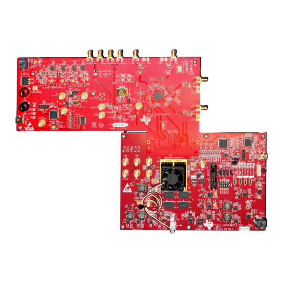
the Texas Instruments (TI) ADS54J54 Evaluation Module (EVM). The EVM includes an ADS54J54EVM, a
cable for connection to an external 5-VDC power supply, and a mini-USB cable. This EVM is designed to
be used with the TI TSW14J56EVM JESD204B capture card using an FMC connector interface or FPGA
development boards, such as the Xilinx KC705 or Altera Arria V. The ADS54J54EVM contains an
ADS54J54 (14-bit) four-channel, 500-MSPS ADC. The EVM also contains a TI LMK04828 clock jitter
cleaner. When used with the TSW14J56EVM, JESD204B standard output data from the EVM is captured
and sent to a host PC for analysis. This guide helps users to quickly evaluate the performance of the
ADS54J54EVM board by capturing and displaying waveforms using the TSW14J56 with the High Speed
Data Converter Pro GUI software. The EVM schematics, BOMs, and layout files are found in the design
package under the ADS54J54EVM tool folder on www.ti.com.
...................................................................................................................
1
1.1
1.2
2
2.1
2.2
3
3.1
3.2
3.3
1
2
3
4
5
6
7
8
9
...................................................................................................................
10
11
1
2
Microsoft, Windows are registered trademarks of Microsoft Corporation.
SLAU616A - January 2015 - Revised January 2016
Submit Documentation Feedback
.............................................................................................................
.......................................................................................................
.............................................................................................................
.............................................................................................
.................................................................................................
...........................................................................................................
...............................................................................................
............................................................................................
List of Figures
....................................................................................
....................................................................................................
..............................................................................................
.......................................................................................
.....................................................................................
...........................................................................................
.....................................................................................
...................................................................................................
List of Tables
....................................................................................
Copyright © 2015-2016, Texas Instruments Incorporated
SLAU616A - January 2015 - Revised January 2016
ADS54J54 Evaluation Module
Contents
........................................................................
..............................................................
......................................................
User's Guide
.....................................
ADS54J54 Evaluation Module
2
2
2
4
4
4
14
14
15
15
2
5
6
8
9
10
11
12
13
14
17
3
6
1
Advertisement
Table of Contents

Related Manuals for Texas Instruments ADS54J54EVM


Summary of Contents for Texas Instruments ADS54J54EVM
-
Page 1: Table Of Contents
TI TSW14J56EVM JESD204B capture card using an FMC connector interface or FPGA development boards, such as the Xilinx KC705 or Altera Arria V. The ADS54J54EVM contains an ADS54J54 (14-bit) four-channel, 500-MSPS ADC. The EVM also contains a TI LMK04828 clock jitter cleaner. -
Page 2: Introduction
Introduction Overview The ADS54J54EVM is an evaluation module (EVM) used to evaluate Texas Instruments’ ADS54J54 ADC and the LMK04828 clock jitter cleaner devices. The ADS54J54 (14-bit) is a four-channel, 500-MSPS ADC with buffered analog inputs and outputs featuring a JESD204B interface. The EVM has transformer- coupled analog inputs accommodating a wide range of signal sources and frequencies. -
Page 3: Input And Output Connectors And Jumper Descriptions Of The Ads54J54Evm
U11 enable. Install jumper to disable switcher U11. Default is uninstalled. JP1 (PWRGD) Test point for power good output pin from U11. SLAU616A – January 2015 – Revised January 2016 ADS54J54 Evaluation Module Submit Documentation Feedback Copyright © 2015–2016, Texas Instruments Incorporated... -
Page 4: Software Control
3. Run setup.exe and follow the installation prompts. 4. Start the GUI by going to Start Menu → All Programs → Texas Instruments ADCs → ADS54J54 EVM GUI. 5. When plugging the board into the computer for the first time through the USB cable, you are prompted to install the USB drivers. -
Page 5: Top-Level Block Diagram Window Of The Ads54J54 Gui
EVM at any time, a reset for each device is required. Figure 2. Top-Level Block Diagram Window of the ADS54J54 GUI SLAU616A – January 2015 – Revised January 2016 ADS54J54 Evaluation Module Submit Documentation Feedback Copyright © 2015–2016, Texas Instruments Incorporated... -
Page 6: Ads54J54 Controls Tab
Sets how close to full scale the input can be before the fast overrange will detect overrange OVRx OUT EN Selects the function of the fast OVR pin for each of the four channels ADS54J54 Evaluation Module SLAU616A – January 2015 – Revised January 2016 Submit Documentation Feedback Copyright © 2015–2016, Texas Instruments Incorporated... - Page 7 Selects the length of the PRBS test pattern PRBS Enable Selects the PRBS test pattern to be output on individual serial lane outputs SLAU616A – January 2015 – Revised January 2016 ADS54J54 Evaluation Module Submit Documentation Feedback Copyright © 2015–2016, Texas Instruments Incorporated...
-
Page 8: Jesd204B Configuration Tab
FPGA receiving JESD204B serial sample data from the EVM) must be configured with the same parameters as the ADS54J54. Figure 4. JESD204B Configuration Tab ADS54J54 Evaluation Module SLAU616A – January 2015 – Revised January 2016 Submit Documentation Feedback Copyright © 2015–2016, Texas Instruments Incorporated... -
Page 9: Lmk04828 Pll1 Configuration Tab
Consult the LMK04828 data sheet (SNAS605) and design tools for more information regarding the proper settings for configuring PLL1, particularly for the proper settings for the PLL1 phase detector and charge pump values. SLAU616A – January 2015 – Revised January 2016 ADS54J54 Evaluation Module Submit Documentation Feedback Copyright © 2015–2016, Texas Instruments Incorporated... -
Page 10: Lmk04828 Pll2 Configuration Tab
LMK04828 datasheet is indispensable in understanding the function of each of these many controls and how these controls should be set for a specific use of the EVM. Figure 6. LMK04828 PLL2 Configuration Tab ADS54J54 Evaluation Module SLAU616A – January 2015 – Revised January 2016 Submit Documentation Feedback Copyright © 2015–2016, Texas Instruments Incorporated... -
Page 11: Lmk04828 Clock Outputs Tab
12 to generate a 250-MHz DCLK to the FMC connector. These two divider ratios can be seen in Figure Figure 7. LMK04828 Clock Outputs Tab SLAU616A – January 2015 – Revised January 2016 ADS54J54 Evaluation Module Submit Documentation Feedback Copyright © 2015–2016, Texas Instruments Incorporated... -
Page 12: Lmk04828 Sysref And Sync Tab
7 SYSREF outputs, such as delay settings. Figure 8. LMK04828 SYSREF and SYNC tab ADS54J54 Evaluation Module SLAU616A – January 2015 – Revised January 2016 Submit Documentation Feedback Copyright © 2015–2016, Texas Instruments Incorporated... -
Page 13: Low Level Controls Tab
EVM, then there is a 'Block' for each device. The ADS54J54 EVM SPI GUI has a Block of ADS54J54 addresses and a Block of LMK04828 addresses. Figure 9. Low Level Controls Tab SLAU616A – January 2015 – Revised January 2016 ADS54J54 Evaluation Module Submit Documentation Feedback Copyright © 2015–2016, Texas Instruments Incorporated... -
Page 14: Basic Test Setup
Basic Test Setup This section outlines basic testing of the ADS54J54EVM. Test Block Diagram The test setup for the ADS54J54EVM is shown in Figure 10. The TSW14J56 Capture Card is used to capture data from the ADS54J54 EVM, which is then transferred to the computer for analysis in the HSDC Pro software. -
Page 15: Tsw14J56Evm Setup
V and the black banana jack J9 for ground. 2. Connect a USB cable to the USB port on the ADS54J54EVM and connect the other end to the PC. 3. Connect a signal source to an analog input SMA connector such as J1 (A_INP). For single-tone testing, a bandpass filter should be used to achieve the best SNR and harmonic performance. - Page 16 ADC. This is indicated by LED D3 (JESD_SYNC) illuminating on the ADS54J54EVM. The SYSREF signal can be observed on either SMA J4 or J17 of the ADC EVM. 8. The TSW14J56 capture card should now be receiving valid data.
-
Page 17: High Speed Data Converter Pro (Hsdc Pro) Sample Capture
Changed Block Diagram of the ADS54J54EVM image. • Changed the description in the Input and Output Connectors and Jumper Descriptions of the ADS54J54EVM table for J13 ........(Main PWR) from a provided 5-VDC power supply, to +5-V bench supply (cable supplied). - Page 18 STANDARD TERMS AND CONDITIONS FOR EVALUATION MODULES Delivery: TI delivers TI evaluation boards, kits, or modules, including any accompanying demonstration software, components, or documentation (collectively, an “EVM” or “EVMs”) to the User (“User”) in accordance with the terms and conditions set forth herein. Acceptance of the EVM is expressly subject to the following terms and conditions.
- Page 19 FCC Interference Statement for Class B EVM devices NOTE: This equipment has been tested and found to comply with the limits for a Class B digital device, pursuant to part 15 of the FCC Rules. These limits are designed to provide reasonable protection against harmful interference in a residential installation.
- Page 20 【無線電波を送信する製品の開発キットをお使いになる際の注意事項】 開発キットの中には技術基準適合証明を受けて いないものがあります。 技術適合証明を受けていないもののご使用に際しては、電波法遵守のため、以下のいずれかの 措置を取っていただく必要がありますのでご注意ください。 1. 電波法施行規則第6条第1項第1号に基づく平成18年3月28日総務省告示第173号で定められた電波暗室等の試験設備でご使用 いただく。 2. 実験局の免許を取得後ご使用いただく。 3. 技術基準適合証明を取得後ご使用いただく。 なお、本製品は、上記の「ご使用にあたっての注意」を譲渡先、移転先に通知しない限り、譲渡、移転できないものとします。 上記を遵守頂けない場合は、電波法の罰則が適用される可能性があることをご留意ください。 日本テキサス・イ ンスツルメンツ株式会社 東京都新宿区西新宿6丁目24番1号 西新宿三井ビル 3.3.3 Notice for EVMs for Power Line Communication: Please see http://www.tij.co.jp/lsds/ti_ja/general/eStore/notice_02.page 電力線搬送波通信についての開発キットをお使いになる際の注意事項については、次のところをご覧くださ い。http://www.tij.co.jp/lsds/ti_ja/general/eStore/notice_02.page SPACER EVM Use Restrictions and Warnings: 4.1 EVMS ARE NOT FOR USE IN FUNCTIONAL SAFETY AND/OR SAFETY CRITICAL EVALUATIONS, INCLUDING BUT NOT LIMITED TO EVALUATIONS OF LIFE SUPPORT APPLICATIONS.
- Page 21 Notwithstanding the foregoing, any judgment may be enforced in any United States or foreign court, and TI may seek injunctive relief in any United States or foreign court. Mailing Address: Texas Instruments, Post Office Box 655303, Dallas, Texas 75265 Copyright © 2015, Texas Instruments Incorporated...
- Page 22 IMPORTANT NOTICE Texas Instruments Incorporated and its subsidiaries (TI) reserve the right to make corrections, enhancements, improvements and other changes to its semiconductor products and services per JESD46, latest issue, and to discontinue any product or service per JESD48, latest issue.
Need help?
Do you have a question about the ADS54J54EVM and is the answer not in the manual?
Questions and answers