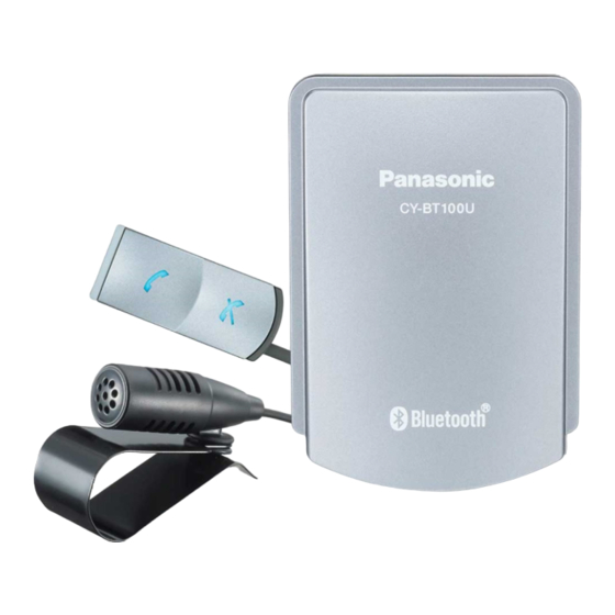
Panasonic CY-BT100U Service Manual
Hands-free kit featuring bluetooth technology
Hide thumbs
Also See for CY-BT100U:
- Operating instructions manual (92 pages) ,
- Operating instructions manual (36 pages)
Summary of Contents for Panasonic CY-BT100U
- Page 1 ORDER NO. ACED051234C7 AUTOMOTIVE AFTERMARKET CY-BT100U Hands-Free Kit featuring Bluetooth technology SPECIFICATIONS Specifications*...
- Page 2 General Power Supply DC 12V (11V - 16V), Test Voltage 14.4V Negative Ground (Supplied from a head unit or a Expansion Module) Current Consumption Less than 1.0A Communication Frequency 2402 MHz - 2480 MHz Number of channels 79 channels Channel width 1.0 Mhz Communication mode Ferquency hopped spread...
-
Page 3: About Lead Free Solder (Pbf)
1. ABOUT LEAD FREE SOLDER (PbF) Distinction of PbF PCB: PCBs (manufactured) using lead free solder will have a PbF stamp on the PCB. Caution : - Pb free solder has a higher melting point than standard solder; Typically the melting point is 50 - 70°F (30 - 40°C) higher. Please use a soldering iron with temperature control and adjust it to 700 ±... -
Page 4: Wiring Connection
4. WIRING CONNECTION 5. TERMINALS DESCRIPTION... - Page 5 IC601 : C2CBFD000155 Port Description (I/O) (V) P37/TXD10/ Serial RXD1 communications CNVss Connects by resistance GND RESET System reset input Xout/P47 Crystal oscillator clock Digital GND PWR 0 Xin/P46 Crystal oscillator clock 3.3V in digital power PWR 3.2 supply P17/INT1/ Connects by CNTR0 resistance GND...
-
Page 6: Ic Block Diagram
Port Description (I/O) (V) 26 P05/AN2 HUB CONT control input 27 P04/AN3 HUB EVENT output 28 MODE 29 P03/AN4 30 P02/AN5 KEY2 input 31 P01/AN6 KEY1 input 32 P00/AN7/ Serial TXD11 communications 6. IC BLOCK DIAGRAM 6.1. Main Block IC201 : C1BB00000860 IC301 : C1AB00002417 IC502 : C0JBAR000233... - Page 7 IC603, IC606 : C0JBAB000824 IC605 : C0JBAB000835...
-
Page 8: Packing Parts List
IC703 : C0DBAMH00013 7. PACKING PARTS LIST... - Page 9 - Item numbers listed below should not order regular spare parts. (not available)
-
Page 10: Replacement Parts List
Item Part No. Part Name & Description Q'ty Remarks Inner Carton Not available (1) Not available Operating Instructions (1) Not available Owners Information Card ASMYSW100U Switch Unit (2m) L0FBBB000005 Microphone with Bracket (5m) YEAJ011812 System-up connecting cable (3m) YFX994C128ZA Double-sided Tape YFX994C129ZA Double-sided Tape YEPFZ8466... - Page 11 Ref. No. Part No. Part Name & Description Remarks Ref. No. Part No. Part Name & Description Remarks [E-4C300] Main Block C262 F1H1C104A107 Chip, 0.1 F 16WV IC's AND TRANSISTER C301 F1H1C104A107 IC201 C1BB00000860 Chip, 0.1 F 16WV IC301 C1AB00002417 C302 F1K0J476A003 F 6.3WV...
- Page 12 Ref. No. Part No. Part Name & Description Remarks Ref. No. Part No. Part Name & Description Remarks R605 D0GB473JA008 Chip, 47k C708 F1J1C105A173 Chip, 1 F 16WV R606 D0GB102JA008 Chip, 1k 1/10W C709 F1J0J106A038 Chip, 10 F 6.3WV R607 D0GB103JA008 Chip, 10k C711 F1J1C105A173...
- Page 13 Ref. No. Part No. Part Name & Description Remarks L502 G1C100J00001 Coil L700 G1C220MA0077 Coil L701 G1C220MA0077 Coil L702 G1C100J00001 Coil L704 G1C101J00002 Coil L705 G1C221JA0036 Coil [E-4C301A] Switch Block TRANSISTERs 2SD0601AHL Transister 2SD0601AHL Transister 2SD0601AHL Transister DIODEs B3AEB0000083 LED(Blue) B3AAB0000252 LED(Red) B3AEB0000083...
-
Page 14: Exploded View
9. EXPLODED VIEW 10. WIRING DIAGRAM 10.1. Main Block (Top View) -
Page 15: Schematic Diagram
10.2. Main Block (Bottom View) 11. SCHEMATIC DIAGRAM-1 11.1. SW Block 12. SCHEMATIC DIAGRAM-2 & BLOCK DIAGRAM 12.1. Main Block 12.2. BLOCK DIAGRAM 13. SCHEMATIC DIAGRAM for Printing with Letter Size 13.1. Main Block (Left Side) 13.2. Main Block (Right Side) - Page 20 CY-BT100U...
- Page 21 12 SCHEMATIC DIAGRAM-2 & BLOCK DIAGRAM 12.1. Main Block...


Need help?
Do you have a question about the CY-BT100U and is the answer not in the manual?
Questions and answers