Nautel J1000 Repair Manual
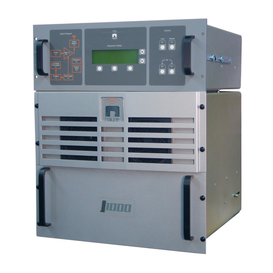
1,000 watt am broadcast transmitter
Hide thumbs
Also See for J1000:
- Repair manual (173 pages) ,
- Installation and operation manual (115 pages)
Table of Contents
Advertisement
Quick Links
J1000
1,000 Watt
AM Broadcast
Transmitter
Repair Manual
Issue 7.0 .................................. 03 June 2020
Nautel Limited
10089 Peggy's Cove Road,
Hackett's Cove, NS, Canada B3Z 3J4
T. 877 6 nautel (628835) or +1.902.823.2233
F.+1.902.823.3183
info@nautel.com
U.S. customers please contact:
Nautel Inc.
201 Target Industrial Circle, Bangor ME 04401
T. 877 6 nautel (628835) or +1.207.947.8200
F.+1.207.947.3693
info@nautel.com
e-mail: support@nautel.com
www.nautel.com
Copyright 2020 NAUTEL. All rights reserved.
Advertisement
Table of Contents
Troubleshooting

Related Manuals for Nautel J1000


Summary of Contents for Nautel J1000
- Page 1 Repair Manual Issue 7.0 ........03 June 2020 Nautel Limited 10089 Peggy's Cove Road, Hackett's Cove, NS, Canada B3Z 3J4 T. 877 6 nautel (628835) or +1.902.823.2233 F.+1.902.823.3183 info@nautel.com U.S. customers please contact: Nautel Inc. 201 Target Industrial Circle, Bangor ME 04401 T.
- Page 3 If the Buyer receives a replacement module, as part of Nautel’s module exchange program, the old module must be returned to Nautel within 30 days of receipt of the new module, at the buyers expense. If the old module is not received after 30 days, the customer will be invoiced. The buyer is responsible for installing the replacement/repaired module in the transmitter.
- Page 4 Buyer and the third party provider. 13. Nautel provides telephone and email support for its products for the life of the product at no charge. After the warranty period, parts and on-site support for the equipment are offered at a rate to be determined upon request.
- Page 5 When the warranty has expired, a charge of 80% of the list price for all exchanged modules is made. If the faulty module is returned to Nautel within 30 days, a credit is issued reducing this charge by one half to 40% of the list price.
- Page 7 NOTE A NOTE denotes important information pertaining to an operating procedure, condition, statement, etc., which is essential to highlight. A NOTE may precede or follow the text to which it applies. J1000 Repair Issue 7.0 Safety Information Page 1...
- Page 8 ‘BeO’ in the part’s description. DO NOT cut, crush or grind devices because the resulting dust may be HAZARDOUS IF INHALED. Unserviceable devices should be disposed of as harmful waste. J1000 Repair Manual Issue 7.0 Page 2...
-
Page 9: Table Of Contents
2.3.2.8.3 External 10 MHz Source 2.3.3 Interphase PDM Drive PWBs 2.3.3.1 Carrier Level Control 2.3.3.2 PDM Divider 2.3.3.3 Linear Integrator 2.3.3.4 Integrator Peak Detector 2.3.3.5 Interphase PDM Generator 2.3.3.5.1 PDM1 Generator 2.3.3.5.2 PDM2 Generator 2.3.3.6 PDM Fault Detector J1000 Repair Manual Jun.03.20... - Page 10 2.6.2.1 Carrier Reference Voltage 2-15 2.6.2.2 Alarm Threshold Circuits 2-15 2.6.2.2.1 Ac Supply Voltage 2-15 2.6.2.2.2 Reflected Power Monitor 2-15 2.6.2.2.3 RF Current Monitor 2-16 2.6.2.3 Sample Monitoring Circuits 2-17 2.6.2.3.1 B+ Voltage 2-17 2.6.2.3.2 PDM Drive 2-17 J1000 Repair Manual Jun.03.20...
- Page 11 3.4.2 Soldering Guidelines FET CHECKING/REPLACEMENT TROUBLESHOOTING REFERENCE DATA PARTS INFORMATION INTRODUCTION FAMILY TREE HOW TO LOCATE INFORMATION FOR A SPECIFIC PART 4.3.1 When Nautel Nomenclature Is Known 4.3.2 When Reference Designation Is Known REFERENCE DESIGNATION LISTS J1000 Repair Manual Jun.03.20...
- Page 12 Logic Level/Convention IDENTIFICATION OF SCHEMATIC DIAGRAMS STRUCTURE OF SCHEMATICS LOCATING THE SCHEMATIC DIAGRAM(S) FOR A FUNCTIONAL BLOCK 6-10 LOCATING A PART/ASSEMBLY IDENTIFIED ON A SCHEMATIC MECHANICAL DRAWINGS INTRODUCTION LOCATING ASSEMBLY DETAIL DRAWINGS CONTENT OF MECHANICAL DRAWINGS J1000 Repair Manual Jun.03.20...
- Page 13 List of Tables Peak Modulation Limit Threshold 2-20 Wiring Lists Provided Wiring List – J1000 Transmitter - Interconnect Wiring Wiring List – NAE88A/01D Exciter/Control Assembly Wiring List – NARA39A/01E RF Power Assembly Wiring List – NAP31/02B RF Power Module Connector Mating – J1000 Transmitter Connector Mating –...
- Page 15 Release Control Record Issue Date Reason 03 June 2020 Release 7 of product (NARA40F) J1000 Repair Manual Jun.03.20...
-
Page 17: General Information
1.1.1 Family Tree The family tree for the J1000 transmitter is depicted in Figure 4-1. It identifies the major assemblies and shows the hierarchical assembly relationship. It also identifies the reference designation assigned to each assembly and where their parts list is located. -
Page 19: Theory Of Operation
Section 2 THEORY OF OPERATION 2.1 INTRODUCTION The theory of operation for the J1000 AM broadcast transmitter is presented in this section. Unique circuits are explained. Electrical schematics, referenced throughout the text by an SD-#, are located in Section 6. -
Page 20: Exciter Interface Pwb
48-bit value to the DDS Frequency Tuning Word #1 register. The 48-bit value is written in six consecutive bytes to the DDS's six internal registers. The sclk signal is enabled on each write cycle. J1000 Repair Manual Page 2-2 Issue 7.0... -
Page 21: N Divider Control Information
It also provides control outputs that enable the RF drive tuning circuits and inhibit the pulse duration modulation (PDM) while the RF drive tuning is enabled. These inputs/ outputs are not applicable to J1000 transmitters. 2.3.2.2 Direct Digital Synthesizer The direct digital synthesizer consists of integrated circuit U5 (AD98525Q) and associated components. -
Page 22: Waveform Symmetry
2.3.2.6.1 Balanced Drive Matching Shorting shunt post E5 is installed on seven-position header XE5 to choose the optimum capacitor and resistor values. It is installed in the D position (shorting pins 7 and 8) for J1000 transmitters. 2.3.2.7 N Divider The N divider circuit is a cascade counter made up of integrated circuits U6, U7, and inverters U8:A and U8:F. -
Page 23: External 10 Mhz Source
B+ ref (1) input and, in turn, the output of buffer U3D (TP3), are a nominal 6.1 V. The resulting current flow through R20 is U6's I input. J1000 Repair Manual Page 2-5 Section 2 Theory of Operation... -
Page 24: Pdm Divider
(J1-2) is 0 V. It also ensures the RF output is reduced to near 0 W at the 100% modulation envelope valleys when operating at the transmitter's rated carrier level. J1000 Repair Manual Page 2-6 Section 2 Theory of Operation... -
Page 25: Interphase Pdm Generator
C58's charge voltage is less positive than the reference voltage. U12A's output will switch to a current-sink-to-ground when C58's charge voltage goes more positive than the reference voltage. J1000 Repair Manual Page 2-7 Section 2 Theory of Operation... -
Page 26: Shutback Latch
(J1-11) is activated (5 V). This condition is maintained until the flip-flop is reset by the removal of the logic low from U9-5 (no PDM fault) and the application of logic low to U9-1 (a logic true current-sink-to-ground reset PDM command is applied to J1-1). J1000 Repair Manual Page 2-8 Issue 7.0... -
Page 27: Pdm Inhibit
Opto-coupler U2 will turn on and apply a ground potential (0 V) to the LVPS Fail output for that PWB. J1000 Repair Manual Page 2-9 Section 2 Theory of Operation... -
Page 28: Ac/Rf Power Stage
Temperature sensor U11, operational amplifier U5:A and associated components form a temperature monitoring circuit for the RF power module. A dc voltage, representative of the temperature, is applied to Temperature output (J1-12). J1000 Repair Manual Page 2-10 Issue 7.0 Section 2 Theory of Operation... -
Page 29: Power Module Interface Pwb
PDM (B+) signal. Capacitor C5 in conjunction with L3 is resonant at a frequency to provide optimal rejection of the PDM frequency. J1000 Repair Manual Page 2-11 Section 2 Theory of Operation... -
Page 30: Power Amplifier
If the filter is designed to pass the switching frequency, but attenuate its harmonics, a sine wave is applied to the load. Figure 2-3: Simplified Principles of Class 'D' Operation J1000 Repair Manual Page 2-12 Issue 7.0 Section 2 Theory of Operation... -
Page 31: Rf Combiner/Filter Stage
50 , the RF current waveform is in-phase and of equal amplitude to the RF voltage waveform on one half of T1’s center-tapped secondary and equal amplitude, but 180 out-of- phase on the other half. J1000 Repair Manual Page 2-13 Section 2 Theory of Operation... -
Page 32: Front Panel Metering
When RF On is selected (enabled in Local mode only), the transmitter’s RF power stage is enabled to provide an RF output. When RF Off is selected (enabled in Local and Remote modes), the transmitter’s RF power stage is inhibited. J1000 Repair Manual Page 2-14 Issue 7.0... -
Page 33: Controller/Display Pwb
The refld pwr input (J7-4) is a dc voltage that is proportional to the reflected power sensed at the transmitter's output. The input is filtered and applied to the Ext Refld Pwr Sample output (J1-5) for remote monitoring. J1000 Repair Manual Page 2-15 Section 2 Theory of Operation... -
Page 34: Rf Current Monitor
Output Network lamp will continue to display a fault as a maintenance aid. The lamp will remain on until reset by the diagnostic display menu. J1000 Repair Manual Page 2-16 Issue 7.0... -
Page 35: Sample Monitoring Circuits
U32B and associated components and applied to the Ext Audio output (J1-7), then applied to the remote interface PWB for external monitoring. The Ext Mod % Sample and Audio (Speaker) outputs are not used in J1000 transmitters. 2.6.2.3.6 Low Voltage Power Supplies Attenuated, buffered samples of all low voltage dc power supplies (+24 V, ... -
Page 36: Microcontroller
50 mA. +24 V is available for use by the remote monitoring circuits on TB4-18. J1000 Repair Manual Page 2-18 Issue 7.0... -
Page 37: Audio Input
RF stress current threshold for a specific carrier level/audio amplitude/audio frequency combination (see Table 2-1). SET THRESHOLD potentiometer R45 is adjusted to precisely set the threshold voltages, when the PWB is installed in a transmitter. J1000 Repair Manual Page 2-19 Section 2 Theory of Operation... -
Page 38: Audio Chopper
PDM driver PWB is installed in its host transmitter. It has sufficient range to set the modulation depth at 100% when the audio input is between 0 dBm and +12 dBm. J1000 Repair Manual Page 2-20 Issue 7.0... -
Page 39: Audio Filter
See the NxLink manual. An optional NxLink Ethernet interface module (U200) converts the internal serial protocol to Ethernet for external interfacing. When U200 is used, internal transmitter wiring is provided to supply the module’s +15 V power supply. J1000 Repair Manual Page 2-21 Section 2 Theory of Operation... -
Page 41: Component Level Troubleshooting
Testing and maintenance equipment, including soldering and unsoldering tools, should be suitable for contact with static sensitive semiconductor devices. A 40 W, temperature controlled soldering iron is recommended. J1000 Repair Manual Page 3-1 Section 3 Component Level Troubleshooting Issue 7.0... -
Page 42: Component Replacement Precautions
SMT components are predominantly on controller/display PWB 1A1 and remote interface PWB 1A2. The RF synthesizer PWB(s) (1A4 and, if installed, 1A6) has two SMT integrated circuits. SMT components are 0603 – 6 mm x 3 mm. J1000 Repair Manual Page 3-2 Issue 7.0... -
Page 43: Fet Checking/Replacement
power MOSFET Q1 (Nautel Part # QAP49) of modulator A3 power MOSFETs Q1 through Q4 (Nautel Part # QAP75) of power amplifier A5 FETs Q1 and Q2 (Nautel Part # QR54) of forward converter PWB A1. (a) Unsolder the gate pins of the device under test and all parallel devices. Refer to the assembly’s electrical schematic in Section 6 to determine the parallel devices, if... - Page 44 (l) Reinstall the device on its associated, cleaned heat sink using the hardware removed in step (j). The Belleville (cupped) washer must be replaced with a new washer (Nautel Part # HZ48, located in ancillary kit). Both sides of the insulator (if replaced) should have a thin, even coat of thermal compound applied.
-
Page 45: Troubleshooting Reference Data
Section 6 of this manual. WARNING Nautel does not recommend troubleshooting the RF power module’s forward converter PWB (2A1A1 or 2A2A1) while the transmitter is turned on. Voltages that are hazardous to life are present near the step-up transformer (T4) on the PWB. - Page 46 (Measured at E1 of modulator 2A1A3 or 2A2A3 or at ‘B’ terminal of modulator filter PWB 2A1A4 or 2A2A4) Figure 3-3: RF Drive Input to Power Amplifier (Measured at CR5-Anode of power amplifier 2A1A5 or 2A2A5) J1000 Repair Manual Page 3-6 Issue 7.0...
-
Page 47: Power Amplifier Fet Gate Input
(Measured at gate of Q1 through Q4 of power amplifier 2A1A5 or 2A2A5) Figure 3-5: RF Output of Power Amplifier (Measured at E2 or E3 of power amplifier 2A1A5 or 2A2A5) J1000 Repair Manual Page 3-7 Section 3 Component Level Troubleshooting... - Page 48 (Measured at U1-Out of RF synthesizer PWB 1A4 or 1A6. REFERENCE (A) jumper E1 installed in INT position) Figure 3-7: 10 MHz Reference Signal for RF Synthesizer PWB (Measured at TP1 of RF synthesizer PWB 1A4 or 1A6) J1000 Repair Manual Page 3-8 Issue 7.0...
- Page 49 (Measured at TP2 of RF synthesizer PWB 1A4 or 1A6) Figure 3-9: 2PDM Output of RF Synthesizer (Measured at J1-25 or U8-12 of RF synthesizer PWB 1A4 or 1A6) J1000 Repair Manual Page 3-9 Section 3 Component Level Troubleshooting Issue 7.0...
- Page 50 Figure 3-10: 4c/B Signal (Measured at U10-4 of RF synthesizer PWB 1A4 or 1A6) Figure 3-11: 4c 4 Circuit Output (Measured at U12-1 of RF synthesizer PWB 1A4 or 1A6) J1000 Repair Manual Page 3-10 Issue 7.0 Section 3 Component Level Troubleshooting...
-
Page 51: Audio Chopper
Figure 3-12: Unbalanced Audio (Measured at U9-8 of remote interface PWB 1A2) Figure 3-13: Audio Chopper (Measured at TP7 of remote interface PWB 1A2) J1000 Repair Manual Page 3-11 Section 3 Component Level Troubleshooting Issue 7.0... - Page 52 (Measured at J1-7 or U1-3 of interphase PDM driver PWB 1A5 or 1A7) Figure 3-15: PDM – Linear Integrator Input (Measured at TP2 of interphase PDM driver PWB 1A5 or 1A7) J1000 Repair Manual Page 3-12 Issue 7.0 Section 3 Component Level Troubleshooting...
-
Page 53: Linear Integrator (Ramp) Output
(Measured at TP7 of interphase PDM driver PWB 1A5 or 1A7) Figure 3-17: Interphase PDM Generator (PDM1) Output (Measured at TP17 of interphase PDM driver PWB 1A5 or 1A7) J1000 Repair Manual Page 3-13 Section 3 Component Level Troubleshooting Issue 7.0... -
Page 55: Parts Information
To locate the information for a specific part, the assigned reference designation for the part must be known. In addition, the Nautel nomenclature (e.g., NAP31/02B) assigned to the assembly containing the part or the full reference designation, including the reference designation of all higher assemblies, must be known. -
Page 56: Reference Designation Lists
This number represents the level of a component in relation to the highest-level parts list. In this case the highest-level parts list is the J1000’s overall parts list, or the top block in the family tree shown in Figure 4-1. -
Page 57: Description Column
This section includes Nautel part numbers only. It does not include original equipment manufacturer (OEM) information (i.e., vendor part numbers). Some vendor information is provided in the J1000 documentation, otherwise contact Nautel to order a replacement part or to request assistance to find a suitable replacement. - Page 58 POWER AMPLIFIER CONTROL PANEL MOUNTING PLATE DETAIL ASSY NOT USED 197-3015-02 NAAA05/02A (SEE PART NUMBER INDEX) 197-8000-06-FAM01 VA Figure 4-1 Family Tree – J1000 1,000 Watt AM Broadcast Transmitter J1000 Repair Manual Page 4-4 Issue 7.0 Section 4 Parts Information...
- Page 59 RX47 Res,Wirewound,Silicon,225w,150 ohms,Brckt R01, R02, R03 197-8008-02 Ancillary Kit, J1000 175-5030-03 Equipment Hardware Kit (Metric ) 197-5031 J1000 Output Connector Hardwar e Kit 197-8010-06 Output Connector Assy - 7/8 EIA 197-8010-07 Output Connector Assy - STUD 197-8040 10MHz Cable JDP24...
- Page 60 NARA40F Page 2 of 19 StockCode: Description: Final Assembly, J1000, Component Lvl, StockCode Description Reference Designation JP45 Conn, Recept, Ribbon Cable, 20 pin W100P2, W100P3 JP51 Conn, Recept, Ribbon Cable, 40 pin W100P1 JT30 Conn, IDC, D-Sub, S, HDE-20, 2 5-Pos...
- Page 61 NARA40F Page 3 of 19 StockCode: Description: Final Assembly, J1000, Component Lvl, StockCode Description Reference Designation JQ16 Conn, Header, SIP, 12 Pin Breakaway, 10 Ctr J06, J10 JS43 Conn, Plug, D-Sub, 25 pin, Ver t PWB JT58 Conn, Socket, Breakaway, PWB Mt, .1 Ctr...
- Page 62 NARA40F Page 4 of 19 StockCode: Description: Final Assembly, J1000, Component Lvl, StockCode Description Reference Designation RFFS49 Resistor,SMT,MF,8250ohms,1%, 1/10W,0603 R143 RFFS50 Resistor,SMT,MF,10.0Kohms,1%, 1/10W,0603 R022, R024, R027, R028, R029, R030, R035, R043, R044, R073, R074, R075, R076, R077, R080, R083,, R084, R085,...
- Page 63 NARA40F Page 5 of 19 StockCode: Description: Final Assembly, J1000, Component Lvl, StockCode Description Reference Designation NAPE70F/01 RF Synthesizer PWB Assy 190-5043-07 IC, Programmed Microcontroller DDS CB25 Capacitor, Mica, Dipped, 100pF 2% 500V CB32 Capacitor, Mica, Dipped, 390pF 2% 500V...
- Page 64 NARA40F Page 6 of 19 StockCode: Description: Final Assembly, J1000, Component Lvl, StockCode Description Reference Designation RAB28 Resistor, MF, 1.82K Ohms, 1PC 1/4W RAB29 Resistor, MF, 2.21K Ohms, 1PC 1/4W RAB30 Resistor, MF, 2.74K Ohms, 1PC 1/4W RAB31 Resistor, MF, 3.32K Ohms, 1PC 1/4W...
- Page 65 NARA40F Page 7 of 19 StockCode: Description: Final Assembly, J1000, Component Lvl, StockCode Description Reference Designation CCFS07 Cap,SMT,Ceramic,0.1uF,10%,50V,X7R,0805 C001, C002, C003, C004, C008, C009, C010, C011, C013, C016, C017, C020, C027, C029, C037, C038,, C039, C040, C044, C045, C046, C047, C048, C061, C062, C064, C065,...
- Page 66 NARA40F Page 8 of 19 StockCode: Description: Final Assembly, J1000, Component Lvl, StockCode Description Reference Designation RAB10 Resistor, MF, 56.2 Ohms, 1PC 1 /4W R214 RAB13 Resistor, MF, 100 Ohms, 1PC 1/ 4W R200 RAB14 Resistor, MF, 121 Ohms, 1%, 1/ 4W...
- Page 67 ULCS01 IC,SMT,Comparator,Quad,SOIC-14 U11, U12 UP98 IC,SMT,Instrumentation Amp, SOIC-8 U02, U05 XFPS03 Crystal,SMT,Fund,Par Res, 3.6864MHz,Comm NAPI87A/01 Exciter Interface PWB Assy, J1000 202-5084 KC101 MOD CCG02 Capacitor, Ceramic, 0.0022uF 1 0% 100V C18, C21 CCG04 Capacitor, Ceramic, 0.01uF 10% 100V CCG07 Capacitor, Ceramic, 0.1uF 10% 100V...
- Page 68 NARA40F Page 10 of 19 StockCode: Description: Final Assembly, J1000, Component Lvl, StockCode Description Reference Designation JS12 Conn, Plug, D-Sub, 25 pin, PWB Mt J01, J02 JS13 Conn, Socket, D-Sub, 25 pin, P WB Mt J03, J04 JS18 Conn, Plug, D-Sub, 15 pin, PWB Mt...
- Page 69 NARA40F Page 11 of 19 StockCode: Description: Final Assembly, J1000, Component Lvl, StockCode Description Reference Designation CCG08 Capacitor, Ceramic, 0.22uF 10% 50V CCP36 Capacitor, Tantalum, Dipped, 1 0uF, 35V C01, C02, C03, C04, C09, C10, C12, C18, C39, C43, C47, C56,...
- Page 70 NARA40F Page 12 of 19 StockCode: Description: Final Assembly, J1000, Component Lvl, StockCode Description Reference Designation UL02 IC, Comparator, Quad UM15 IC, CMOS, Quad, 2-input NAND G Ate UM26 IC, Op Amp, Dual, Single Supply UN25 IC, Op Amp, Dual...
- Page 71 Conn, Contact, Socket, 18-14, Mate-N-Lock P01, P02 JT50 Conn, Plug, 3-Pin, Mate-N-Lok P01, P02 JT64 Conn, Pin, Header, 3-Pin Mate'n Lock J04, J05 JT80 Conn,Recept,AC,250V,20A, Quick-Dis NAP31/02B RF Power Module Assy, J1000 (Robust) A01, A02 197-1015 Ribbon Cable Assy W01, W02...
- Page 72 JT46 Conn, Contact, Socket, 18-14, Mate-N-Lock P02, P03 JT50 Conn, Plug, 3-Pin, Mate-N-Lok P02, P03 NAAA05/02A J1000 Power Amplifier Assy which uses new FET QAP7 197-1020-01 RF Drive Transformer Assy CAP16 Capacitor, Ceramic, 1.0uF 100V C01, C05, C06 CCG04 Capacitor, Ceramic, 0.01uF 10% 100V CCG07 Capacitor, Ceramic, 0.1uF 10% 100V...
- Page 73 NARA40F Page 15 of 19 StockCode: Description: Final Assembly, J1000, Component Lvl, StockCode Description Reference Designation QM45 Diode, Power Rectifier, 1000V, 8A CR01 WB37 Wire, Solderable, 155C 270/40 Litz 16AWG L01, L02, L03 NAPI73 Power Module Interface PWB Assy CCG07 Capacitor, Ceramic, 0.1uF 10% 100V...
- Page 74 NARA40F Page 16 of 19 StockCode: Description: Final Assembly, J1000, Component Lvl, StockCode Description Reference Designation QK14 Diode, LED, Amber DS01 QL23 Diode, Zener, 16V, 1.5W, 2% CR18 QM07 Diode, Zener, 5.1V, 1W, 5% CR17 QM52 Diode, Rect, 1200V,8 Amp Ultrafast, Soft Recovery...
- Page 75 NARA40F Page 17 of 19 StockCode: Description: Final Assembly, J1000, Component Lvl, StockCode Description Reference Designation TZ51 Transformer, Current Sense, Hi gh Freq TZ74 Transformer, Gate Drive, High Freq UC58 IC,Low Voltage Temp Sensor, +/-3 Deg,TO-92 UM53 Optocoupler/Optoisolator, 6-Pi n DIP...
- Page 76 NARA40F Page 18 of 19 StockCode: Description: Final Assembly, J1000, Component Lvl, StockCode Description Reference Designation RAB39 Resistor, MF, 15.0K Ohms, 1PC 1/4W R10, R11 RBP22 Resistor, Film, 33K Ohms, 5%, 2W RBP24 Resistor, Film, 68K Ohms, 5%, 2W R02, R03 RC05 Resistor, Film, 2.21 Ohms, 1%, 1/2W...
- Page 77 NARA40F Page 19 of 19 StockCode: Description: Final Assembly, J1000, Component Lvl, StockCode Description Reference Designation RBP07 Resistor, Film, 100 Ohms, 5% 2W R09, R10 RBP13 Resistor, Film, 1000 Ohms, 5%, 2W R03, R04, R05, R06, R07 RD03 Resistor, Film, 4700 Ohms, 2PC 1/2W...
-
Page 79: Wiring Information
(source/destination) inter-connecting information. Table 5-1: Wiring Lists Provided Table # Description Wiring List - J1000 Transmitter – Interconnect Wiring Wiring List - NAE88A/01D Exciter/Control Assembly Wiring List - NARA39A/01E RF Power Assembly Wiring List - NAP31/02B RF Power Module Connector Mating Information - J1000 Transmitter... -
Page 80: Wiring List - J1000 Transmitter - Interconnect Wiring
Table 5-2: Wiring List – J1000 Transmitter – Interconnect Wiring Source Destination Wire #. Color Size Remarks P104-01 P103-01 Core 1-Conductor P104-09 P103-09 Shield Shielded P104-03 P103-03 Core 1-Conductor P104-10 P103-10 Shield Shielded P104-04 P103-04 White P104-05 P103-05 Core 1-Conductor... - Page 81 White P4-05 P6-03 Black P4-06 P7-03 Black **W200P1-(+) A2TB4-18 − Blk/Grey NxLink **W200P1-(-) A2TB4-17 − NxLink NOTE: ** Wire installed only if NxLink Ethernet Interface Module (U200) is installed J1000 Repair Manual Page 5-3 Section 5 Wiring Information Issue 7.0...
-
Page 82: Wiring List - Nara39A/01E Rf Power Assembly
A4TB1-04 Yellow A4E4 L5-2 Yellow L5-1 C7-1 Yellow P03-Centre P04-Centre Core RG188A/U Coaxial Cable P03-Shell P04-Shell Shield NOTE: Wire sizes 660/46 indicate 660 strands of 46 AWG litz wire. J1000 Repair Manual Page 5-4 Issue 7.0 Section 5 Wiring Information... - Page 83 Table 5-5: Wiring List - NAP31/02B RF Power Module Source Destination Wire # Color Size Remarks P3-01 P2-01 White P3-03 P2-03 Black Table 5-6: Connector Mating Information - J1000 Transmitter Connector Mate P100 2A4J1 P101 1A1J7 P102 1A2J13 P103 1A3J8 P104 2A1A2J3...
- Page 84 A3J1 A4J2 A1P1 A2P1 Table 5-9: Connector Mating Information – NAP31/02B RF Power Module Connector Mate A1J2 A3J1 A1E1 A1E2 A1E3 W1P1 A2J2 W1P2 A3J2 W2P1 A2J1 W2P2 A5J1 J1000 Repair Manual Page 5-6 Issue 7.0 Section 5 Wiring Information...
-
Page 85: Electrical Schematics
6.6 UNIQUE SYMBOLOGY Nautel utilizes unique symbology on electrical schematics to describe two-state (logic) inputs/outputs that differ from those inputs/ outputs having only one distinct state or multiple states (analog). -
Page 86: Identification Of Schematic Diagrams
Figure 4-1 and follow the family tree branches to the block that contains the reference designation and associated Nautel nomenclature (e.g., NAP31/02B). Refer to Table 6-1 with the Nautel nomenclature number and/or the description to identify the appropriate figure number(s). -
Page 87: Electrical Schematics
The drawings in Section 7 depict the assembly detail of the transmitter and its modules/ assemblies. Refer to Table 7-1 with the name and Nautel nomenclature number of each family tree block in the path, starting at the highest assembly (normally Figure MD-1) and determine the figure number(s) for that assembly. - Page 89 DC CURRENT B AUDIO FAN FAIL B RETURN FROM RF POWER STAGE RF CURRENT SAMPLE (P100) RETURN OVER VOLT RETURN S1970125 V1 Electrical Schematic - J1000 Transmitter - Control/Monitor Function Issue 7.0 Not to Scale Figure SD-1A Sheet 1 of 2...
- Page 91 PWR 3 PWR 2 PWR 1 REMOTE RF ON AUDIO INPUT SHLD INTERLOCK INHIBIT AUTO EXCITER B EXCITER A S1970127 V2 Electrical Schematic - J1000 Transmitter - Control/Monitor Function Issue 7.0 Not to Scale Figure SD-1B Sheet 2 of 2...
- Page 93 # PDM LATCH + RETURN # RESET PDM (B) - B2P1 DIG SPARE 3 DIG SPARE 4 RETURN S1970128 V1 Dimensions = mm (inches) Electrical Schematic - J1000 Transmitter – Exciter Stage Issue 7.0 Not to Scale Figure SD-2 Sheet 1 of 1...
- Page 95 A2A4E2 RETURN RETURN RETURN B+ SAMPLE RETURN DUMP B LINE 1 GROUND LINE 2/NEUTRAL S1970129 V1 Dimensions = mm (inches) Electrical Schematic - J1000 Transmitter – RF Power Stage Issue 7.0 Not to Scale Figure SD-3 Sheet 1 of 1...
- Page 97 EXTERNAL SERIAL INTERFACE EXT TXD T1OUT TP10 TP11 TP13 TP14 T2IN ADM3202ARN MICROCONTROLLER EXT RXD R1IN DATABUS R2IN TO SHEET 2 R2OUT T2OUT 4750 R1OUT RXD0 CR17 TP52 TP53 TP54 BAT54HT1 FROM SHEET 3 R263 R264 R265 T1IN TXD0 R266 I/O7 MOSI 4750...
- Page 99 DATABUS DIGITAL INPUTS RESET CPLD ADDRESS SHEET 1 FROM U16:H SHEET 1 U16:G U16:F #LOW_BAT- U16:E U16:D U16:C #AC_LOW- U16:B #REFLD_PWR_SHUTBACK+ FROM U16:A SHEET 4 VCC_INT #HIGH_RF_CURRENT+ 0.01 11 LATCH ENABLE #REMOTE_STATUS+ U16:I 0.01 SN74AHC573DW VCC_INT #RF_ON+ R126 R125 R195 OUTPUT 10.0K 10.0K...
- Page 101 TP20 U24:C TP29 U2:H MC1413BD R108 C116 TP24 C124 C129 0.01 1500 U27:D TP30 SPARE#1_REF R101 U7:E +15V -15V +15V +15V MC33074D C117 C114 C125 C130 +15V 0.01 +24V FANS (A) R105 TP26 +24V FANS (A) U24:A +24V FANS (B) U9:G MM74HC14M TP31...
- Page 103 C172 C179 RF_CURRENT_SAMPLE TP42 U37:C TO SHEET 3 R252 U20:E U33:B R227 R236 R244 RF CURRENT 475K 475K 475K R205 C162 C186 R214 1000 0.001 U20:F U2:G R186 U20:G U32:B U32:A R243 TP58 R226 R251 100K U26:A TP51 U12:F 4750 #HIGH_RF_CURRENT+ U23:B 1500...
- Page 105 U9:E +15V -15V MC33074AD U2:B +15V -15V AD620R TRIM TRIM U11:C U4:A EXT FORWARD PWR SAMPLE +15V FWD PWR SAMPLE 33.2K 3320 10.0 0.01 47.5K 1000 U11:D THRESHOLD U11:E +15V -15V MC3302D 56.2K U4:B EXT B+ SAMPLE U4:E +15V B+ SAMPLE MC33074AD 1000 10.0...
- Page 107 U15:A RESET EXT RF ON STATUS - R106 0.01 10.0 0.01 U15:B U13:H EXT REMOTE STATUS - MC1413BD R107 10.0 1SMB5939B U15:C EXT POWER 1 STATUS - R108 10.0 U15:H +24V +24V MC74HC595AD MC1413BD U15:D 0.01 1SMB5939B EXT POWER 2 STATUS - R109 10.0 -15V...
- Page 109 RESET PD.3 R166 PD.4 10.0K C123 C125 C127 PD.5 ADM803MAKS RESET RESET 0.01 0.001 C122 PB.0 AVCC 0.01 AREF PC.2 U33:E XTAL1 PC.3 0.01 C124 MC74HC125AD PC.4 18pF 3.6864MHz R170 PC.5 E18:3 XTAL2 10.0K PDM_ANT_CURR C126 +24V OC1A TO SHEET 1 R141 18pF E18:2...
- Page 111 +15V SYNTHESIZER (A) # PDM LATCH A + +15V +15V MOD DRIVE (A) +24V # PDM LATCH B + K2:A +24V 33 +24V PA VOLTS SAMPLE (A) PA VOLTS (A) +15V MOD DRIVE (B) PA VOLTS SAMPLE (B) PA VOLTS (B) +15V SYNTHESIZER (B) +15V -15V...
- Page 113 4FC/B +3.3V-D +3.3V-D +3.3V-D # DDS INHIBIT + 4750 P1.7 2N3904 MBD301 +3.3V-D # RESET DDS + P1.6 4750 E3:3 E3:2 # HIGH BAND - 4750 +3.3V-D P3.2/INT0 P3.0/RxD HIGH 2N3904 +3.3V-D E3:1 # TUNE RF DRIVE + 4750 P1.0/T2 +5V-B 2N3904 P3.1/TxD...
- Page 115 4FC/B 2740 1210 +15V-A BALANCED DENOTES FREQUENCY DEPENDENT PART. DRIVE REFER TO REF DES INDEX FOR VALUE/PART NUMBER. 1 E5:A 1000 RF DRIVE SYMMETRY 3 E5:B SYMMETRY ADJust +15V-C +15V-A +15V-A 0.47 U10:D 5 E5:C E6:3 DISABLE RF DRIVE 3320 2N2219A 4750 ENABLE...
-
Page 117: Unbalanced Audio
2.21M +15V-B INTEGRATOR 330pF PEAK DETECTOR TP19 TP15 TP16 1500 U7:A U1:A 100pF U12:C F PDM 0.047 1000 +15V-A 2 FPDM 1000 100pF 2.21M LINEAR 1210 1000 INTEGRATOR U8:A TP10 PDM DIVIDER U5:A +15V-A 2.21M 0.22 33.2K E1:3 E2:3 U2:C U13:B DUMP U2:D... - Page 119 ALTERNATE +24V +24V +24V RETURN ALTERNATE +15V -15.8V -15V MBR1645 1000 0.47 0.01 MUR120 1000 MUR120 0.5W OUTPUT FDBK MC33167TV ALTERNATE -15V 0.47 +15.8V +15V CR17 68.1K 6810 1000 1000 0.47 0.01 0.47 1N4746A 1000 MUR1520 1000 RXE250 0.5W MUR1520 +24.8V 2210 +24.8V...
- Page 121 FAN TACH FAN ENABLE +24V FAN 1 DC CURRENT FAN FAIL +24V RETURN +24V FORWARD CONVERTER RETURN 0.12 450V 450V 450V # INHIBIT + W1P2 W1P1 B+ SAMPLE OUTPUT ADJUST 1 B+ ON OUTPUT ADJUST 2 LINE AC INPUT LINE 1N4743A MODULATOR 1820...
- Page 123 +18V +18V OUTPUT ADJUST 2 +18V +18V MOC8104 OUTPUT ADJUST 1 MOC8104 U5:E +18V MC34074 DC OUTPUT 0.01 0.001 300μH 600V CR13 0.01 HFA08TB120 220pF HFA08TB120 1.0M 0.5W SIOV-S14K300 HFA08TB120 DSP25-16A AC INPUT 0.015 3.32M 580uH 22.1K 22.1K 300μH SIOV-S14K300 100K 100K 450V...
-
Page 125: Mechanical Drawings
Table 7-1: Mechanical Drawings Figure # Description MD-1 Assembly Detail/Dimensional Information - J1000 AM Broadcast Transmitter MD-2 Assembly Detail – NAE88A/01D Exciter/Control Assembly MD-3 Assembly Detail – NAPC143B/01 Controller/Display PWB MD-4 Assembly Detail –... - Page 127 Dimensions = mm (inches) Assembly Detail/Dimensional Information - J1000 AM Broadcast Transmitter Issue 7.0 Not to Scale Figure MD-1 Sheet 1 of 1...
- Page 129 TOP VIEW Remote Interface Interphase PDM RF Synthesizer Driver PWBs PWBs Exciter Interface Controller/Display Ethernet Interface Module Power Supply (Optional) Assembly U200 LVPS Buck Converter PWB Dimensions = mm (inches) Assembly Detail - NAE88A/01C Exciter/Control Assembly Issue 7.0 Not to Scale Figure MD-2 Sheet 1 of 1...
- Page 131 R181 R174 R171 C131 C139 C118 R175 R200 R199 R105 R138 R164 R204 R203 R136 C160 C159 R133 NAUTEL ASSY 197-2050 C195 TRANSMITTER CONTROLLER/DISPLAY R137 NAPC SER. R193 R264 CR17 CR15 R140 R195 R110 R125 R251 C111 R142 C104 TP58...
- Page 133 R100 SINGLE SINGLE C86 C87 DIFF DIFF C105 R108 R106 R107 R109 R110 R111 R112 R113 R114 R115 R154 NAUTEL ASSY 197-2065 REMOTE INTERFACE C93 C94 R155 C116 CR26 NAPI SER. CR38 CR27 C115 C122 CR25 CR24 R166 C114 C123...
- Page 135 IPM GAIN 1 IPM GAIN 2 GRID2 A B C D E F GRID1 NAUTEL ASSY 197-4050 EXCITER INTERFACE NAPI SER. A B C D E F M1970120 V1 Assembly Detail – NAPI87A/01 Exciter Interface PWB Issue 7.0 Not to Scale...
- Page 137 IPM BAL RF SYNTHESIZER M3 HEX NUT 10MHz NAPE70 SER. #4 BELLEVILLE WASHER INPUT M3 WASHER SEMICONDUCTOR HEATSINK (OMIT FOR U11) SYMMETRY ADJ EXT INT M3 PAN HEAD SCREW ENABLE DISABLE U9 & U11 MOUNTING DETAIL TORQUE ATACHING HARDWARE TO 4.0 INCH POUNDS (0.45 NEWTON METERS) HIGH SOURCE...
- Page 139 DUMP TP16 TP15 GAIN TP18 INTERPHASE PDM DRIVER NAPM10 SER. M1970092 V2 Dimensions = mm (inches) Assembly Detail – NAPM10B Interphase PDM Driver PWB Issue 7.0 Not to Scale Figure MD-7 Sheet 1 of 1...
- Page 141 NAUTEL ASSY 195-7025 LVPS BUCK CONVERTER NAPS SER. M3 PAN HEAD SCREW SEMICONDUCTOR HEATSINK CR11 M3 WASHER # 4 BELLEVILLE WASHER M3 HEX NUT Q1 & Q2 MOUNTING DETAIL TORQUE ATTACHING HARDWARE TO 4.0 INCH POUNDS (0.45 NEWTON METRES) CR10...
- Page 143 RF Power Modules ‘B’ ‘A’ Forward/Reflected Power Probe J5 J4 RF Filter Input PWB REAR VIEW BOTTOM VIEW Spark Dimensions = mm (inches) Assembly Detail – NARA39A/01E RF Power Assembly Issue 7.0 Not to Scale Figure MD-9 Sheet 1 of 1...
- Page 145 Dimensions = mm (inches) Assembly Detail – NAP31/02B RF Power Module Issue 7.0 Not to Scale Figure MD-10 Sheet 1 of 1...
- Page 147 NAUTEL ASSY 197-7022 FORWARD CONVERTER NAPS SER. M3 PAN HEAD SCREW # 4 BELLEVILLE WASHER M3 WASHER SEMICONDUCTOR CR11 HAT46 HEATSINK Q1 & Q2 MOUNTING DETAIL CR15 TORQUE ATTACHING HARDWARE TO 6.0 INCH POUNDS (0.68 NEWTON METRES) AC IND CR10...
- Page 149 NAUTEL ASSY 197-1095 POWER MODULE INTERFACE NAPI SER. DUMP Fpdm RF DRIVE M1970015 V1 Dimensions = mm (inches) Assembly Detail – NAPI73 Power Module Interface PWB Issue 7.0 Not to Scale Figure MD-12 Sheet 1 of 1...
- Page 151 M3 PAN HEAD SCREW M3 WASHER SHOULDER WASHER SEMICONDUCTOR INSULATOR CHASSIS M3 WASHER # 4 BELLEVILLE WASHER MODULATOR M3 HEX NUT NASM SER. CAUTION HIGH VOLTAGE PRESENT TORQUE ATTACHING HARDWARE TO WHEN LAMP IS ON 4.0 INCH POUNDS (0.45 NEWTON METRES) CR11 CR10 M3 PAN HEAD SCREW...
- Page 153 M1970054 V1 Dimensions = mm (inches) Assembly Detail – NAPF08 Modulator Filter PWB Issue 7.0 Not to Scale Figure MD-14 Sheet 1 of 1...
- Page 155 M3 PAN HEAD SCREW #4 BELLEVILLE WASHER M3 WASHER TRANSISTOR INSULATOR THERMAL CHASSIS COMPOUND HEATSINK TORQUE ATTACHING HARDWARE TO 4.0 INCH POUNDS (0.45 NEWTON METRES) TRANSFORMER T1 CONNECTIONS. TWIST GROUPED WIRES TOGETHER ORANGE + PAD NEAR R2 YELLOW + PAD NEAR R2 ORANGE/BLACK - PAD NEAR R2 YELLOW/BLACK...
- Page 157 BAND L1-2 L1-3 HIGH NAUTEL ASSY 197-6030 RF FILTER INPUT NAPF SER. M1970064 V1 Dimensions = mm (inches) Assembly Detail – NAPF03A/01 RF Filter Input PWB Issue 7.0 Not to Scale Figure MD-16 Sheet 1 of 1...
- Page 159 BAND L4-2 L4-3 HIGH M1950347 V1 Dimensions = mm (inches) Assembly Detail – NAPF07C/03 Forward/Reflected Power Probe Issue 7.0 Not to Scale Figure MD-17 Sheet 1 of 1...
Need help?
Do you have a question about the J1000 and is the answer not in the manual?
Questions and answers