Table of Contents
Advertisement
Advertisement
Table of Contents

Related Manuals for Clevo PB70ED


Summary of Contents for Clevo PB70ED
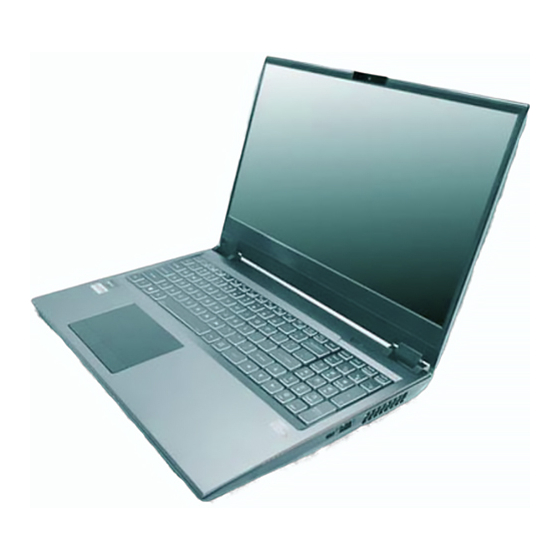
- Page 1 PB70ED / PB71ED...
- Page 3 Preface Notebook Computer PB70ED / PB71ED Service Manual...
- Page 4 Preface Notice The company reserves the right to revise this publication or to change its contents without notice. Information contained herein is for reference only and does not constitute a commitment on the part of the manufacturer or any subsequent ven- dor.
- Page 5 This manual is intended for service personnel who have completed sufficient training to undertake the maintenance and inspection of personal computers. It is organized to allow you to look up basic information for servicing and/or upgrading components of the PB70ED / PB71ED series notebook PC.
- Page 6 Preface IMPORTANT SAFETY INSTRUCTIONS Follow basic safety precautions, including those listed below, to reduce the risk of fire, electric shock and injury to per- sons when using any electrical equipment: 1. Do not use this product near water, for example near a bath tub, wash bowl, kitchen sink or laundry tub, in a wet basement or near a swimming pool.
- Page 7 Preface Instructions for Care and Operation The notebook computer is quite rugged, but it can be damaged. To prevent this, follow these suggestions: Don’t drop it, or expose it to shock. If the computer falls, the case and the components could be damaged. Do not expose the computer Do not place it on an unstable Do not place anything heavy...
- Page 8 Preface Avoid interference. Keep the computer away from high capacity transformers, electric motors, and other strong mag- netic fields. These can hinder proper performance and damage your data. Take care when using peripheral devices. Use only approved brands of Unplug the power cord before peripherals.
- Page 9 Preface Battery Precautions • Only use batteries designed for this computer. The wrong battery type may explode, leak or damage the computer. • Do not continue to use a battery that has been dropped, or that appears damaged (e.g. bent or twisted) in any way. Even if the computer continues to work with a damaged battery in place, it may cause circuit damage, which may possibly result in fire.
- Page 10 Preface Related Documents You may also need to consult the following manual for additional information: User’s Manual on CD/DVD This describes the notebook PC’s features and the procedures for operating the computer and its ROM-based setup pro- gram. It also describes the installation and operation of the utility programs provided with the notebook PC. System Startup 130°...
-
Page 11: Table Of Contents
Preface Contents Introduction ..........1-1 Main Board ................... A-5 HDD ....................A-6 Overview ..................1-1 LCD ....................A-7 Specifications ..................1-2 Schematic Diagrams......... B-1 External Locator - Top View with LCD Panel Open ......1-4 External Locator - Front & Right Side Views .........1-5 System Block Diagram ..............B-2 External Locator - Left Side &... - Page 12 Preface GPU 5/6 ..................B-28 TR-TBT ..................B-60 IFP I/O Interface ................B-29 AR_TBT_SP PWR ...............B-61 GPU 6/6 ..................B-30 TPS65987 ..................B-62 GPU NVVDD, FBVDDQ ............B-31 TBT/Type C ..................B-63 GPU GND ..................B-32 Conn_to Extend Board ..............B-64 GPU Decoupling ................B-33 3.3VA, 3.3V, 3.3VS, 5VS ............B-65 GPU Decoupling 2 ...............
- Page 13 Preface Speaker Con ................. B-92...
- Page 14 Preface...
-
Page 15: Introduction
Chapter 1: Introduction Overview This manual covers the information you need to service or upgrade the PB70ED / PB71ED series notebook computer. Information about operating the computer (e.g. getting started, and the Setup utility) is in the User’s Manual. Information about dri-vers (e.g. -
Page 16: Specifications
Introduction Specifications Processor Options Video Adapter Options i7-8750H (2.20GHz) Microsoft Hybrid Graphics Mode or Discrete Graphics Mode 9MB Smart Cache, 14nm, DDR4-2666MHz, TDP 45W Supports up to 4 Active Displays i5-8300H (2.30GHz) Supports NVIDIA Surround View via HDMI x 1, MiniDP x1 9MB Smart Cache, 14nm, DDR4-2666MHz, TDP 45W Latest Specification Information and Display Port over Type-C... - Page 17 Introduction Audio Interface Environmental Spec High Definition Audio Compliant Interface One USB 3.1 Gen 2 Type-C Port* Temperature ° ° S/PDIF Digital Output *The maximum amount of current supplied by USB Type-C Operating: 5 C - 35 ports is 500mA (USB 2.0)/900mA (USB 3.1). Built-In Array Microphone Non-Operating: -20°C - 60°C Two Speakers...
-
Page 18: External Locator - Top View With Lcd Panel Open
Introduction External Locator - Top View with LCD Panel Open Figure 1 Top View 1. PC Camera 2. *PC Camera LED *When the PC camera is in use, the LED will be illuminated. 3. Built-In Array Microphone 4. LCD 5. Power Button 6. -
Page 19: External Locator - Front & Right Side Views
Introduction External Locator - Front & Right Side Views Figure 2 Front View 1. LED Indicator 2. Multi-in-1 Card Reader FRONT VIEW Figure 3 Right Side View 1. USB 3.1 Gen 2 Type-C Port (Factory Option) RIGHT SIDE VIEW Thunderbolt 3 Port 2. -
Page 20: External Locator - Left Side & Rear View
Introduction External Locator - Left Side & Rear View Figure 4 Left Side View 1. Security Lock Slot 2. Vent 3. *Powered USB LEFT SIDE VIEW 3.0 (USB 3.1 Gen 1) Type-A Port 4. 2-In-1 Audio Jack (Microphone and S/PDIF Optical) 5. -
Page 21: External Locator - Bottom View
Introduction External Locator - Bottom View Figure 6 Bottom View 1. Vent 2. Battery 3. Speakers 4. Subwoofer Overheating To prevent your com- puter from overhea- ting, make sure no- thing blocks any vent while the computer is in use. External Locator - Bottom View 1 - 7... -
Page 22: Mainboard Overview - Top (Key Parts)
Introduction Mainboard Overview - Top (Key Parts) Figure 7 Mainboard Top Key Parts 1. KBC-ITE IT8587 1 - 8 Mainboard Overview - Top (Key Parts) -
Page 23: Mainboard Overview - Bottom (Key Parts)
Introduction Mainboard Overview - Bottom (Key Parts) Figure 8 Mainboard Bottom Key Parts 1. PCH 2. GPU 3. CPU 4. Memory Slots DDR4 SO-DIMM 5. Mini-Card Connector (M.2 PCIE/SATA SSD Module) 6. Mini-Card Connector (M.2 PCIE Module) 7. Mini-Card Connector (WLAN Module) Mainboard Overview - Bottom (Key Parts) 1 - 9... -
Page 24: Mainboard Overview - Top (Connectors)
Introduction Mainboard Overview - Top (Connectors) Figure 9 Mainboard Top Connectors 1. Per Key Cable Connector 2. Keyboard Cable Connector 3. RGB Keyboard Cable Connector 4. Power Switch Connector 5. Multi-in-1 Card Reader 6. USB 3.1 Gen 2 Type-C Port (Factory Option) Thunderbolt 3 Port... -
Page 25: Mainboard Overview - Bottom (Connectors)
Introduction Mainboard Overview - Bottom (Connectors) Figure 10 Mainboard Bottom Connectors 1. RJ-45 LAN Jack 2. HDMI-Out Port 3. Mini DisplayPort 4. DisplayPort 1.3 over USB 3.1 Gen 2 Type-C Port 5. USB 3.0 (USB 3.1 Gen 1) Type-A Port 6. - Page 26 Introduction 1 - 12...
-
Page 27: Disassembly
Chapter 2: Disassembly Overview This chapter provides step-by-step instructions for disassembling the PB70ED / PB71ED series notebook’s parts and subsystems. When it comes to reassembly, reverse the procedures (unless otherwise indicated). We suggest you completely review any procedure before you take the computer apart. -
Page 28: Maintenance Tools
Disassembly NOTE: All disassembly procedures assume that the system is turned OFF, and disconnected from any power supply (the battery is removed too). Maintenance Tools The following tools are recommended when working on the notebook PC: • M3 Philips-head screwdriver •... -
Page 29: Maintenance Precautions
Disassembly Maintenance Precautions The following precautions are a reminder. To avoid personal injury or damage to the computer while performing a re- moval and/or replacement job, take the following precautions: Power Safety Don't drop it. Perform your repairs and/or upgrades on a stable surface. If the computer falls, the case and other components Warning could be damaged. -
Page 30: Disassembly Steps
Disassembly Disassembly Steps The following table lists the disassembly steps, and on which page to find the related information. PLEASE PERFORM THE DISASSEMBLY STEPS IN THE ORDER INDICATED. To remove the Keyboard: To remove the Wireless LAN Module: 1. Remove the battery page 2 - 5 1. -
Page 31: Removing The Battery
Disassembly Removing the Battery Figure 1 Battery Removal 1. Turn off the computer, turn it over. 2. Remove screws (Figure 1a). a. Remove the screws. 3. Carefully lift the battery up in the direction of the arrow at point (Figure 1b b. -
Page 32: Removing The Keyboard
Disassembly Removing the Keyboard Figure 2 Keyboard Removal 1. Turn off the computer, turn it over. 2. Remove screws from the bottom of the computer. a. Remove the screws from 3. Open it up with the LCD on a flat surface before pressing at point to release the keyboard module (use the spe- the bottom of the compu- cial eject stick... -
Page 33: Removing The Hard Disk Drive
Disassembly Removing the Hard Disk Drive Figure 3 HDD Assembly The hard disk drive can be taken out to accommodate other 2.5" serial (SATA) hard disk drives with a height of 7mm Removal (h). Follow your operating system’s installation instructions, and install all necessary drivers and utilities (as outlined in Chapter 4 of the User’s Manual) when setting up a new hard disk. - Page 34 Disassembly 5. The HDD will be visible at point on the mainboard (Figure 4d Figure 4 6. Remove screws from the HDD assembly and disconnect the ribbon cable from the locking collar HDD Assembly socket by using a flat-head screwdriver to pry the locking collar pins away from the base (Figure 4e).
-
Page 35: Removing The System Memory (Ram)
Disassembly Removing the System Memory (RAM) Figure 5 RAM Module The computer has four memory sockets for 260 pin Small Outline Dual In-line Memory Modules (SO-DIMM) support- Removal ing DDR4 Up to 2400 MHz. The main memory can be expanded up to 64GB. The total memory size is automatically detected by the POST routine once you turn on your computer. -
Page 36: Removing The M.2 Ssd Module
Disassembly Removing the M.2 SSD Module Figure 6 M.2 SSD-1 Module M.2 SSD-1 Removal Procedure Removal 1. Turn off the computer, remove the battery (page 2 - 5), keyboard (page 2 - 6) and bottom case (page 2 - 2. The M.2 SSD module will be visible at point on the mainboard (Figure 6a). -
Page 37: Removing The Wireless Lan Module
Disassembly Removing the Wireless LAN Module Figure 7 Wireless LAN 1. Turn off the computer, remove the battery (page 2 - 5), keyboard (page 2 - 6) and bottom case (page 2 - Module Removal 2. The Wireless LAN module will be visible at point on the mainboard (Figure 7a). -
Page 38: Wireless Lan, Combo Module Cables
Disassembly Wireless LAN, Combo Module Cables Note that the cables for connecting to the antennae on WLAN, WLAN & Bluetooth Combo modules are not labelled. The cables/covers (each cable will have either a black or transparent cable cover) are color coded for identification as outlined in the table below. -
Page 39: Removing The Ccd
Disassembly Removing the CCD Figure 8 CCD Removal 1. Turn off the computer, turn it over to remove the battery (page 2 - 2. Lay the computer down on a flat surface with the top case up forming a 130 degree angle. a. - Page 40 Disassembly 5. Disconnect the cable from the locking collar socket by using a flat-head screwdriver to pry the locking collar Figure 9 pins away from the base (Figure 9c). CCD Removal 6. Remove the CCD module (Figure 9d). (cont’d) 7. Reverse the process to install a new CCD module. c.
-
Page 41: Part Lists
Appendix A:Part Lists This appendix breaks down the PB70ED / PB71ED series notebook’s construction into a series of illustrations. The com- ponent part numbers are indicated in the tables opposite the drawings. Note: This section indicates the manufacturer’s part numbers. Your organization may use a different system, so be sure to cross-check any relevant documentation. -
Page 42: Part List Illustration Location
Part List Illustration Location The following table indicates where to find the appropriate part list illustration. Table A - 1 Part List Illustration Part Location page A - 3 Bottom page A - 4 page A - 5 Main Board page A - 6 page A - 7 A - 2... -
Page 43: Top
Figure A - 1 Top A - 3... -
Page 44: Bottom
Bottom Figure A - 2 Bottom A - 4 Bottom... -
Page 45: Main Board
Main Board Figure A - 3 Main Board Main Board A - 5... -
Page 46: Hdd
Figure A - 4 A - 6 HDD... -
Page 47: Lcd
Figure A - 5 LCD A - 7... - Page 48 A - 8...
-
Page 49: Schematic Diagrams
Schematic Diagrams Appendix B: Schematic Diagrams This appendix has circuit diagrams of the PB70ED / PB71ED notebook’s PCB’s. The following table indicates where to find the appropriate schematic diagram. Diagram - Page Diagram - Page Diagram - Page Diagram - Page... -
Page 50: System Block Diagram
Schematic Diagrams System Block Diagram 9$ 9 9 96 96 3:5 6: 6+((7 () &RIIHH /DNH 6\VWHP %ORFN 'LDJUDP 6< ( $$& 9&&6)5B2& 9&&67 9&&6)5 9&&67* 19 9 6+((7 &211 9'' 9'' 7<3( & '3 5(3($7(5 3(* [ 6+((7 6+((7 &RIIHH /DNH + 9 9''4 96 977... -
Page 51: Processor 1/6
Schematic Diagrams Processor 1/6 Zo=50ohm, L<4.6" Zo=50ohm, L<4.6" M_B_DQ[63:0] M_A_DQ[63:0] U38A DIFF=88ohm, L<4.6" U38B DIFF=88ohm, L<4.6" M_A_DQ0 M_B_DQ0 BT11 M_A_CLK_DDR0 M_B_CLK_DDR0 DDR0_DQ_0/DDR0_DQ_0 DDR0_CKP_0/DDR0_CKP_0 DDR1_DQ_0/DDR0_DQ_16 DDR1_CKP_0/DDR1_CKP_0 M_A_DQ1 M_B_DQ1 BR11 DDR0_DQ_1/DDR0_DQ_1 DDR0_CKN_0/DDR0_CKN_0 M_A_CLK_DDR#0 DDR1_DQ_1/DDR0_DQ_17 DDR1_CKN_0/DDR1_CKN_0 M_B_CLK_DDR#0 M_A_DQ2 M_B_DQ2 DDR0_DQ_2/DDR0_DQ_2 DDR0_CKP_1/DDR0_CKP_1 M_A_CLK_DDR1 DDR1_DQ_2/DDR0_DQ_18 DDR1_CKP_1/DDR1_CKP_1 M_B_CLK_DDR1 M_A_DQ3... -
Page 52: Processor 2/6
Schematic Diagrams Processor 2/6 To NV From NV DIFF=85ohm, L=3"~8" DIFF=85ohm, L=3"~8" U38C PEG_TX_0 C1289 0.22u_10V_X5R_04 PEG_RX15 PEG_RXP_0 PEG_TXP_0 PEG_TX15 15 D02 0928 PEG reverse PEG_TX#_0 D02 0928 PEG reverse C1291 0.22u_10V_X5R_04 PEG_RX#15 PEG_TX#15 15 PEG_RXN_0 PEG_TXN_0 PEG_TX_1 C1290 0.22u_10V_X5R_04 PEG_RX14 PEG_RXP_1 PEG_TXP_1... -
Page 53: Processor 3/6
Schematic Diagrams Processor 3/6 DESCRIPTION U38E NORM Stall DIFF=85ohm, L=4"~9" NORM Pchless Pchless Mode BN25 CFG0 PCH_CPU_BCLK_R_DP BCLKP CFG_0 D02 0928 for PEG reverse BN27 NORM Reverse PEG_LANE_REVERSAL-SEE PCIE CHAPTER PCH_CPU_BCLK_R_DN BCLKN CFG_1 BN26 CFG2 R106 1K_04 CFG_2 BN28 Enabled Disabled Physical_Debug_Enabled PCH_CPU_PCIBCLK_R_DP... -
Page 54: Processor 4/6
Schematic Diagrams Processor 4/6 U38F U38G U38H BJ15 VSS_1 VSS_82 VSS_163 VSS_244 VSS_325 VSS_409 AL10 AY12 BJ18 VSS_2 VSS_83 VSS_164 VSS_245 VSS_326 VSS_410 AL12 AY33 BJ22 BP12 VSS_3 VSS_84 VSS_165 VSS_246 VSS_327 VSS_411 AL14 AY34 BJ25 BP14 VSS_4 VSS_85 VSS_166 VSS_247 VSS_328 VSS_412... -
Page 55: Processor 5/6
Schematic Diagrams Processor 5/6 20180509 VCORE VCORE follow PA70 VCORE VCORE U38I U38J AA13 AH13 VCC1 VCC64 22u_6.3V_X6S_08 2 *3 AA31 AH14 VCC2 VCC65 VCC1 VCC64 AA32 AH29 VCORE VCC3 VCC66 VCC2 VCC65 10u_4V_X6S_06 9 *1 AA33 AH30 VCC4 VCC67 VCC3 VCC66 AA34... - Page 56 Schematic Diagrams Processor 6/6 VCCGT VCCGT VCCSA VDDQ U38K U38L U38M 11.1A AT14 BD35 VCCGT1 VCCGT80 AT31 BD36 CPU Domain CPU Voltage CPU ICCMAX VR output Board Edge cap Backside cap VCCGT2 VCCGT81 VCCSA1 VDDQ1 AT32 BE31 AE12 SRVD_TP5 VCCGT3 VCCGT82 VCCSA2 VDDQ2...
-
Page 57: Ddr4 Cha So-Dimm_0
Schematic Diagrams DDR4 CHA SO-DIMM_0 Channel A SO-DIMM_0 STD TYPE H=8mm VDDQ VTT_MEM J_DIMMA_1A J_DIMMA_1B M_A_DQ[63:0] M_A_DQ5 M_A_CLK_DDR0 CK0_T VDD19 VDDQ M_A_DQ0 2.5V PLACE NEAR TO DIMM M_A_CLK_DDR#0 CK0_C VDD18 M_A_DQ2 M_A_CLK_DDR1 CK1_T VDD17 M_A_DQ3 M_A_CLK_DDR#1 CK1_C VDD16 VPP2 M_A_DQ1 VDD15 VPP1 R219... -
Page 58: Ddr4 Chb So-Dimm_0
Schematic Diagrams DDR4 CHB SO-DIMM_0 STD TYPE Channel B SO-DIMM_0 H=4mm J_DIMMB_2A J_DIMMB_2B VTT_MEM VDDQ M_B_DQ[63:0] M_B_DQ0 M_B_CLK_DDR0 CK0_T VDD19 VDDQ M_B_DQ5 2.5V PLACE NEAR TO DIMM M_B_CLK_DDR#0 CK0_C VDD18 M_B_DQ7 M_B_CLK_DDR1 CK1_T VDD17 M_B_DQ3 M_B_CLK_DDR#1 CK1_C VDD16 VPP2 M_B_DQ4 VDD15 VPP1 M_B_DQ2... -
Page 59: Panel
Schematic Diagrams Panel PANEL CONNECTOR PLVDD >3A 20180427 Follow common design PANEL VLED POWER C1273 C206 If no NVSR_DET# pin for NVSR panel, has the BIOS *22u_6.3V_X5R_06 1u_6.3V_X5R_02 must update to re-check new EDID issue! D02 1003A J_LCD1 doesn't exist in common design FRAME_LOCK#_R GPIO5_FRAME_LOCK# unstuff... -
Page 60: Hdmi
Schematic Diagrams HDMI HDMI CONNECTOR HDMI_5VS 20180503 HDMI_5VS Follow common design Add co-lay solution 100mA VOUT RB751S-40H 20180718 22u_6.3V_X5R_06 *22u_6.3V_X5R_06 20180420 follow PA70 cost down Del uP7549UMA5-20 *10u_6.3V_X5R_06 J_HDMI1 APL3517A PCB Footprint = m-sot23-123 R444 R443 2K_04 2K_04 HDMI_HPD-C HDMI_SCL-C HOT PLUG DETECT HDMI_5VS TMDS_DATA0... -
Page 61: Mini Dp Port
Schematic Diagrams Mini DP Port CLOSE TO CONNECTOR 3.3VS MDP_E_PW R mini-Display Port E (BACK) 20180810 VOUT Del co-lay resistors D_MDP_E3 D_MDP_E3_L D_MDP_E#3 D_MDP_E#3_L *10u_6.3V_X5R_06 10u_6.3V_X5R_06 20180718 From *DVI2012F2SF-900T05_08-SHORT Follow comm design NV Port_E To Connector 44,64 SUSB uP7549UMA5-20 DIFF=90ohm, L<6" DIFF=90ohm D_MDP_E#2 D_MDP_E#2_L... -
Page 62: Ps8330B
Schematic Diagrams PS8330B mDP REDRIVER 3.3VS 3.3VS 20180420 Del co-lay circuit From NV Port_A C1032 C1106 20180420 Del co-lay circuit MLCC Comm part DIFF=90ohm, Total L<6" R275 To TBT PS8330B_AUXn 0.1u_6.3V_X5R_02 0.01u_16V_X7R_04 C1035 0.1u_10V_X7R_04 100K_04 MDP_A_AUX#_SDA PS8330B_AUXp DIFF=100ohm, L<2" C1034 0.1u_10V_X7R_04 MDP_A_AUX_SCL 20180430 Del PS8338B... -
Page 63: Ps8331
Schematic Diagrams PS8331 CAP NEAR PS8331B 5*9mm Frome Intel PS8331B DIFF=85ohm, L=2"~4" C216 0.1u_10V_X7R_04 IEDP_TXP_0_R 3.3VS IEDP_TX_0 IN1_D0P VDD3 C210 0.1u_10V_X7R_04 IEDP_TXN_0_R PS8331_IN1_AEQ# IEDP_TX#_0 IN1_D0N IN1_AEQ# PS8331_IN2_AEQ# SB_IEDP_HPD IN1_HPD IN2_AEQ# IEDP_TXP_1_R C230 0.1u_10V_X7R_04 From PCH GPIO GPP_F9 IEDP_TX_1 IN1_D1P C231 0.1u_10V_X7R_04 IEDP_TXN_1_R PS8331_PI0... - Page 64 Schematic Diagrams GPU 1/6 NV PCI EXPRESS 20180727 Follow VGA card add 3.3V NV3V3 Place between 1/22 PCI_EXPRESS Place Under GPU GPU and PS PEX_VDD BK44 PEX_WAKE BB35 PEX_DVDD R536 R538 GPU_PEX_RST# BK26 BB36 PEX_RST PEX_DVDD 29,34 GPU_PEX_RST# *10K_04 *10K_04 BC35 C381 C382...
-
Page 65: Gpu 2/6
Schematic Diagrams GPU 2/6 GDDR6 Mode 1 Mapping GPU FRAME BUFFER PARTITION A/B GB4B-256 ch0 Bytes0,1 ch0 Bytes2,3 2/22 FBA 3/22 FBB CMD0 CA0_A FBA_D0 FBA_CMD0 FBB_D0 FBB_CMD0 CMD1 CA9_A CA9_B FBA_D0 FBA_CMD0 FBB_D0 FBB_CMD0 FBA_D1 FBA_CMD1 FBB_D1 FBB_CMD1 FBA_D1 FBA_CMD1 FBB_D1 FBB_CMD1... -
Page 66: Frame Buffer Partition A
Schematic Diagrams Frame Buffer Partition A FRAME BUFFER PARTITION A 31..0 FBA_W CK01 FBA_DBI[3..0] FBVDDQ FBA_W CK01 FBA_W CK01* FBA_DBI[3..0] FBA_W CK01* FBA_W CK23 FBA_EDC[3..0] FBA_W CK23 VRAM=K4Z80325BC-HC14 FBA_W CK23* FBA_EDC[3..0] FBA_W CK23* FBA_CMD[15..0] FBA_W CKB01 FBA_CMD[15..0] FBA_W CKB01 FBA_W CKB01* FBA_CMD32 FBA_W CKB01* FBA_CMD32... - Page 67 Schematic Diagrams Frame Buffer Partition A FRAME BUFFER PARTITION A 63..32 FBA_W CK45 FBA_DBI[7..4] FBVDDQ FBA_W CK45 FBA_W CK45* FBA_DBI[7..4] FBA_W CK45* FBA_W CK67 FBA_EDC[7..4] VRAM=K4Z80325BC-HC14 FBA_W CK67 FBA_W CK67* FBA_EDC[7..4] FBA_W CK67* FBA_CMD[31..16] FBA_W CKB45 FBA_CMD[31..16] FBA_W CKB45 FBA_W CKB45* FBA_CMD33 NORMAL FBA_W CKB45*...
-
Page 68: Frame Buffer Partition B
Schematic Diagrams Frame Buffer Partition B FRAME BUFFER PARTITION B 31..0 FBB_W CK01 FBB_DBI[3..0] FBVDDQ FBB_W CK01 FBB_W CK01* FBB_DBI[3..0] FBB_W CK01* FBB_W CK23 FBB_EDC[3..0] VRAM=K4Z80325BC-HC14 FBB_W CK23 FBB_W CK23* FBB_EDC[3..0] FBB_W CK23* FBB_CMD[15..0] FBB_W CKB01 FBB_CMD[15..0] FBB_W CKB01 FBB_W CKB01* FBB_CMD32 FBB_W CKB01* FBB_CMD32... - Page 69 Schematic Diagrams Frame Buffer Partition B FRAME BUFFER PARTITION B 63..32 FBB_W CK45 FBB_DBI[7..4] FBVDDQ FBB_W CK45 FBB_W CK45* FBB_DBI[7..4] FBB_W CK45* FBB_W CK67 FBB_W CK67 FBB_EDC[7..4] VRAM=K4Z80325BC-HC14 FBB_W CK67* FBB_EDC[7..4] FBB_W CK67* FBB_CMD[31..16] FBB_W CKB45 FBB_CMD[31..16] FBB_W CKB45 FBB_W CKB45* FBB_CMD33 NORMAL FBB_W CKB45*...
- Page 70 Schematic Diagrams GPU 3/6 GPU FRAME BUFFER PARTITION C/D GDDR6 CMD Mapping x16 Mode Lower 0..31 Upper 32..63 DRAM1 DRAM2 CHA-Byte 0,1 CHA-Byte 4,5 4/22 FBC 5/22 FBD CA0_A CMD0 CMD20 FBC_D0 FBC_CMD0 FBD_D0 FBD_CMD0 CA1_A CMD9 CMD28 FBC_D0 FBC_CMD0 FBD_D0 FBD_CMD0 FBC_D1...
-
Page 71: Frame Buffer Partition C
Schematic Diagrams Frame Buffer Partition C FBC_W CK01 FRAME BUFFER PARTITION C 31..0 FBVDDQ FBC_DBI[3..0] FBC_W CK01 FBC_W CK01* FBC_DBI[3..0] FBC_W CK01* FBC_W CK23 FBC_EDC[3..0] FBC_W CK23 VRAM=K4Z80325BC-HC14 FBC_W CK23* FBC_EDC[3..0] FBC_W CK23* FBC_CMD[15..0] FBC_W CKB01 FBC_CMD[15..0] FBC_W CKB01 FBC_W CKB01* FBC_CMD32 NORMAL NORMAL... - Page 72 Schematic Diagrams Frame Buffer Partition C FRAME BUFFER PARTITION C 63..32 FBC_W CK45 FBVDDQ FBC_W CK45 FBC_DBI[7..4] FBC_W CK45* FBC_DBI[7..4] FBC_W CK45* FBC_W CK67 FBC_EDC[7..4] FBC_W CK67 VRAM=K4Z80325BC-HC14 FBC_W CK67* FBC_EDC[7..4] FBC_W CK67* FBC_CMD[31..16] FBC_W CKB45 FBC_CMD[31..16] NORMAL NORMAL FBC_W CKB45 FBC_W CKB45* FBC_CMD33 FBC_W CKB45*...
-
Page 73: Frame Buffer Partition D
Schematic Diagrams Frame Buffer Partition D FBD_W CK01 FRAME BUFFER PARTITION D 31..0 FBD_DBI[3..0] FBVDDQ FBD_W CK01 FBD_W CK01* FBD_DBI[3..0] FBD_W CK01* FBD_W CK23 FBD_EDC[3..0] FBD_W CK23 VRAM=K4Z80325BC-HC14 FBD_W CK23* FBD_EDC[3..0] FBD_W CK23* FBD_CMD[15..0] FBD_W CKB01 FBD_CMD[15..0] NORMAL NORMAL FBD_W CKB01 FBD_W CKB01* FBD_CMD32 FBD_W CKB01*... - Page 74 Schematic Diagrams Frame Buffer Partition D FRAME BUFFER PARTITION D 63..32 FBD_W CK45 FBVDDQ FBD_DBI[7..4] FBD_W CK45 FBD_W CK45* FBD_DBI[7..4] FBD_W CK45* FBD_W CK67 FBD_EDC[7..4] FBD_W CK67 VRAM=K4Z80325BC-HC14 FBD_W CK67* FBD_EDC[7..4] FBD_W CK67* FBD_CMD[33..16] FBD_W CKB45 21,24 FBD_CMD[33..16] NORMAL NORMAL FBD_W CKB45 FBD_W CKB45* FBD_CMD33...
-
Page 75: Gpu 4/6
Schematic Diagrams GPU 4/6 MULTI-LEVEL STRAPS 27,28 GPU_PLLVDD_XS_SP XTAL 1V8_RUN 13/22 XTAL/PLL HCB1608KF-300T60 Near the GPU BD12 SP_PLLVDD Strap5 C349 C781 BC12 VID_PLLVDD C650 C651 1V8_AON 1V8_AON STRAP[0:2] non-Gsync = L Setting RAM type Gsync = H R177 R168 R167 R176 R170 R172... - Page 76 Schematic Diagrams GPU 5/6 7/22 IFPAB R142 IFP I/O INTERFACE R139 DL-DVI DVI/HDMI To TBT 100K_04 100K_04 DIFF=90ohm, L<6" BH11 IFPA_AUX MDP_A_AUX#_SDA BG11 IFPA_AUX MDP_A_AUX_SCL 20180430 Del PS8338B BF21 IFPA_L3 MDP_A#3 R115 1K_1%_04 BD23 BG21 IFPAB_RSET IFPA_L3 MDP_A3 NV_0402 BG23 IFPA_L2 TXD0 TXD0...
- Page 77 Schematic Diagrams IFP I/O Interface R591 R595 100K_04 100K_04 10/22 IFPE DVI/HDMI To mDP_E *0_04 DIFF=90ohm, L<6" R150 1K_1%_04 BD17 IFPE_AUX IFPE_RSET IFPE_AUX MDP_E_AUX#_SDA IFPE_AUX# NV_0402 IFPE_AUX MTDK3S6R 20 mil HCB1608KF-300T60 BG14 IFPE_L3 MDP_E#3 C1170 0.1u_6.3V_X5R_02 IFPE_PLLVDD BD15 BH14 IFPE_PLLVDD IFPE_L3 26,27 GPU_PLLVDD_XS_SP...
-
Page 78: Gpu 6/6
Schematic Diagrams GPU 6/6 1V8_AON IVGA_DVGA ROM SWITCH VBIOS ROM 8M MISC, GPIO, I2C and ROM (OPTIMUS) R900 0_04 D02A combine 2VBIOS R527 1V8_AON 14/22 MISC 2 3.3VS Q48B 10K_04 VGA_ROM_CS# HOLD *MTDK3S6R ROM_CS C1283 IVGA_ROM_CS# R528 33_04 IVGA_ROM_CS#_R IVGA_ROM_CS#_R VGA_ROM_SI VGA_ROM_CS# IVGA_ROM_CS#... -
Page 79: Gpu Nvvdd, Fbvddq
Schematic Diagrams GPU NVVDD, FBVDDQ NVVDD NVVDD FBVDDQ NVVDD NVVDD FBVDDQ NVVDD NVVDD 17/22 VDD_1/3 AA13 AE28 18/22 VDD_2/3 19/22 FBVDDQ 22/22 VDD_3/3 AA14 AE29 AH39 AP23 AA10 AT43 FBVDDQ FBVDDQ AA15 AE30 AH40 AP24 AA11 BG45 AA16 AE31 FBVDDQ FBVDDQ AJ13 AP25... -
Page 80: Gpu Gnd
Schematic Diagrams GPU GND 45491_PWR D02A lot3 15/22 GND_1/3 16/22 GND_2/3 21/22 GND_3/3 20180720 Modify R902 0_04 AR20 BL40 NV3V3 M-R0402 AR21 BL43 D02 1011 PWR_SRC_VINP_R R766 75K_1%_04 R901 *0_04 AJ14 AR22 BA48 BS_IN1 VDD3 M-R0402 M-R0402 AJ15 AR23 C1504 C1493 1000p_50V_X7R_04 R761... -
Page 81: Gpu Decoupling
Schematic Diagrams GPU Decoupling NVVDD 1V8_AON NVVDD 1V8_AON D02 1006 restore to 0201 C286 C741 C490 C391 D02 1009 Del C460 C762 C840 C813 C789 C769 4.7u more than NV *10u_4V_X6S_06 10u_4V_X6S_06 10u_4V_X6S_06 10u_4V_X6S_06 D02 1017 follow NV DG Q'ty NV_0603 NV_0603 NV_0603... - Page 82 Schematic Diagrams GPU Decoupling 2 GPU Decoupling D02 1006 restore to 0201 NVVDD C385 C487 C564 C373 C437 C444 C448 C412 20180727 Del 47U*8 20180802 *0.47u_4V_X6S_02 *0.47u_4V_X6S_02 *0.47u_4V_X6S_02 *0.47u_4V_X6S_02 0.47u_4V_X6S_02 0.47u_4V_X6S_02 0.47u_4V_X6S_02 0.47u_4V_X6S_02 Del 330u NV_0201_LARGE NV_0201_LARGE NV_0201_LARGE NV_0201_LARGE NV_0201_LARGE NV_0201_LARGE NV_0201_LARGE NV_0201_LARGE...
-
Page 83: Gpu Pwr Ctrl, Level Shift
Schematic Diagrams GPU Pwr Ctrl, Level Shift Voltage Requlator CTRL COMPLEX GPIO15_IFPB_HPD_R 1V8_AON 20180718 Wey recommend Prevent while IC initial, 1V8_AON_EN unstable R140 0_04 3.3VA FBVDDQ_EN FBVDDQ_EN PEXVDDEN DP_B 10K_04 NV_EN_DOW N VIN_DOWN PEX_VDD_EN R152 10K_04 R174 *0_04 29,55 OVERT# GPIO20_FL_SYNC_GPU_FGC6 OVERT# NVVDDS_EN... -
Page 84: Pch 1/9
Schematic Diagrams PCH 1/9 U30A GPP_A11 BE36 AV29 PLT_RST# 34,43 GPP_A11/PME#/SD_VDD2_PWR_EN# GPP_B13/PLTRST# CONSENT STRAP Pin Straps(2) R331 *10K_04 ENABLE:LOW RSVD2 3.3VS 20180720 Add GPP_K16/GSXCLK ESPI FLASH SHARING MODE RSVD1 PCH_GPP_K12 GPP_K12/GSXDOUT LOW: MASTER ATTACHED FLASH SHARING (MAFS) SPI_IO2 R794 *4.7K_04 HIGH: SLAVE ATTACEHD FLASH SHARING (SAFS) GPP_K13/GSXSLOAD (INTERNAL WEAK PD) -
Page 85: Pch 2/9
Schematic Diagrams PCH 2/9 DIFF= 85ohm, L=3"~12" U30B DMI_MT_IR_0_DN DMI0_RXN USB2N_1 USB_P1# 20180612 to NV USB3.1 GEN2 TYPE C+DP DMI_MT_IR_0_DP USB_P1 DMI0_RXP USB2P_1 DMI_IT_MR_0_DN DMI0_TXN USB2N_2 USB_P3# USB3.1 GEN2 TYPE C DMI_IT_MR_0_DP DMI0_TXP USB2P_2 USB_P3 USB_P2# DMI_MT_IR_1_DN DMI1_RXN USB2N_3 USB3.1 GEN2 DMI_MT_IR_1_DP DMI1_RXP USB2P_3... -
Page 86: Pch 6/9
Schematic Diagrams PCH 3/9 3.3VS 0_06 11/14 change R346 10K_04 SCI# R297 *0_04 SCI#_GPP_A7 R357 0_04 SCI#_GPP_K3 3.3VA R646 10K_04 To J_SSD1 SW I# R647 *0_04 20180410 follow common design SW I#_GPP_G6 U30C SW I#_GPP_K6 RB751S-40H R655 0_04 DIFF= 85ohm, L=2.5"~7" CL_CLK1 CL_CLK PCIE_RXN9_SSD1... - Page 87 Schematic Diagrams PCH 4/9 VDDQ CLOSE TO PCH DDR4_DRAMRST# R372 470_04 <500mil U30D 20180627 Change to ALC1220 R680 22_04 HDA_BITCLK_R BD11 BF36 R303 8.2K_04 HDA_BITCLK HDA_BCLK/I2S0_SCLK GPP_A12/BM_BUSY#/ISH_GP6/SX_EXIT_HOLDOFF# 3.3VS BE11 AV32 HDA_SDIN0 HDA_SDI0/I2S0_RXD GPP_A8/CLKRUN# ECCLKRUN# HDA_SDOUT_R R682 22_04 BF12 HDA_SDOUT HDA_SDO/I2S0_TXD R684 22_04 HDA_SYNC_R...
- Page 88 Schematic Diagrams PCH 5/9 U30E 20180724 Add for TBT RTD3 AL13 20180802 modify TBT_GPIO_RST# GPP_I5/DDPB_CTRLCLK ANX7411_HPD GPP_I0/DDPB_HPD0/DISP_MISC0 GPP_I6/DDPB_CTRLDATA AN10 AN13 2180724 Add SSD RTD3 11,34 HDMI_HPD GPP_I1/DDPC_HPD1/DISP_MISC1 GPP_I7/DDPC_CTRLCLK AL10 12,34 MDP_E_HPD SSD1_PWR_EN GPP_I2/DDPD_HPD2/DISP_MISC2 GPP_I8/DDPC_CTRLDATA AL15 13,34 MDP_A_TBT_HPD GPP_I3/DDPF_HPD3/DISP_MISC3 GPP_I9/DDPD_CTRLCLK SSD2_PWR_EN 20180430 Del PS8338B GPP_I10/DDPD_CTRLDATA AN40...
- Page 89 Schematic Diagrams PCH 6/9 U30G 24 MHz DIFF= 85ohm, L=4"~9" BE33 GPP_A16/CLKOUT_48 PCH_XDP_CLK_DN CLKOUT_ITPXDP XTAL24_IN_PCH CPU_24MHZ_R_DP PCH_XDP_CLK_DP C1388 12p_50V_NPO_04 CLKOUT_CPUNSSC_P CLKOUT_ITPXDP_P CPU_24MHZ_R_DN CLKOUT_CPUNSSC PCH_CPU_PCIBCLK_R_DN CLKOUT_CPUPCIBCLK PCH_CPU_BCLK_R_DP CLKOUT_CPUBCLK_P CLKOUT_CPUPCIBCLK_P PCH_CPU_PCIBCLK_R_DP PCH_CPU_BCLK_R_DN DIFF= 85ohm, L=4"~9" CLKOUT_CPUBCLK W76-147_24MHZ R670 XTAL24_OUT_PCH TBT_REFCLK_100_N CLKOUT_PCIE_N0 PCB Footprint = fsx3m XTAL_OUT XTAL24_IN_PCH XTAL L = 1"...
-
Page 90: Wlan+Bt
Schematic Diagrams PCH 7/9 U30H +VCCMPHY_1P05 5.95A AA22 0.182A +VCCPHVC_3P3 1.05VA VCCPRIM_1P051 VCCPRIM_3P32 3.3VA AA23 VCCPRIM_1P052 C1055 1u_6.3V_X5R_02 AB20 BF47 +VCCRTCEXT C1498 1u_6.3V_X5R_02 VCCPRIM_1P053 DCPRTC1 AB22 BG47 VCCPRIM_1P054 DCPRTC2 AB23 VCCPRIM_1P055 AB27 0.095A +VCCPUSB2_3P3 VCCPRIM_1P056 VCCPRIM_3P35 3.3VA AB28 VCCPRIM_1P057 AN44 0.05A +V3.3A_V1.8A_VCCPSPI D01A 0829... - Page 91 Schematic Diagrams PCH 8/9 U30I AL12 VSS_1 VSS_73 AL17 VSS_2 VSS_74 AL21 VSS_3 VSS_75 AL24 VSS_4 VSS_76 AL26 VSS_5 VSS_77 AL29 VSS_6 VSS_78 AL33 VSS_7 VSS_79 AL38 VSS_8 VSS_80 U30L VSS_9 VSS_81 AM18 VSS_10 VSS_82 AM32 VSS_11 VSS_83 AM49 VSS_145 VSS_196 BG33 VSS_12...
- Page 92 Schematic Diagrams PCH 9/9 U30J RSVD7 RSVD8 BOARD_ID[2:1] RSVD6 PB50Ex:00 RSVD5 PB70Ex:10 RSVD3 3.3VS 3.3VS RSVD4 AH15 RSVD2 AH14 RSVD1 R269 R256 10K_04 *10K_04 PCH_XDP_PREQ#_R R651 *0_04 H_PREQ# BOARD ID 17 PREQ# PCH_XDP_PRDY#_R R661 *0_04 H_PRDY# PRDY# BOARD_ID2 H_TRST#_R R199 *0_04 CPU_TRST# H_TRST#...
- Page 93 Schematic Diagrams HDD Port SATA_5VS SATA_5VS W/O RTD3 SATA_5VS HDD W/O RTD3 R424 SUPPORT RTD3 2.5A 2.5A *220_06 HDD W/ RTD3 VOUT C1167 C1165 & 10u_6.3V_X5R_06 0.1u_6.3V_X5R_02 HDD W/ RTD3 HDD W/ RTD3 D02 1003A follow SATA_PWR_EN 1u change to 0.1u R420 4.7K_04 SY6288E1AAC...
- Page 94 Schematic Diagrams M.2 WLAN+BT WLAN+BT/CNVi POWER VDD3 W LAN_3.3V >120 mil >120 mil VOUT C1157 VIN/SS 20180430 follow common design 20180430 1u_6.3V_X5R_02 move 0.1u close to J_WLAN1 follow common design W LAN_3.3V UP7553PMA5-25 W LAN_PW R_EN NCT3522U P/N: 6-02-03522-9C0 G5243A P/N: 6-02-05243-9C0 C1066 C1154 AP2821KTR-G1 P/N: 6-02-02821-9C0...
-
Page 95: M.2 Pciex4 Sata
Schematic Diagrams M.2 PCIEX4 SATA NGFF_M (M2) SSD_1 (PCIE 9,10,11,12 PORT & SATA1A PORT) SSD1_RST# >120 mil 20180803 Add SSD W/O RTD3 J_SSD1 3.3VS_SSD1 R795 0_04 SSD W/O RTD3 C1537 C1536 C1137 GND13 W/O RTD3 GND12 3.3V8 0.1u_6.3V_X5R_02 0.1u_6.3V_X5R_02 22u_6.3V_X5R_06 3.3VS GND11 3.3V7... -
Page 96: Ccd, Fp
Schematic Diagrams CCD, FP 3.3VS CCD_PWR >40 mil >40 mil VOUT C1253 C1264 1u_6.3V_X5R_02 CCD_EN 2.2u_6.3V_X5R_04 UP7553PMA5-25 M-SOT23-5 CCD_EN 10/19 ESD follow common design J_CCD1 20180807 mirror 20180807 mirror *WCM2012F2S-161T03-short Sheet 47 of 91 USB_P9# USB_P9#_J USB_P9#_C CCD, FP USB_P9_J USB_P9_C USB_P9 3.3VS... -
Page 97: Usb
Schematic Diagrams VDD5 USBVCC3.1_2 2.5A VOUT C928 C950 10u_6.3V_X5R_06 0.1u_10V_X5R_04 uP7549UMA5-20 49,55 USB_PWR_EN# 5V/2A/90m ohm 20180424 Modify Sheet 48 of 91 USB3.1 GEN2 PORT2 (RIGHT) C952 22u_6.3V_X5R_06 C951 22u_6.3V_X5R_06 USBVCC3.1_2 USB3.1 GEN2 PORT2(right) J_USB3_2 20180412 Update DIFF= 80ohm, L<5" MLCC Comm part Change ESD component TXP2_J GND1... -
Page 98: Usb Redriver
Schematic Diagrams USB Redriver 20180508 Add USB redriver USB3.0 REDRIVER ASM1464 3.3V R479 *0_04 USB P6 W / REDRIVER R476 2K_1%_04 USB P6 W / REDRIVER R478 *4.7K_04 USB P6 W / REDRIVER R477 *4.7K_04 USB P6 W / REDRIVER From PCH DIFF=85ohm, Total L<7"... -
Page 99: Anx7440
Schematic Diagrams ANX7440 Layout rules: 1. Place ANX7440/30/90/96 and USB Type-C/Type-A connector in an open area for 20180709 Modify easier routing. USB3.1/DP MUX ANX7440 2. High-speed trace should be routed with high-priority. 3. If using internal DC/DC, create a dedicated DC/DC VGND 4. -
Page 100: Usb+Dp Type-C
Schematic Diagrams USB+DP Type-C HCB1005KF-121T20 3.3V D02 0914 TYPE-C (USB3.1 Gen2+DP) HCB1005KF-121T20 P/N = 6-19-31001-275 3.3V C1176 C1174 C1177 DCR = 0.1ohm P/N = 6-19-31001-275 Impedance = 120ohm Rated Current = 2A DCR = 0.1ohm C1181 C1198 C1180 1u_6.3V_X5R_02 0.1u_6.3V_X5R_02 1000p_50V_X7R_04 Impedance = 120ohm 20180720... -
Page 101: Tpm
Schematic Diagrams W/ TPM SLB9670 & Z32H330TC COLAY VDD_TPM 20180727 Change to SPI TPM VDD_TPM R406 0_04 3.3VA R401 *0_04 VDD3 R395 4.7K_04 VDD_TPM TPM_GPIO GPIO0 C1138 C1152 C1134 TPM_PP TC7SZ08FU R391 4.7K_04 R410 0_04 VDD_TPM 0.1u_6.3V_X5R_02 0.1u_6.3V_X5R_02 1u_6.3V_X5R_02 43,45,46,53,55,59,63 BUF_PLT_RST# C1151 D02 1003A follow... -
Page 102: Lan Rtl8111H
Schematic Diagrams LAN RTL8111H LAN Board (GLAN RTL8111H) T PWRON =3.3Vaux power on time =0.5~100ms If support RTD3, IC Change to RTL8111H 3.3Vaux RSET R486 2.49K_1%_04 TPVPERL 3.3V Main Power 20180806 FAE Recommend =Power stable to PERST# inactive =ISOLATE D01A 0821 Del R484, R485, Add T103 >100ms XTAL2 XTAL1... -
Page 103: Alc1220
Schematic Diagrams ALC1220 : pcs Spilt by DGND DVDD_IO For 3.3V HDA Link. Digital R210 *0402_short-p 3.3VS_AUD Analog 5VS_AUD 3.3VS 3.3VS_AUD C953 C934 40mil HCB1005KF-121T20 40mil 10u_6.3V_X5R_06 0.1u_6.3V_X5R_02 HCB1005KF-121T20 6-19-31001-247 C888 C889 C933 C1381 0.1u_6.3V_X5R_02 10u_6.3V_X5R_06 NEW PARTS C968 47p_25V_NPO_02 10u_6.3V_X5R_06 0.1u_6.3V_X5R_02 *ZD5232BS2... -
Page 104: Ec Ite8587
Schematic Diagrams EC ITE8587 H: Normal AMP D02 0919 Add for EC detect AMP type L: Smart AMP Customer MODEL_ID RGBKB-DET# PERKB-DET# PIN73 PIN83 PIN98 IT8587 R864 *0402_short EC_AMP_DET L: W/ RGB KB L: W/ PER-LEY N18E-G1 KBC_MUTE# R408 100K_04 H: W/O RGB KB H: W/O PER-KEY VDD3... -
Page 105: Fan, Tp, Smart Amp Pwr
Schematic Diagrams Fan, TP, Smart AMP PWR TP_VCC D02 0914 System FAN always unstuff VGA FAN For G1 R831 0_04 R803 R804 TOUCH PAD SYSTEM FAN for G2 10K_04 10K_04 TP_CLK C1550 VGA_FANSEN TP_DATA *10u_6.3V_X5R_06 C1547 C1548 TP_VCC 3.3VS *UK3018 2.5V drive 47p_25V_NPO_02 47p_25V_NPO_02 FANSEN_SEL... -
Page 106: Led Keyboard Ctrl
Schematic Diagrams LED Keyboard Ctrl 17" RGB LED KEYBOARD RGB LED KEYBOARD D01A 0821 Add RGBKB_PWR D02A Delete RGB KB Control IC RGBKB_PW R D01A 0822 RGBKB_PW R J_LEDKB1 C1007 R838 R839 1K_04 AO3415 4.7K_04 4.7u_6.3V_X5R_04 RGB KB PW M RGB KB PW M RGB KB PW M MLCC Comm part... -
Page 107: Lid
Schematic Diagrams D02 Delete J_LID1 Sheet 58 of 91 20180403 20180719 15" LID SWITCH IC 17" LID SWITCH IC VDD3 VDD3 P/N: 6-02-08251-LC0 P/N: 6-02-08251-LC0 LID_SW# LID_SW# LID_SW# 10,55,56 MLCC Comm part YB8251ST23 MLCC Comm part YB8251ST23 *V15AVLC0402 *V15AVLC0402 0.1u_6.3V_X5R_02 15 ONLY *100p_50V_NPO_04 0.1u_6.3V_X5R_02... -
Page 108: Tr-Tbt
Schematic Diagrams TR-TBT RTD3 Support: U17A In order to support RTD3, DG_PERST# PET0_P C1110 0.22u_10V_X5R_04 and DG_PEWAKE# PCIE_TXP17_TBT PCIE_RX0_P PCIE_TX0_P PCIE_RXP17_TBT PET0_N C1109 0.22u_10V_X5R_04 signals should reserve connections to PCIE_TXN17_TBT PCIE_RX0_N PCIE_TX0_N PCIE_RXN17_TBT dedicated PCH GPIOs PET1_P C1112 0.22u_10V_X5R_04 per TBT Controllers. PCIE_TXP18_TBT PCIE_RX1_P PCIE_TX1_P... -
Page 109: Ar_Tbt_Sp Pwr
Schematic Diagrams AR_TBT_SP PWR VCC3V3_SX_SYS VCC3V3_S0_SYS C1431 C1464 C1427 C1430 1u_6.3V_X5R_02 1u_6.3V_X5R_02 U17B 1u_6.3V_X5R_02 1u_6.3V_X5R_02 VCC0P9_SVR_PAB_AN VCC3P3_SVR VCC0V9_SVR VCC3V3_S0_SYS VCC0P9_SVR_PAB_AN VCC3P3_SVR VCC0P9_SVR_PAB_AN VCC3P3_SVR VCC0P9_SVR_PAB_AN VCC3P3A VCC0P9_SVR_PAB_AN C1454 C1441 C1443 C1452 C1437 C1457 C1453 MAIN PWR C1403 C1408 C1413 C1406 VCC0P9_SVR_PAB_AN VCC0P9_SVR VCC0P9_SVR_PC_ANA VCC0P9_SVR... -
Page 110: Tps65987
Schematic Diagrams TPS65987 20180613 Change from TPS65982 to TPS65987 Short VCC5V0_SYS 20180725 80Ohm, 0.01Ohm DCR, 8A Idc Follow N350TV HCB2012KF-800T80 TBTA_VBUS DEFAULT VCC3V3_FLASH C1397 CSOD140BSH 1u_25V_X5R_06 C1377 C1376 20180718 old P/N EOL U47B 10u_6.3V_X5R_04 10u_6.3V_X5R_04 VBUS Source 5V,3A D02 1003A follow 4.7u change to 10u LDO_1V8 VBUS1... -
Page 111: Tbt/Type C
Schematic Diagrams TBT/Type C 20180622 Modlfy TBT and USB3.1 co-lay circuit CO-lay From PCH TOP,BOT overlay DIFF= 80ohm, L<5" TBTA_RX_1_N R748 0_1%_02 USB3.1 C1091 0.33u_6.3V_X5R_02 USB3_RX3# TBTA_RX_1_P R752 0_1%_02 USB3.1 C1093 0.33u_6.3V_X5R_02 USB3_RX3 R736 0_1%_02 USB3.1 C1071 0.22u_10V_X5R_02 TBT:0.22U,USB3.1:6-07-1042D-2K0 TBTA_TX_1_N USB3_TX3# R739 0_1%_02... -
Page 112: Conn_To Extend Board
Schematic Diagrams Conn_to Extend Board Cardreader board LED BOARD 3.3VS D02A Modify M2M_SSD2_LED#R 37,46 AMP_PW R SATAHDD_LED# 37,46 J_LED1 LED_HDD# R886 10K_04 20180619 J_CRBD1 3.3VS 3.3VS D02A Del SD40 RTD3 function Move SD40 to daughter card 3.3VS Add 3.3V rsvd for smart AMP pwr TC7SZ08FU D02A Modify 20180627... -
Page 113: 3.3Va, 3.3V, 3.3Vs, 5Vs
Schematic Diagrams 3.3VA, 3.3V, 3.3VS, 5VS VIN1 Clost to P2808B0 VIN1 R800 10K_04 VIN1 R796 1_1%_06 R822 100K_04 DD_ON DD_ON_LATCH C1130 C1128 C1142 C1129 C1538 C1541 C1572 R792 10K_04 R820 10K_04 M_BTN# VDD3 M_BTN# PWR_SW# 1000p_50V_X7R_04 1000p_50V_X7R_04 0.01u_50V_X7R_04 0.01u_50V_X7R_04 0.1u_50V_X5R_04 0.1u_50V_X5R_04 0.1u_50V_X5R_04 MLCC Comm part... -
Page 114: Pwr_Sw Vccst, Stg, Sfr_Oc
Schematic Diagrams PWR_SW VCCST, STG, SFR_OC VPP(2.5V)>VDDQ(SFR_OC)>VCCST(SFR)>=VCCSTG>VCCIO>VCCSA VDDQ(SFR_OC)>VCCST,VCCSTG(MAX 25mS) VCCST(SFR)>=VCCSTG>VCCIO,VCCSA(MIN 100nS) VCCSFR_OC VCCSFR R617 1.05VA 1.05V_VCCSFR R642 0_04 *0402_short-p VDDQ VCCSFR_OC C1365 C1360 C1380 C1375 1u_6.3V_X5R_02 0.1u_6.3V_X5R_02 MLCC Comm part VCCST *1u_6.3V_X5R_02 *0.1u_6.3V_X5R_02 VOUT MLCC Comm part VOUT VDD3 R604 VBIAS 1.05V_VCCST VDD3... -
Page 115: Pwr_Sw 1V8_Aon, Run
Schematic Diagrams PWR_SW 1V8_AON, RUN 1.8VA 1.8VA C1488 D02 BCN C1455 FA7601 10u_6.3V_X5R_06 10u_6.3V_X5R_06 1V8_AON 1V8_RUN 1V8_AON 1V8_RUN OUT1 OUT2 SP-08867-001_v01 SP-08867-001_v01 OUT1 OUT2 20180801 558mA increase output current 2.3A-558mA+330mA*5ports=3.392A R130 10K_04 1V8_AON_PG C1470 C1482 D02 BCN D02 BCN 150pF_NPO_50V_0402 150pF_NPO_50V_0402 Sheet 66 of 91 PWR_SW... -
Page 116: Vdd3, Vdd5
Schematic Diagrams VDD3, VDD5 PR259 PR294 13K_1%_04 34.8K_1%_04 20180814 PWR 20180814 PWR EN_5V PC285 1000p_50V_X7R_04 PCB Footprint = m-p0805 PU24 PCB Footprint = m-p0805 VREG3 PC65 PC67 PC62 PC69 PC68 PC66 PC237 PC173 VDD3 PC278 1u_6.3V_X5R_04 VDD5 20180802 VREG3 PGOOD 0201 to 0402 PC267 PC296... -
Page 117: Ddr 1.2V, 0.6Vs, 2.5V
Schematic Diagrams DDR 1.2V, 0.6VS, 2.5V VTT_MEM (0.675V) PU21 *RB0540S2 PC212 PC44 PC43 G5616BRZ1U 0.1u_25V_X7R_06 4.7u_25V_X5R_08 4.7u_25V_X5R_08 VDDQ_R 20180814 PWR 20180814 PWR PC231 0.1u_16V_X7R_04 PCB Footprint = m-p0805 PCB Footprint = m-p0805 PC203 10u_6.3V_X5R_06 VDDQ_VBST VLDOIN VBST VDDQ (1.2V) VTT_MEM PR199 VDDQ_DRVH 0_06... -
Page 118: 1.8Va, 1.05Va
Schematic Diagrams 1.8VA, 1.05VA 20180716 Modify from 5VS to VREG5 VREG5 1.8VA PR251 PU23 0_06 AOZ2261NQI-11 PC215 PC238 PC221 20180718 Modify from 3.3V to 3.3VA 3.3VA PR253 PC262 *10K_1%_04 PR204 180K_1%_04 4.7u_6.3V_X5R_06 PR226 PR227 0_04 PC265 0.1u_16V_X7R_04 10K_1%_04 1.8VA_PG PGOOD PS_1V8_PFM 1.8VA PFM*... -
Page 119: Vccio
Schematic Diagrams VCCIO PR159 3.3_06 35,65 GPP_J1 PR158 PC144 0_04 0.22u_16V_X7R_06 VCCIO PU12 PC123 PC117 PC129 PL10 VCCIO BCIHP-0735-0R68M-NL PJ17 VCCIO_R PCB Footprint = BCIHP0735A P/N = 6-19-41001-234 PC149 PC150 PC162 PC148 PC157 PC147 DEFAULT SHORT PR137 NB681GD-Z VOUT 100_04 PR153 100K_04 PJ16... -
Page 120: Vcore, Vccgt, Vccsa
Schematic Diagrams VCore, VCCGT, VCCSA VDD3 VRACPU_PWM1 VRACPU_PWM1 VR_VDD18 VR_EN VRACPU_PWM2 PR115 10K_04 3.3V VRACPU_PWM2 *CV-40mil PJ12 PC95 *0.1u_16V_X7R_04 VRACPU_PWM3 VRACPU_PWM3 VRACPU_PWM4 4,10,43,55,64 ALL_SYS_PWRGD VRACPU_PWM4 PJ13 VRAGT_PWM1 VRAGT_PWM1 VRASA_PWM1 VRASA_PWM1 3.3V VRA_STB VRA_STB 72,73 VCORE 1.05V_VCCST VRACPU_CS1 VRACPU_CS1 VRACPU_CS2 VRACPU_CS2 VRACPU_CS3 VRACPU_CS3 VRACPU_CS4... -
Page 121: Vcore Output Stage
Schematic Diagrams VCore Output Stage VCORE OUTPUT STAGE D02A Change footprint PC12 PC119 PC115 D02 1019 lot3 pwr EPC1 PC18 PC19 PC20 D02 1023 PWR CPU_DR_VCC 3.3V VDD3 *0.1u_25V_X7R_06 E-CAP PU10 MP86941GQVT-Z PR323 0_06 20180731 EMI 140A PR324 *0_06 0V~1.52V VIN1 PC133 VIN2... -
Page 122: Vccgt, Vccsa
Schematic Diagrams VCCGT, VCCSA VCCGT & VCCSA OUTPUT STAGE VR recommend VCCGT 1 Phase GT 330uF*1 PC177 PC179 PC178 H-line 42 EPC18 Loadline=2.65mr 0.1u_25V_X7R_06 VCCGT D02 1015 EMI stuff D02 1019 lot3 pwr 20180813 PWR CPU_DR_VCC ICCMAX=16A , OCP=30A PU13 MP86901-CGLT-Z PCB Footprint = tqfn21-3x4mm VIN1... -
Page 123: Nvvdd 1 & 2
Schematic Diagrams NVVDD 1 & 2 PC321 *0.1u_25V_X5R_04 D02 0919 Add for EC flash PWR IC D02 0919 Add for EC flash PWR IC VDD3 NVVDD PHASE 6 PU28 PD13 From EC PR322 VDD3 FA8202AOTR PR315 1.5K_04 200K_04 MP2884A_EN_1 POWER_IC_EN 55,71 20180801 PR314... -
Page 124: Nvvdd 3
Schematic Diagrams NVVDD 3 D02 0928 D02 1005 unstuff EPC8 NVVDD PC63 PC64 PC317 PC318 PC303 0.1u_25V_X7R_06 PWR_SRC_NV D02 1015 EMI stuff 08size PWR_SRC_NV EPC7 *0.1u_25V_X7R_06 PR166 PR167 PR165 PR164 PC241 PC227 20180731 EMI *15_1%_06 *15_1%_06 *15_1%_06 *15_1%_06 PC225 PC239 PC57 1u_25V_X7R_06 PC236... -
Page 125: Pex_Vdd
Schematic Diagrams PEX_VDD Cold boot/Optimus:1V8_AON 1V8_RUN NVVDD NVVDDS PEX_VDD FBVDDQ GC6 2.1 Exit:1V8_RUN NVVDD NVVDDS PEX_VDD 20180801 PEX_VDD Change pwr plane PR47 0_06 AOZ2261NQI-11 PC24 PC22 PC23 PR49 PC35 PR46 PR42 100K_1%_04 *10K_1%_04 100K_1%_04 4.7u_6.3V_X5R_06 PR48 0_04 PC32 0.1u_16V_X7R_04 PGOOD PEX_VDD PFM* PR43... -
Page 126: Fbvddq
Schematic Diagrams FBVDDQ 20180801 FBVDDQ Change pwr plane 1V8_AON 1V8_AON 3.3VS PWR_SRC_NV_FB PR10 *10K_1%_04 PC78 PC73 PC88 PR13 1u_25V_X7R_06 *10K_1%_04 *10K_1%_04 MP2884A_VDD18_1 20180801 unstuff PR16 0_04 29,74 I2CC_SDA PNTC1 PR15 0_04 29,74 I2CC_SCL EWTF02-103F3I-N PR17 MP2884A_EN_1 PR92 PC91 3.3VS 1u_25V_X7R_06 D02 0919 Add for EC flash PWR IC PR14 10K_04... -
Page 127: Ac-In, Charger
Schematic Diagrams AC-In, Charger SMART CHARGER TI24780S Battery=3S2P HCB2012KF-800T80 min=9V Adapter 230W =PQ10,PQ9,PQ2,PQ1, J_DC_JACK1 Adapter 180W =PQ10,PQ9, HCB2012KF-800T80 V_BAT J_BAT1 GND1 D01A 0903 GND2 pin2 GND PR22 PR20 2DC-G213-B80F SMC_BAT PL26 HCB1005KF-121T20 55,71,74 SMC_BAT SMD_BAT PCB Footprint = 2DC-G213-B48 4.7_06 4.7_06 PL27 HCB1005KF-121T20... -
Page 128: Led Board
Schematic Diagrams LED Board L_3.3VS D01A 0822 SWAP LED LOCATION D01A 0822 SWAP LED LOCATION 220_04 220_04 220_04 220_04 220_04 220_04 LED BD LED BD LED BD LED BD LED BD LED BD RY-SP190YG34-5M RY-SP190YG34-5M RY-SP190YG34-5M RY-SP190YG34-5M RY-SP190YG34-5M RY-SP190YG34-5M dGPU LED SCROLL LOCK LED CAPS LOCK LED NUM LOCK LED... -
Page 129: Power Board
Schematic Diagrams Power Board B3.3VS BJ_BTN1 BM_BTN# B3.3VS B3.3VS BGND 20mil 20mil FP226H-004S10M BGND P/N = 6-20-94A40-004 PCB Footprint = fp226H-004xxxm_l 220_04 220_04 PW R_BD PW R_BD 20mil PW R_BD 20mil B_SW1 20mil 20mil MLCC Comm part MLCC Comm part POWER BUTTON *0.1u_6.3V_X5R_02 *0.1u_6.3V_X5R_02... -
Page 130: Hdd Board
Schematic Diagrams HDD Board 20180419 swap pin1 HJ_MB1 20180403 HSATA0B_TXP_HDD HSATA0B_TXN_HDD HSATA0B_RXN_HDD HGND HSATA0B_RXP_HDD H_5VS SATA PORT1 FP225H-010S10M HJ_SATA1 20180403 P/N = 6-20-94K10-010 HGND PCB Footprint = FP225H-010-xxxM HSATA0B_TXP_HDD ‘‘–’”‹– HSATA0B_TXN_HDD ššš ’‹ ˆ‹š Sheet 81 of 91 HSATA0B_RXN_HDD HSATA0B_RXP_HDD HDD_BD HDD Board H_3.3VS... -
Page 131: Audio Board, Fan
Schematic Diagrams Audio Board, Fan 20180723 Swap pin1,40 20180719 CPU FAN AJ_AUDIO1 AVDD5 CPU FAN A5VS A5VS >40mil A3.3V A3.3VS AC20 AC19 10u_6.3V_X5R_06 10u_6.3V_X5R_06 AUD BD AUD BD AUSB3_TXN5 AUSB3_TXP5 83 AJ_CFAN1 AGND AGND AUSB3_RXN5 ACPU_FAN AUSB3_RXP5 AC36 100p_25V_NPO_02 AGND Sheet 82 of 91 AUSB_PN5 AUD BD... -
Page 132: Audio Board_Usb
Schematic Diagrams Audio Board_USB USB3.0 REDRIVER ASM1464 A3.3V AR37 *0_04 AUD BD W / REDRIVER AR31 2K_1%_04 AUD BD W / REDRIVER AR35 *4.7K_04 AUD BD W / REDRIVER AR33 *4.7K_04 AUD BD W / REDRIVER AGND AGND A_SCK_P5 A_SDA_P5 AR29 *4.7K_04 AR39... -
Page 133: Audio Board_Amp, Jack
Schematic Diagrams Audio Board_AMP, Jack Headphone AMP A3.3V AHEADPHONE_L AUD BD_W / HP AMP AR25 22_04 AAMP_EN AC18 AC17 MLCC Comm part AC16 AR24 10u_6.3V_X5R_06 0.1u_6.3V_X5R_02 MLCC Comm part AUD BD_W / HP AMP AUD BD_W / HP AMP 0.1u_6.3V_X5R_02 10K_04 AUD BD_W / HP AMP AUD BD_W / HP AMP... -
Page 134: Per Keyboard
Schematic Diagrams Per Keyboard R5VS PER KEY LED KEYBOARD BOARD RJ_PERKB1 RLED_R0 ROUTR0 RLED_R1 RRN1 ROUTR1 RRN14 100K_8P4R_04 ROUTR2 22_8P4R_04 RLED_R2 R3.3VS PER KEY BD ROUTR3 PER KEY BD RLED_R3 RC11 RLED_R4 ROUTR4 RLED_R5 RRN2 ROUTR5 RRN15 100K_8P4R_04 ROUTR6 22_8P4R_04 RLED_R6 20180409 Update pin define PER KEY BD... -
Page 135: Rts5250
Schematic Diagrams RTS5250 TAuxMain RTS5250S_SD4.0 =Power-on timing between AUX_PWR to MAIN_PWR =0~100us +3V3 Main XSDREG2 XC119 1u_6.3V_X5R_02 XGND CR BD NEAR PIN24 +3V3 Aux TPVPGL XDV33_18 XC116 1u_6.3V_X5R_02 XGND =Power valid to PERST# input inactive CR BD NEAR PIN18 >1ms PERST# 20180420 Modify XR1_LEDN... -
Page 136: Amp Tpa2008D2
Schematic Diagrams AMP TPA2008D2 XAMP_5VS X5VS CR BD N AMP XL15 HCB1608KF-121T30 AMP FOR INTERNAL SPEAKER XC91 XC55 XC98 CR BD N AMP CR BD N AMP CR BD N AMP 0.1u_6.3V_X5R_02 0.1u_6.3V_X5R_02 22u_6.3V_X5R_06 CR BD N AMP 20180502 Modify MLCC Comm part MLCC Comm part 86,89... -
Page 137: Subwoofer
Schematic Diagrams Subwoofer XAMP_PW R XC75 XC68 XC39 XC79 0.1u_25V_X5R_04 4.7u_25V_X5R_06 4.7u_25V_X5R_06 0.1u_25V_X5R_04 CR BD N SUB CR BD N SUB CR BD N SUB CR BD N SUB D02 1003A follow D02 1003A follow change footprint change footprint XAUDG 20180413 change value MLCC Comm part XR58... -
Page 138: Smart Amp
Schematic Diagrams Smart AMP AUDIO AMP FOR SPEAKER XAMP_PW R D02A rsvd for smart AMP pwr XC69 XC71 XC73 XC70 XC82 XAMP_3.3VS CR BD S AMP X3.3V CR BD S AMP CR BD S AMP CR BD S AMP CR BD S AMP CR BD S AMP XL16 *HCB1608KF-121T30... -
Page 139: Smart Amp For Subwoofer
Schematic Diagrams Smart AMP for Subwoofer SMART AMP FOR SUBWOOFER XAMP_PW R XC35 XC49 XC43 XC50 XC44 CR BD S SUB CR BD S SUB CR BD S SUB CR BD S SUB CR BD S SUB D02A rsvd for smart AMP pwr XAMP_3.3VS_2 1u_25V_X5R_06 10u_25V_X5R_08... - Page 140 Schematic Diagrams Speaker Con CARDREADER BOM XAUDG smart AMP normal AMP smart AMP Sub normal Sub 6-77-PB50V-D01 XC123 1000p_50V_X7R_04 CR BD 6-77-PB50V-D01-A MLCC Comm part XC122 0.1u_25V_X5R_04 6-77-PB50V-D01-B CR BD XR85 0_04 CR BD XR86 0_04 CR BD XAUDG XGND 1XR1 0_04 4XR1...
Need help?
Do you have a question about the PB70ED and is the answer not in the manual?
Questions and answers