
Related Manuals for LG GSA-4163B


Summary of Contents for LG GSA-4163B
- Page 1 Super Multi DVD Drive S E RVICE MANUAL MODEL: GSA-4163B P/NO : 3828HS1047F December 2004 Printed in Korea MODEL : GSA-4163B...
-
Page 2: Table Of Contents
TABLE OF CONTENTS INTRODUCTION ..................................3 FEATURES....................................3~4 SPECIFICATIONS.................................5~8 LOCATION OF CUSTOMER CONTROLS .........................9~10 DISASSEMBLY .................................11~12 1. CABINET and CIRCUIT BOARD DISASSEMBLY ......................11 1-1. Bottom Chassis ................................11 1-2. Front Bezel Assy ................................11 1-3. Cabinet and Main Circuit Board ..........................11 2. MECHANISM ASSY DISASSEMBLY..........................11 2-1. -
Page 3: Introduction
INTRODUCTION This service manual provides a variety of service It can write as much as 4.7Gbytes of digital data into information. DVD-R/RW/RAM/+R/+RW disc, and can read as It contains the mechanical structure of the Super much as 4.7Gbytes of digital data stored in a Multi DVD Drive and the electronic circuits in DVD-ROM/R/RW/RAM/+R/+RW disc. - Page 4 3. Supported write method 1) DVD-R: ....Disc at Once and Incremental Recording 2) DVD-RW:....Disc at Once, Incremental Recording and Restricted Overwrite 3) DVD-RAM:.....Random Write 4) DVD+R: ....Sequential Recording 5) DVD+R DL: ...Sequential Recording 6) DVD+RW:....Random Write 7) CD-R/RW: .....Disc at Once, Session at Once, Track at Once and Packet Write 4.
-
Page 5: Specifications
SPECIFICATIONS 1. SYSTEM REQUIREMENTS -CPU: IBM Compatible Pentium 4 2.4GHz (or faster) (For High speed, 2.4GHz or faster recommended.) -128MB Memory or greater 2. SUPPORTING OPERATING SYSTEM * Operating System * Recording tool Windows Millennium Edition (Me) (1) Nero(Ahead) Window 2000 Professional (2) In CD(Ahead) Window XP Home Edition, Professional (3) Power Producer Gold (Cyber Link) - Page 6 2.4 Data capacity • User Data/Block DVD-ROM/R/RW/RAM/+R/+RW ..2,048 bytes/block CD (Yellow Book) ..........2,048 bytes/block(Mode 1 & Mode 2 Form 1) 2,336 bytes/block (Mode 2) 2,328 bytes/block (Mode 2 Form 2) 2,352 bytes/block (CD-DA) 2.5 RPC (Regional Playback Control) Phase2, No Region 3.
- Page 7 3.3 Data transfer rate 3.3.1 Sustained transfer rate <Write> DVD-R......2.77, 5.54, 5.44-11.08 Mbytes/s........2x, 4xCLV, 8xZCLV 9.14-22.16 Mbytes/s..............16xPCAV DVD-RW ....1.385, 2.77, 5.54, 8.31 Mbytes/s ........1x, 2x, 4x, 6x CLV DVD-RAM (Ver.2.2): ...2.77, 4.155, 4.155-6.925 Mbytes/s (w/o Verify) ...2x, 3x ZCLV, 3-5x PCAV DVD+R ......3.32, 5.54, 8.31-11.08 Mbytes/s......2.4x, 4x CLV, 8x ZCLV 9.14-16.62, 9.14-22.16 Mbytes/s...........12x, 6x PCAV DVD+R DL ....3.32, 5.54 Mbytes/s..............2.4x, 4x CLV...
- Page 8 146 x 41.3 x 184.6mm Front bezel (WxHxD) 149 x 42 x 6 mm 9. Mass ..........Approx. 0.87+/-0.03 kg * Which is not provided with Circuit Diagram of this model. Please Contact the friendly staff of LG Service Care at: Website http: //www.LGEservice.com...
-
Page 9: Location Of Customer Controls
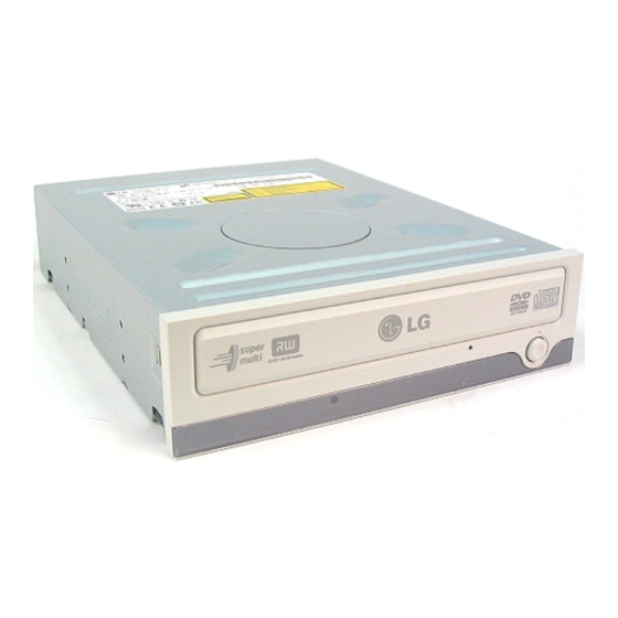
LOCATION OF CUSTOMER CONTROLS Front Panel Emergency Eject Hole Disc Tray Eject Button Drive Activity Indicators NOTE: The actual drive may be different from this design. 1. Disc tray 3. Emergency Eject Hole This is the tray for the disc. Place the disc on the Insert a paper clip here to eject the Disc tray ejected disc tray, then lightly push the tray (or manually or when there is no power. - Page 10 Rear Panel IDE Interface Connector Analog Audio Output Connector Jumper Connector Power Connector Digital Audio Output Connector NOTE: The actual drive may be different from this design. 1. Power Connector 3. Jumper Connector Connects to the power supply (5-and 12-V DC) of This jumper determines whether the drive is the host computer.
-
Page 11: Disassembly
DISASSEMBLY 1. CABINET and CIRCUIT BOARD 1-3. Cabinet and Main Circuit Board A. Remove the Cabinet in the direction of arrow (4). DISASSEMBLY (See Fig. 1-3) 1-1. Bottom Chassis B. Release 2 hooks (a) and remove the CD Tray A. Release 4 screws (A) and remove the Bottom Chassis drawing forward. -
Page 12: Pick-Up
2-2. Pick-up A. Release 1 screw (C) and remove the Pick-up. Pick-up Unit Pick-up Fig. 2-2... -
Page 13: Exploded View
EXPLODED VIEW PBM00 (MAIN C.B.A) PBF00 (FRONT C.B.A) -
Page 14: Glossary
GLOSSARY ATIP Absolute Time in Pre-groove. With an additional modulation of the “Wobble”, the “Groove” contains a time code information. Wobble The pre-groove in the Disc is not a perfect spiral but is wobbled. With : – A typical amplitude of 30 nm –... -
Page 15: The Differences Of Cd-R/Cd-Rw Discs And General Cd-Rom
The differences of CD-R/CD-RW discs and General CD-ROM 1. Recording Layer Recordable CD has a wobbled pre-groove on the surface of disc for laser beam to follow track. Track pitch(p) a=30nm Read-only Disc CD-ROM (READ-ONLY DISC) Radial Direction Radial Error Signal 0.4~0.5 um Groove Land... -
Page 16: Disc Materials
3. Disc Materials 1) CD-ROM disc • It is composed of Silver _ colored aluminum plate and Reflective layer. • Groove (Pit) of aluminum plate make a track. • Laser wavelength : 780 nm, Laser Power (Read): 0.5mW • Signal is detected by the difference of reflective beam intensity between “pit”... -
Page 17: Reading Process Of Optical Disc
3) CD-RW Disc Label Printing Protective Layer Dielectric Layer(TL) Recording Layer Dielectric Layer(UL) Substrate (Polycarbonate) Groove Laser Beam • It is composed of polycarbonate layer, alloy(silver, arsenic) layer, aluminum reflectivity layer, protective layer. • An crystalized alloy layer is transformed into noncrystalized by the laser heat. Therefore, writing and reading is enabled by the difference of reflectivity. -
Page 18: Writing Process Of Cd-R Disc
5. Writing Process of CD-R Disc Incident (Write) Laser Power (Read) (Read) Laser Spot a b c d e f Position (Time) Laser Below "ORP"– Mark Too Short Spot Reflected At Optimum Record Power ("ORP") Light Signal Above "ORP" – Mark Too Long Recorded Mark Time... -
Page 19: Organization Of The Pca, Pma And Lead-In Area
7. Organization of the PCA, PMA and Lead-in Area 1) Layout of CD-ROM disc Disc Center Diameter 120 mm Diameter 46 mm Diameter 15 mm Center hole Clamping and Label Area Information Area Read Only Disc Lead-in Area Program Area Lead-out Area 2) Layout of CD-R/RW disc Disc Center... -
Page 20: Function Of Pca And Pma Area
8. Function of PCA and PMA area 1) PCA (Power Calibration Area) • PCA area is used to determine the correct Laser Power for a disc. – Method 1 : PCA area is divided by a track. – Method 2 : The previous Calibration value is referred. –... -
Page 21: Writing Process Of Disc
2) ROPC (Running Optimum Power Control) • Variable primary factor of Optimum Power – Change of Power sensitivity on the Disc. (limited to 0.05 *Po) – Wavelength shift of the laser diode due to the operating temperature change. – Change of the Spot aberration due to the Disc skew, Substrate thickness, Defocus. -
Page 22: The Differences Of Dvd-R/Rw, Dvd+R/Rw Discs And Dvdd-Rom
The differences of DVD-R/RW, DVD+R/RW discs and DVD-ROM 1. Recording Layer DVD-ROM (Read Only Disc) 0.4 um DVD-R/RW Disc (Land Pre-Pit) DVD+R/RW Disc... -
Page 23: Disc Specification
2. Disc Specification DVD-ROM DVD-R DVD-RW DVD+R DVD+RW Single-Layer Dual-Layer Media Type Read Only Read Only Phase change Phase change 4.7GB 8.54GB 4.7GB 4.7GB 4.7GB 4.7GB User data capacity Wavelength 650nm 650nm 650nm 650nm 650nm 650nm Reflectivity 45~85% 18~30nm 45~85% 18~30% 45~85% 18~30nm... - Page 24 2) Recording format using organic dye material (DVD-R/DVD+R) * The format that records data through the creation of recorded marks by changing the organic dye material with a laser beam. > Disc structure DVD-R DVD+R Adhesive layer Adhesive layer Protective layer Protective layer Reflective layer Reflective layer...
- Page 25 3) Recording format using phase-change recording material (DVD-RW/DVD+RW) * Data is recorded by changing the recording layer from the amorphous status to the crystalline status, and played back by reading the difference of the reflection coefficient. [ Amorphous : Non-crystalline ] >...
-
Page 26: Writing Pulse Waveform Of Dvd+R
4. Writing Pulse Wave Form of DVD+R For different speed ranges, different write strategies can be used. This document specifies 2 options: - a pulsed write strategy, where each single mark is created by a number of subsequent separated short pulses. - Page 27 2) 2 Method : Using Blocked Write Strategy NRZI Channel bits 1.25T top,3 1.25T 3T mark top,3 top,4 1.25T 4T mark top,4 1.25T 5T mark top,4 1.25T Etc. top,4 N = 3 : T (cm = 3) can be optimized individually. N >...
-
Page 28: Writing Pulse Waveform Dvd+Rw
5. Writing Pulse Wave Form of DVD+RW NRZI Channel bits Ttop dTera dTtop Pp : Actual write power Pe : Erase Power Pb : Bias Power... -
Page 29: Organization Of Inner Drive Area, Outer Drive Area, Lead-In Zone And Lead-Out Zone
6. Organization of the Inner Drive Area, Outer Drive Area, Lead-in Zone and Lead-out Zone 1) Layout of DVD-ROM disc Disc Center Diameter 120 mm Diameter 44 mm Diameter 33 mm Diameter 22 mm Diameter 16 mm Diameter 15 mm Clamping Center 3rd transtion... - Page 30 3) Layout of DVD+RW disc Disc Center Diameter 120 mm Diameter 44 mm Diameter 33 mm Diameter 22 mm Diameter 16 mm Diameter 15 mm Clamping Center 3rd transtion Information Zone Zone hole area 1st transition area Rim area 2nd transition area Unrecorded Disc Lead -out Zone Lead-in Zone...
-
Page 31: Dvd & Cd Data Processing
DVD & CD DATA PROCESSING 1. Data Processing Flow... -
Page 32: Copy Protection And Regional Code Management Block
2. Copy Protection and Regional Code Management Block Block Diagram Change the "KEY" HOST DVD R8J32006FP PLAYER (EMPEG2 B/D) Scrambled MPEG Data KEY Management Control Brief Process 1. Regional Code for DVD Disc – DVD-ROM drive transfers the regional code of the control data to host by the command of host, the DVD player of host reads the regional code, and plays title in the case of allowed regional code only. -
Page 33: About Prevention The Dvd-Rom From To Be Copy
3. About Prevention the DVD-ROM from to be copy A data is able to encode and record in the disc, if a copyright holder wants to prevent the disc from copying. In case of a disc enhanced movie of 3 titles..DISC KEY (2048 Bytes) is used to encode the whole contents in the disc and TITLE KEY (5 Bytes) is used to encode the title respectively. -
Page 34: About The Dvd-Rom Regional Code
4. About the DVD-ROM Regional Code Regional code U.S.A PRI. VIR DISC ROM - DRIVE MPEG-2 BOARD VGA CARD MONITOR Transfer to Receiving If the board is setting to the regional The disc has MPEG-2 board data from the code 1 for the U.S.A..the regional reading the MPEG-2... -
Page 35: Internal Structure Of The Pick
INTERNAL STRUCTURE OF THE PICK-UP 1. Block Diagram of the PICK-UP(HOP-7532TS) Tilt- 44 Tilt+ 43 TR- 42 TR+ 41 AF- 4700p 4.7k 40 AF+ R2 1.5k 39 GND(LDD) R4 360k(1%) 16 15 14 13 12 11 10 38 ENA 37 SLG CD LD 36 IAPC C2 0.1u... -
Page 36: Pick Up Pin Assignment
2. Pick up Pin Assignment Signal Name Signal Description GND(OEIC) Ground for OEIC Vcc(OEIC) Power supply for OEIC(+5V) Vc(OEIC) Reference voltage input for OEIC(+2.3V) GAINSW OEIC output gain control (High:Low gain, Middle:Middle gain, Low:High gain) E3+F3 Single OEIC output EF3 Single OEIC output B Single OEIC output D E4+F4... -
Page 37: Signal Detection Of The P/U
3. Signal detection of the P/U Infrared Iaser Pick-Up module Focusing Tracking Photo Diode 1) Focus Error Signal ==> (A+C)-(B+D) This signal is generated in RF IC (IC101 : HD153724TF) and controls the pick-up’s up and down to focus on Disc. 2) Tracking Error Signal (DPP Method) ==>... -
Page 38: Description Of Circuit
DESCRIPTION OF CIRCUIT 1. ALPC (Automatic Laser Power Control) Circuit 1-1. Block Diagram... - Page 39 1-2. ALPC (Automatic Laser Power Control) Circuit ALPC function DVD/CD anlaog front-end IC(IC101 HD153724TF) is for constant power control purpose. Based on the accurate power sensor(FMON) in P/U, ALPC feedback loop maintains constant power level against laser diode’s temperature variation. The ALPC loop amplifies(10x) the FMON signal to enhance the accuracy of read power level control.
-
Page 40: Focus Circuit
2. Focus Circuit 2-1. Block Diagram A+B+C+D HAVC A,B,C,D 0.8V IC101 HD153724TF HAVC A,B,C,D (EF1~EF4) R334 Disc (A+C)-(B+D) Optical (A+C)-(B+D)+K[(EF1+EF3)-(EF2+EF4)] Motor unit Pick-up C325 HOP-7532TS Focusing Compensator IC301 FACT- FACT+ R8J32006FP R346 FOIN FACT+ C338 FACT- IC601 1.65V R2S30200FP CTL1 CTL2 2-2. -
Page 41: Tracking & Sled Circuit
3. Tracking & Sled Circuit 3-1-1. Block Diagram (Tracking Following) IC101 HD153724TF MPPO (A+D)-(B+C) HAVC SPPO A,B,C,D (EF1~EF4) Disc R337 Optical (A+D)-(B+C)-K[(EF1+EF4)-(EF2+EF3)] Motor unit Pick-up HOP-7532TS C328 Tracking Compensator TACT- TACT+ Sled IC301 Compensator R8J32006FP SLED MOTOR Unit R348 TOIN TACT+ IC601 C339... - Page 42 3-1-2. Block Diagram (Seek) IC101 HD153724TF MPPO (A+D)-(B+C) HAVC SPPO (EF1~EF4) A,B,C,D [(EF1+EF4)-(EF2+EF3)] Disc Optical VREF1 C114 Motor unit Pick-up A+B+C+D HOP-7532TS TEIN VREF1 TACT- TACT+ HAVC MIRR MIRR SUMF BOTTOM RFIP HOLD HOLD SLED MOTOR RFIN Unit MIRRTOPH MIRRBOTH C136 C137 C328...
- Page 43 3-2-1. Tracking Servo The aim of tracking servo is to make laser beam trace the data track on disc. Tracking Error(TE) Signal is generated from tracking error detected block in HD153724 using DPP(Differential Push-Pull) Method and DPD (Differential Phase Detection) Method. DPP Method uses not only main beam(A, B, C, D) but also side beam(EF1~EF4) for correcting DC offset generated in Push-Pull Method.
-
Page 44: Spindle Circuit
4. Spindle Circuit 4-1-1. Block Diagram(FGCAV Servo) Optical Pick-up HOP-7532TS Disc Motor unit X301 33.8688MHz VCK4M IC301 Control Clock R8J32006FP Generator CAV FD R330 CAV PD VCK4M R326 R329 Motor Kick 3.3V C319 1.65V SPIN IC601 DAVC 1.65 R2S30200FP CTL1 CTL1 CTL2 CTL2... - Page 45 4-2-1. Block Diagram (Wobble CLV Servo) C119 C120 C121 WAG1 WAG2 WAG3 21 22 AGC1 AGC2 Disc Motor uni t Optical Pick-up AGC3 HOP-7532TS WOBSIG WBLSH IC101 WBLSH VREF HD153724TF IC301 R8J32006FP 1.65V R329 R330 C319 Motor Kick 1.65V 4-2-2. Wobble CLV Servo DVD-RAM: 2x, 3x, 5x / DVD-R: 16x(PCAV), 8x, 4x, 2x / DVD+R: 16x(PCAV), 8x, 4x, 2.4x / DVD-RW: 1x, 2x, 4x, 6x / DVD+RW: 2.4x, 4x, 8x...
-
Page 46: Major Ic Internal Block Diagram And Pin Description
MAJOR IC INTERNAL BLOCK DIAGRAM AND PIN DESCRIPTION IC101 (HD153724TF) : RF AMP Analog Signal Processor Pin Assignment SUMF/SUMF2 RFIP MCLK RFIN IP1/LPPOUT SRVREF IP2/MIRR FVREFO WOBSIG IREFT RDGATE VREF1 LO_ZB/SPDSH HAVC IDGATE RFHLD/TISH1 HD153724TF BLANK PWDETO (TOP VIEW) GND4 (3.3V)VDD2 RLDON WGATE... - Page 47 Block Diagram *3300p *3300p/0.1u Lo-Z Function by IDGATE VREF1 fast mode „ = 3.3us 0.47u *3300p/0.068u (*2) 4700p (Ri=1k/20k switch) molk to MIRR DEFECT 0.068u RFIP EQOP RF SUM/SUB RFIN EQON SUBP,N (RGA) AUTO 0.068u SUMF2 EQOS to WRF IP1/LPPOUT ATEST LPPMON/EQOS/RRF/WRF IP2/MIRR...
- Page 48 • Pin Description Pin no. Pin Name Type Function Not connected Analog-Output Lens error signal output terminal Not connected Analog-Output Focal error output terminal Analog-Output PE output terminal Analog-Output Tracking error output terminal TEIN Analog-Input TZC detecting TE signal input terminal SIGM Analog-Output Analog signal monitoring output terminal...
- Page 49 Pin no. Pin Name Type Function BLANK Digital-Output Record/non-record detecting output terminal / BD detecting output terminal. RFHLD/TISH1 Digital-Input RF hold control signal input terminal / Tilt servo detecting sampling pulse input terminal. IDGATE Digital-Input ID Select pulse input terminal. LO_ZB/SPDSH Digital-Input Low-z (reversal) pulse input terminal / Pickup input...
- Page 50 Pin no. Pin Name Type Function AGHPF2 External-capacitor required Terminal to connect AGC high pass filter capacitor. AGHPF1 External-capacitor required Terminal to connect AGC high pass filter capacitor. AGFU External-capacitor required AGC filter connecting terminal. AGFR External-capacitor required AGC filter connecting terminal. VCC1 Power Power supply connected terminal(5V).
- Page 51 IC301 (R8J32006FP) : Encoder, Decoder & DSP Singal Processor 1.1 Pin Layout VSSR DOUT VCCI0 VCCR VSSI0 MRSTB TESTB1 IOCS16B VSSRQ HINTRQ TESTB2 DACKB TEST0 IORDY VCCRQ ZIORB TEST1 ZIOWB TEST2 DREQ TEST3 DATA15 VSSRQ DATA0 HEATRUN DATA14 CSEL DATA1 AMUTE VCCI0 VCCI0...
- Page 52 1.2 Block Diagram VREF, VREFC VREF33 BIAS VIBIAS LOUT AUDIO ROUT EFMP AUDIO DOUT EFMN Data DFF[1:0] DREQ Slicer JFF[1:0] DACKB CD-ROM DASPB Descramble DCLPF[2:0] Decoder CS3FXB Data DRLPF[2:0] CS1FXB Strobe VISTRB PDIAGB MONANA[1:2 ATAPI W1LPF[2:0] CD-DSP Scramble WPLL Jitter IOCS16B W2LPF[2:0] Counter...
- Page 53 1.3 Pin Table Pin No. Pin Name Pin No. Pin Name Pin No. Pin Name Pin No. Pin Name VSSR LOADOUT SDATA DCLK DOUT LOADIN SCLK VCCA VCCR VSSRQ FEMCK VCCA EJECTSW RDGATE MRSTB ACTFLG LOWZB TESTB1 DRVEN1 IDGATE SIGM VSSRQ VCCRQ RFHLD...
- Page 54 Pin No. Pin Name Pin No. Pin Name Pin No. Pin Name Pin No. Pin Name VCCA DATA7 PDIAGB W1LPF2 DATA8 W1LPF1 DATA6 W1LPF0 DATA9 CS1FXB CPU15 VSSA DATA5 CS3FXB CPU14 VREFC DATA10 DASPB CPU13 VIBIAS DATA4 UCS1B CPU12 VREF DATA11 UCS0B CPU11...
- Page 55 1.4 Pin Functions It corresponds to the following signs as a pin I/O specification. AI : Analog Input IOU : Standard Input/Output with Pull Up AO : Analog Output 5I : 5V Tolerant Input AIO : Analog Input/Output 5O : 5V Tolerant Output Standard Input 5TO : 5V Tolerant Three State Output...
- Page 56 1.4.2 Servo Pin List Pin Name Pin No. Destination Function DEFECT Defect (scratch detect) signal BLANK Blank signal input (also connected to the H8S interrupt port INT5) Tracking Zero Crossing signal input DRVR Spindle FG pulse (also input to the H8S interrupt port INT4) DRVR Tilt drive signal (PWM output) DRVR...
- Page 57 1.4.3 ATAPI Interface Pin List Pin Name Pin No. Destination Function HRSTB ATAPI ATAPI- IF control signal (host reset signal) ATAPI ATAPI- IF register address signal DATA[15:0] 180, 178, ATAPI ATAPI- IF data bus 172, 170, 168, 166, 164, 162, 161, 163, 165, 167, 169, 171,...
- Page 58 1.4.4 Encoder Interface Pin List Pin Name Pin No. Destination Function IP1LPPIN PID area identification signal/LPP input signal IP2MIRR PID area identification signal/MIRR signal WOBSIG Wobble signal input LSRERR Laser error signal RDGATE PLL input switch signal LOWZB Input impedance switch control signal/SPDSH; running OPC sampling pulse (Pit top) IDGATE ID/data switch signal...
- Page 59 1.4.5 Serial Communication Interface Pin List Pin Name Pin No. Destination Function LDBUSY LDD serial IF busy microcomputer I/F (transfer enable signal) LDD2 SCK(WDEN2) LDD2 microcomputer I/F (transfer enable signal) RFDEN AFE/LDD microcomputer I/F (transfer enable signal) SDATA AFE / LDD AFE/LDD microcomputer I/F (transfer data signal 3V system) SCLK...
- Page 60 1.4.8 H8S Micro-Processor Pin List (a) CPU Pin Name Pin No. Destination Function HEATRUN ATAPI CPU general port 1- 0: Off heat run test input CSEL ATAPI CPU general port 1- 6: ATAPI CSEL AMUTE Audio Mute ckt CPU general port 0- 2: Audio mute CSW3 CPU general port 1- 7: Cartridge detect signal 3 CSW2...
- Page 61 (b) Flash/SRAM Pin Name Pin No. Destination Function UCS1B SRAM H8S/CS1, also functions as the CPU general port 2- 0 UCS0B Flash H8S/CS0 CPWRB Flash/SRAM H8S/WRB CPRDB Flash/SRAM H8S/RDB A[20] Flash/SDRAM H8S/A[20] A[19:17] 204, 205 H8S/A[19:17] A[16:0] 207, 208 H8S/A[16:0] 209, 210 211, 212 215, 216...
- Page 62 1.4.9 LSI/TEST Control Pin List Pin Name Pin No. Destination Function ROMICE Non-maskable CPU interrupt port (sensed at the falling edge) MRSTB RESET IC Master reset input TESTB1 Test select TESTB2 TEST0 User test/CPU general port 2 TEST1 Test monitor can be set as the following table by a register.
- Page 63 1.4.10 Power Supply/GND Pin List Pin Name Pin No. Function 32, 53, DSP core power supply (1.5V) 173, 188, VCCR 3, 62 SDRAM power supply (3.3V) VCCRQ 10, 23, SDRAM I/O power supply (3.3V) 31, 39. VDDAA 1.5V system analog power supply (1.5V) WPLL1, 2 VCCA Analog power supply (3.3V) : Dedicated for LVDS Analog power supply (3.3V) : Servo A/D...
- Page 64 IC601 (R2S30200FP) : SPINDLE MOTOR AND 6CH ACTUATOR DRIVER Pin Layout R2S3 0200FP Package outline : 42 PIN POWER SSOP (42P9R-K) Pin Function No Pin name Function Pin name Function SPIN Spindle control voltage input Reference voltage input SL1IN Slide control voltage input1 LOIN Loading control input SL2IN...
- Page 65 Block Diagram...
- Page 66 Input/Output circuit diagram SPIN, SL1IN, SL2IN FOIN, TOIN, TLIN EN1, EN2 LOIN OPIN- 5VCC 5VCC 5VCC 5VCC SLGS ACTFLG, FG ACTRST OPOUT 5VCC (Temperature monitor) 5VCC 5VCC 5VCC 5VCC 5VCC 5VCC VM1, U, V, W VM2, SL1+, SL1-, SL2+, SL2- SL1+ SL1- SL2+...
-
Page 67: Troubleshooting Guide
TROUBLESHOOTING GUIDE (01) Laser Power Adjust (using RD Power/WR Power/Erase Power) MPU & DSP IC301 Pickup Setting Pin#106 pin#112 Front Monitor Driver IC101 IC201 (02) High Frequency/NRZI skew Adjust Pickup 21-24 MPU & DSP Driver IC301 (03) Data Slice/Equalizer Boost/Raw Slice/ Equalizer Frequency Adjust Pin#76 MPU &... - Page 68 (06) Focus Amp. and Total Amp. Adjust All Disc Setting Pin# Pickup 85-98 FE:R334,C325 IC101 MPU & DSP IC301 PE:R335,C326 Focus:#34-35 R346, Driver C338 IC601 (07) Tracking Amp. Adjust All Disc Setting Pin# Pickup 85-98 IC101 TE:R337,C328 MPU & DSP IC301 Tracking #30-31...
- Page 69 (09) Unwritten Slice Level Adjust for DVD-RAM DVD-RAM Disc Pin# Setting 77-78 IC101 Pickup MPU & DSP IC301 SIGM:R336, C327 #102 Slider FPC Slider:#6, 8-10 Driver IC601 (10) Focus Offset Adjust for DVD-ROM, CD-R/RW DVD-ROM Disc Pin# 85-98,77-78 Setting IC101 MPU &...
- Page 70 (13) Tilt Adjust for DVD-RAM DVD-RAM Disc Pin# Setting Pickup 85-98,77-78 IC101 TCE:R340, C331 MPU & DSP IC301 TIE:R341,C333 Slider FPC Driver Slider:#6, 8-10 IC601 (14) Tilt Adjust for DVD-R/RW, DVD+R/RW, CD-R/RW DVD-R/RW Disc Pin# Setting 85-98, 77-78 IC101 TE:R337, C328 MPU &...
- Page 71 (17) Lens Sensitivity Adjust Pickup MPU & DSP (Temp.Information) #113 IC301 (18) Spindle Offset Adjust Pin# Spindle 12-14 Driver MPU & DSP IC601 IC301 SPD:R330,C319 (19) ADIP BPF/Read Timing Adjust for DVD+R/RW DVD+R Disc Setting Pin# 85-98,77-78 IC101 Pickup MPU & DSP WobSIG IC301 #46 #46...
- Page 72 (21) RTZ TimeOut Fail & Slider/ Slider FPC Driver Spindle Slider:#6,8-10 IC301 IC601 Spindle FFC (22) Focus Servo/Tracking Servo Fail All Disc Pin# Setting 85-98 IC101 FE:R334,C325 Pickup MPU & DSP IC301 TE:R337,C328 Focus:#34-35 Tracking:#30-31 PE:R335,C326 R346,C338 Slider FPC Driver Slider:#6,8-10 IC601 R348, C339...
- Page 73 Detail Error Code & Fail Analysis 1. Laser Power Initial Adjust Error Code Contents of fail Fail Analysis Block Diagram SSB Byte8,9 28xx LP Adjust NG. 1) Check Pickup FFC Connection. No.01 (Exchange 2) Check solder of IC101circumference. low/high byte) (pin#10, 14, 16, L150, L151) 3) Check solder of IC201.
- Page 74 2. Adjusting Error during Disc Load Sequence (Lead in Error) No. Error Code Contents of fail Fail Analysis Block Diagram SSB Byte21,22 42xx Circuit Offset Adjust NG. 1) Check Pickup FFC Connection. No.04 2) Check solder of IC101circumference . (pin#,4,5,6 pin#85-98, FE_Servo: R334, C325 TE_Servo: R337, C328 PE_Servo: R335, C326)
- Page 75 No. Error Code Contents of fail Fail Analysis Block Diagram SSB Byte21,22 4Axx Focus Offset Adjust NG. 4A08: Disc Unmatch(Exchange Disc). No.10 (DVD-ROM,CD-R/RW) 1) Check Pickup FFC Connection. 2) Exchange Pickup. 3) Exchange IC301(MPU & DSP). 4A5x Focus Offset Adjust NG. 1) RAM Disc NG (Exchange RAM Disc) No.11 4A6x...
- Page 76 No. Error Code Contents of fail Fail Analysis Block Diagram SSB Byte21,22 54xx DPP Amp Adjust NG. 1) Check Pickup FFC Connection. No.07 (CD Disc Only) 2) Exchange Pickup. 3) Check solder of IC101circumference. (pin#4,5,6 pin#85-98, TE_Servo: R337, C328) 4) Exchange IC101(AFE). 5) Exchange IC301(MPU &...
- Page 77 No. Error Code Contents of fail Fail Analysis Block Diagram SSB Byte21,22 5Axx ADIP read timing Adjust NG. 5A01: Check DVD+R Disc (Exchange Disc) . No.19 1) Check Pickup FFC Connection. 2) Exchange Pickup. 3) Exchange IC101(AFE). 4) Exchange IC301(MPU & DSP). 5) Exchange IC601(Driver) 5Cxx Signal Amp Error.
- Page 78 3. Loading Sequence Error (Lead in Error) No. Error Code Contents of fail Fail Analysis Block Diagram SSB Byte21,22 2503,2504 RTZ Timeout(Sled Timeout). 1) Check Slider FPC Connection. No.21 2) Check solder of IC601 circumference . (pin#2-3, 6, 8-10) 3) Exchange IC601. 4) Exchange Slider Motor.
- Page 79 Power Supply System Diagram NTMT L601 DRV IC601 R2S30200FP VM1 #22 Motor power supply 1(Spindle) SW701 VM2 #05 Motor power supply 2(Slide) ROHM BD9703FP S711 S711 IC702 LDD CN101 5.3V VSO(5.3) 5VDC/DG IMSY-CNT-N45PO Pickup 5-ELCO-JR5 Converter OPEN OPEN VSO #13 Vin=12.00V Vo=5.30V L602...
- Page 80 PCB Poor Analysis - Check list Circuit/IC Signal Signal/Level mesurement-point (IC-pin or Device) Power supply Line-12V CN801-41 Line-5V CN801-44 (IC701) reg-1.5V 1.5V IC701-2 reg-2.8V 2.8V IC701-5 (IC702) reg-5.3V 5.3V TP714 (IC703) reg-3.3V 3.3V IC703-2 Flash-ROM VDD : 3.3V 3.3V (IC302) Active-Low read-CK VDD : 1.5V...
- Page 81 HW Self- Diagnostic function 1. Self-Diagnostic Function by LED Blink. • Basic operation: At JR5, MPU is included in DSP, MPU accesses each peripheral (inside, exterior) device, and discover a defect by the ability of a read/write of data to be performed correctly. Since MPU operates by the program with a built-in Flash-ROM, when abnormalities are in MPU, Flash-ROM, and these Data-Bus &...
- Page 82 2. LED does not blink at all at the time of a power supply injection. Eject-SW does not react. (1) Is it normal to the exterior Bus (Data-Bus, Address-Bus, control signal system) of MPU? Viewing — check: -- a short circuit, opening, etc. •...
- Page 83 3. Motor, Abnormalities in Actuator System The drive circuit of a motor & actuator consists of the three ICs IC601(R2S30200FP). The work of each IC is as follows. (1) IC601(R2S30200FP) : 7ch driver Spindle motor driver: 180° audio drive Type, an analog input, a PWM drive, a Vm=12V. Stepping motor driver X2: analog input, a PWM drive (differential), a Vm=12V Loading motor driver: Input/Output PWM drive, Vm=5V.
-
Page 84: Block Diagram
BLOCK DIAGRAM Flash-ROM (2MByte) MBM29LV160BE OPU:HOP-7532TS or Equivalent (HITACHI ME) (FUJITSU) Disc Interface Loading motor connector Analog Front End DVD/CD DSP Analog HD153724TF (DVD/CD/Servo/ATAPI) audio Disc R8J32006FP 100pin-TQTF Slide motor 256pin LQFP motor (RENESAS) Unit (RENESAS) mechanism DVD-codec Host IDE CD-codec LPP/ADIP decorder 7ch-Driver...
Need help?
Do you have a question about the GSA-4163B and is the answer not in the manual?
Questions and answers