Table of Contents
Advertisement
Mar. 2012
Table of Contents
Cautionary Notes ..............................................................2
Specifications .....................................................................2
Location of Controls .........................................................4
Location of Controls Parts List........................................5
Exploded View ..................................................................6
Exploded View Parts List.................................................8
Wiring Diagram/Block Diagram..................................10
Parts List ...........................................................................12
Verifying the Version......................................................14
Data Backup and Restore Operations ..........................14
Performing a Factory Reset............................................14
Updating the System ......................................................15
Copyright © 2012 Roland Corporation
All rights reserved. No part of this publication may be reproduced in any form without the written permission
of Roland Corporation.
Test Mode .........................................................................16
Additional Tests ..............................................................21
Circuit Board (Main Board) ...........................................22
Circuit Diagram (Main Board: CPU) ............................24
Circuit Diagram (Main Board: Analog) .......................26
Circuit Diagram (Main Board: Power) .........................28
Circuit Diagram (Main Board: Digital) ........................30
Circuit Board (Panel, Jack, EXP Board) ........................32
Circuit Diagram (Panel Board)......................................34
Circuit Diagram (Jack Board) ........................................36
Circuit Diagram (EXP Board) ........................................37
17058788E0
SERVICE NOTES
Issued by RJA
GT-100
CC-KWS
Advertisement
Table of Contents

Related Manuals for Boss GT-100


Summary of Contents for Boss GT-100
-
Page 1: Table Of Contents
Mar. 2012 GT-100 SERVICE NOTES Issued by RJA Table of Contents Cautionary Notes ..............2 Test Mode .................16 Specifications ..............2 Additional Tests ..............21 Location of Controls ............4 Circuit Board (Main Board) ...........22 Location of Controls Parts List........5 Circuit Diagram (Main Board: CPU) ......24 Exploded View ..............6... -
Page 2: Cautionary Notes
* AF method (Adaptive Focus method) Back Up User Data! This is a proprietary method from Roland & BOSS that vastly improves the signal-to-noise (S/N) ratio of the A/D and D/A converters. User data may be lost during the course of the procedure. Refer to “Data Backup and Restore Operations”... - Page 3 INPUT: -10 dBu Footswitch: BOSS FS-5U RETURN: -10 dBu Dual Footswitch: BOSS FS-6 AUX IN: -20 dBu Expression Pedal: BOSS FV-500L/500H, Roland EV-5 Input Impedance INPUT: 1 MΩ RETURN: 100 kΩ AUX IN: 47 kΩ * 0 dBu = 0.775 Vrms * Printed matters will not be supplied after the end of the production.
-
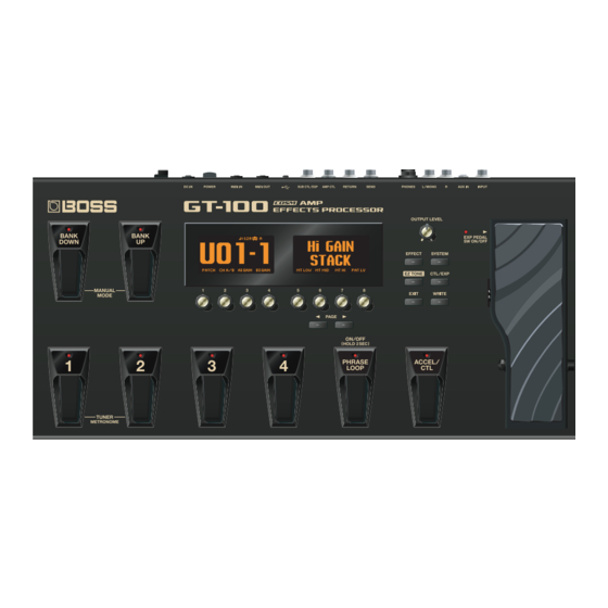
Page 4: Location Of Controls
Mar. 2012 GT-100 Location of Controls fig.panel.eps... -
Page 5: Location Of Controls Parts List
Mar. 2012 GT-100 Location of Controls Parts List Part Code Part Name Description Q’ty 5100024857 TOP COVER 5100024861 DISPLAY COVER 5100027738 PE13264ORT-006I03Q 5100025466 SW PEDAL ESCUTCHEON 5100001928 SW PEDAL (G2187916R0) 03344723 TACT SWITCH SKQKAKD010 5100024880 PEDAL LABEL (BANK DOWN) 5100024879... -
Page 6: Exploded View
Mar. 2012 GT-100 Exploded View fig.bunkaizu-e.eps@L Indicator present No indicator present... - Page 7 Mar. 2012 GT-100 fig.bunkaizu-e.eps@R...
-
Page 8: Exploded View Parts List
Mar. 2012 GT-100 Exploded View Parts List Parts Part Code Part Name Description Q’ty 5100024146 MAIN BOARD ASSY 5100024147 PANEL SHEET ASSY * This unit includes the following parts. ******** PANEL BOARD ******** JACK BOARD ******** EXP BOARD 5100024857 TOP COVER... - Page 9 Mar. 2012 GT-100...
-
Page 10: Wiring Diagram/Block Diagram
Mar. 2012 GT-100 Wiring Diagram/Block Diagram fig.wiring-block.eps@L Part Code Part Name Description Q’ty 5100026016 WIRING W1(INPUT-OUTPUT) 5100026017 WIRING W2(EXP) 5100026033 WIRING MLC 1.25-26X90-01... - Page 11 Mar. 2012 GT-100 fig.wiring-block.eps@R...
-
Page 12: Parts List
Mar. 2012 GT-100 Parts List fig.-part1-e.eps Due to one or more of the following reasons, Safety Precautions: parts with parts code ******** cannot be supplied as service parts. The parts marked have safety-related characteristics. Use only listed parts for replacement. - Page 13 Mar. 2012 GT-100 SCREWS 40017934 SCREW M3X6 PAN MACHINE W/SW+PW(L) FE ZC 40342712 SCREW M3X6 PAN MACHINE W/SW+SMALL PW BZC 5100002092 SCREW M6X70 (H5029867R0) HEX BOLT HALF THEREAD BZC 40233012 SCREW 2.6X8 BINDING TAPTITE P BZC 40019123 SCREW 3X8 BINDING TAPTITE S BZC...
-
Page 14: Verifying The Version
RECEIVING... is displayed on the GT-100’s LCD screen. If nothing is suitable value. received, verify that the GT-100’s device ID is the same as when the bulk dump was performed. When the receipt of data ends, the BULK DATA RECEIVING... message Items Required disappears. -
Page 15: Updating The System
Adjust the OUTPUT LEVEL knob to minimum. Hold down SYSTEM and press and hold POWER. * Do not connect the GT-100 and the computer yet. The unit’s on-board updater starts, and a display like the one shown below appears on the LCD screen. -
Page 16: Test Mode
* If the message PROGRAM: USER NG is displayed, a factory reset must be Using the USB cable, connect the GT-100 and the computer. executed. (Refer to Performing a Factory Reset (p. 14).) Connect the EV-5 to the SUB CTL 1,2/SUB EXP connector. - Page 17 Mar. 2012 GT-100 3. LCD Verify that all on-screen dots have become brighter. fig.lcd-dot.eps A screen for adjusting the backlight brightness appears on the left and right LCD screens. fig.lcd-backlight.eps 10. Press PAGE 11. Verify that only the outermost periphery of the screen has become brighter.
- Page 18 Mar. 2012 GT-100 8. EXTERNAL EXP Connect the oscilloscope to the PHONES connector, and verify that the output values are as shown below. Depress the heel of the EV-5, and verify that the message MIN: OK PHONES L: 6.5 Vpp–7.5 Vpp appears on the left screen.
- Page 19 Mar. 2012 GT-100 AUX IN -> OUTPUT L/MONO and R (-10 dB Mode) Depress CTL/EXP. A screen like the one shown below is displayed. Signal Levels fig.audio-1.eps Connect the signal generator to the AUX IN connector, and input the following signal.
- Page 20 Mar. 2012 GT-100 RETURN -> SEND (Signal Levels) RETURN -> SEND (Residual Noise) Set the GND LIFT switch to GND. Connect the 1/4-inch phone plug equipped with 47-kΩ load resistor to the RETURN connector. Connect the signal generator to the RETURN connector, and input the following signal.
-
Page 21: Additional Tests
Verifying Current Consumption Connect the DC IN current-consumption measurement cable to the DC IN connector on the GT-100, then connect the AC adaptor. fig.connect-cable.eps Press WRITE again. A screen like the one shown below appears and the factory reset starts. -
Page 22: Circuit Board (Main Board)
Mar. 2012 GT-100 Circuit Board (Main Board) fig.b-main-1.eps... - Page 23 Mar. 2012 GT-100 fig.b-main-2.eps...
-
Page 24: Circuit Diagram (Main Board: Cpu)
Mar. 2012 GT-100 Circuit Diagram (Main Board: CPU) fig.d-main-2.eps@L AMP-CTL XLCD-RST XCODEC-PDN XPWR-OFF XOUTPUT-MUTE D+3.3 OUTPUT-GAIN JTAG for ESC2 XSF-WP R117 D+3.3 EXB28V220JX EXB28V330JX R133 EXB28V220JX MA(15) XICE-RST AA15 RA11 MA(14) EXB28V330JX MA(12) D+1.2 MA(11) AA14 RA12 MA(10) 14FMN-BMTTN-A-TF (LF)(SN) - Page 25 Mar. 2012 GT-100 fig.d-main-2.eps@R D+1.2 C115 C109 C111 C113 0.1uF 47uF 10uF 10uF C116 2125 2125 0.1uF C117 MA(15:0) 0.1uF C118 MD(15:0) 0.1uF C119 0.1uF C120 0.1uF D+3.3 MD(15) UnPop DQ15 MA(14) RA38 MD(14) DQ14 MA(15) EXB28V470JX MD(13) DQ13 R190...
-
Page 26: Circuit Diagram (Main Board: Analog)
Mar. 2012 GT-100 Circuit Diagram (Main Board: Analog) fig.d-main-3.eps@L C215 UnPop R221 D ( 0.5% ) R219 D ( 0.5% ) C225 UnPop NJM4580M(TE3) R224 TP327 TP328 D ( 0.5% ) R222 D ( 0.5% ) NJM4580M(TE3) OUTPUT-GAIN CODEC-BCLK A+12... - Page 27 Mar. 2012 GT-100 fig.d-main-3.eps@R A+12 IC13 NJM4580M(TE3) IC16 IC15 NJM4580M(TE3) NJM4580M(TE3) NJM4580M(TE3) A-12 IC16 NJM4580M(TE3) A+12 A+12 R191 R238 DTC114TUAT106 1SS387(TPH3.F) A-12 Gain=+18.31dB f1=8.84kHz f2=1.339kHz R209 C164 Gain=-16.85dB 2SK880-GR(TE85L.F) 1800pF D ( 0.5% ) R199 C195 UnPop TP388 R154 R194 INPUT=-6.85dB(OUTPUT Setting: -10dB)
-
Page 28: Circuit Diagram (Main Board: Power)
Mar. 2012 GT-100 Circuit Diagram (Main Board: Power) fig.d-main-1.eps@L D+3.3 1SS362FV(TPL3) To CPU UnPop 1SS387(TPH3.F) XSWD-PWR PUSH(>100ms) POWER ON 1005 1608 1608 TP405 DTA114TUAT106 From CPU H->POWER ON SPUP192000 L->POWER OFF SPUP192000 1SS361FV(TPL3.Z) TP23 XPWR-OFF TP16 PVCC MCH6306-TL-E SS3003CH-TL-E SS11VL-17024... - Page 29 Mar. 2012 GT-100 fig.d-main-1.eps@R R186 A+14 A+12 UnPop for PHONES 1608 A+PH 2SC4738-GR(TE85L.F) R266 2.2k C249 0.1uF TP98 C247 10uF A-14 for ANALOG A+14 FB+14V A+12 ELL6SH470M 2SC4738-GR(TE85L.F) 47uH QS5U17TR(PB FREE) MCH6306-TL-E 1608 2.2k QS5U17TR(PB FREE) 4.7uF 47uF 0.1uF 0.1uF...
-
Page 30: Circuit Diagram (Main Board: Digital)
Mar. 2012 GT-100 Circuit Diagram (Main Board: Digital) fig.d-main-4.eps D+3.3 D+3.3 MIDI IN/OUT R246 C242 R248 1.5k YKF51-5054V 0.1uF R259 R257 MIDI-IN R263 D+3.3 C240 D+3.3 C188 R260 IC21 UnPop 1000pF R249 1/4W QCPL-M614-500E R292 4.7k R261 R250 1/4W MIDI-OUT D+3.3... - Page 31 Mar. 2012 GT-100...
-
Page 32: Circuit Board (Panel, Jack, Exp Board)
Mar. 2012 GT-100 Circuit Board (Panel, Jack, EXP Board) fig.b-panel.eps@L... - Page 33 Mar. 2012 GT-100 fig.b-panel.eps@R...
-
Page 34: Circuit Diagram (Panel Board)
Mar. 2012 GT-100 Circuit Diagram (Panel Board) fig.d-panel.eps@L D+3.3 RD901F-40-125F-B50K-00D RD901F-40-125F-B50K-00D 50kB 50kB OUTPUT-VR 50kB RD901F-40-125F-B50K-00D 1000pF D+3.3 100uF 1000pF 1000pF 1000pF 1000pF 1000pF 1000pF 1000pF 1000pF 1000pF 1000pF 1000pF 1000pF 1000pF 1000pF UnPop UnPop UnPop UnPop UnPop UnPop UnPop... - Page 35 Mar. 2012 GT-100 fig.d-panel.eps@R D+3.3 TO EXP BOARD CN201 GT-100 WIRING W2 (EXP) 0.1uF 10uF D+3.3 100uF16V 0.1uF LED+3.3 EXP-VR OUTPUT-VR VR1-COM VR2-COM D+3.3 SW-COM ADMPX2 ADMPX1 ADMPX0 0.1uF LED-DATA LED-CLK SW-8 SW-7 SW-6 HD74HC4051P SW-5 1000pF 1000pF 2 6V...
-
Page 36: Circuit Diagram (Jack Board)
PHONES-L JK105 PHONES-R PHONES-CNT PHONES C129 SEND 220uF 16V RETURN C104 C114 C116 C117 R124 UnPop UnPop R123 GT-100 WIRING W1 (INPUT-OUTPUT) HTJ-064-05A 100k 4700pF 4700pF 100k A-12 R122 JK107 SEND HTJ-064-12IMP C103 470pF SW101 RSS037-222N-AACD1B-A GND LIFT SW101 SW101... -
Page 37: Circuit Diagram (Exp Board)
Mar. 2012 GT-100 Circuit Diagram (EXP Board) fig.d-exp.eps CN201 VR201 TO PANEL BOARD CN400 RK11K1140AFG A2001WR2-3P VR201 VR201 RK11K1140AFG RK11K1140AFG EXP BOARD...
Need help?
Do you have a question about the GT-100 and is the answer not in the manual?
Questions and answers