
Related Manuals for Telit Wireless Solutions LN920


Summary of Contents for Telit Wireless Solutions LN920
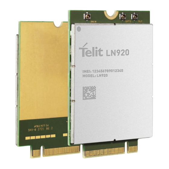
- Page 1 LN920 HW Design Guide Rev. 1 – 2021-08-11 1VV0301730 Telit Technical Documentation...
-
Page 2: Applicability Table
LN920 HW Design Guide APPLICABILITY TABLE PRODUCTS PART NUMBER LN920A12-WW LN920A12xxx LN920A6-WW LN920A6xxx 1VV0301730 Rev. 1 Page 2 of 81 2021-08-11 Not Subject to NDA... -
Page 3: Table Of Contents
Three Carrier Aggregation combinations (LN920A12-WW) 18 Mechanical Specifications 2.8.1. Dimensions 2.8.2. Weight Environmental Requirements 2.9.1. Temperature Range 2.9.2. RoHS Compliance PINS ALLOCATION Pin-out LN920 Signals for debugging purposes Pin Layout 1VV0301730 Rev. 1 Page 3 of 81 2021-08-11 Not Subject to NDA... - Page 4 LN920 HW Design Guide POWER SUPPLY Power Supply Requirements Power Consumption 4.2.1. Idle Mode 4.2.2. LN920 Connected Mode Current Consumption General Design Rules 4.3.1. Electrical Design Guidelines 4.3.1.1. +5V Source Power Supply Design Guidelines 4.3.2. Thermal Design Guidelines 4.3.3. Power Supply PCB Layout Guidelines...
- Page 5 GNSS Antenna Specifications 8.3.2. GNSS Antenna – Installation Guidelines GNSS Characteristics MECHANICAL DESIGN General Drawing APPLICATION GUIDE Debug of the LN920 Module in Production Bypass Capacitor on Power Supplies EMC Recommendations PACKAGING Tray CONFORMITY ASSESTMENT Approvals Summary RED Approval 12.2.1.
- Page 6 LN920 HW Design Guide 12.2.2. Antennas FCC et ISDE Approbation FCC and ISED Approval/ 12.3.1. FCC Certificate ISDE Approbation 12.3.2. ISED Approval/ Liste des Règles FCC et 12.3.3. Applicable FCC and ISED Rules / ISDE Applicables Avis Réglementaires de 12.3.4.
- Page 7 LN920 HW Design Guide GLOSSARY DOCUMENT HISTORY 1VV0301730 Rev. 1 Page 7 of 81 2021-08-11 Not Subject to NDA...
-
Page 8: Introduction
This document introduces the Telit LN920 module and presents possible and recommended hardware solutions for the development of a product based on this module. Features and solutions described in this document are applicable to all LN920 variants listed in the applicability table. - Page 9 LN920 HW Design Guide Our aim is to make this guide as helpful as possible. Keep us informed of your comments and suggestions for improvements. Telit appreciates the user feedback on our information. 1VV0301730 Rev. 1 Page 9 of 81...
-
Page 10: Symbol Conventions
Related Documents • LN920 SW User Guide, TBD • LN920 AT Commands Reference Guide, TBD • LN920 Interface Board HW User Guide, TBD • Generic EVB HW User Guide, 1VV0301249 1VV0301730 Rev. 1 Page 10 of 81 2021-08-11 Not Subject to NDA... -
Page 11: General Product Description
The aim of this document is to present possible and recommended hardware solutions useful for developing a product integrating Telit LN920 M.2 module. • LN920 is Telit’s M.2 form factor platform for applications, such as CPEs, routers and gateways, based on the following technologies:LN920A12-WW: LTE FDD/TDD Cat 12, up to 3CA DL (600 Mbps, 60 MHz) with WCDMA fallback •... -
Page 12: Configuration Pins
Configuration Pins Based on PCI Express M.2 Specification, LN920 has 4 configuration pins: they allow the host to identify the presence of an LN920 data card in the M.2 socket and identify main host interface and port configuration. The state of... - Page 13 Note: On the host side, each of the CONFIG_0 to CONFIG_4 pins require a pull-up resistor. Based on the configuration pins state on the LN920, being tied to GND or lifted to No Connect (NC), the sensed pins will create a 4-bit logic state.
-
Page 14: Block Diagram
LN920 HW Design Guide Block Diagram The diagram below shows an overview of the internal architecture of the LN920 data card. Figure 1: LN920 Block Diagram Transmit Output Power Band Power class 3G WCDMA Class 3 (0.2W) LTE All Bands (except B41) Class 3 (0.2W) - Page 15 LN920 HW Design Guide Technology 3GPP Compliance 4G LTE Throughput >95% 10MHz Dual Receiver 3G WCDMA BER <0.1% 12.2 Kbps Dual Receiver Table 7: Reception Sensitivity Product Band Sensitivity (dBm) LTE FDD B1 LTE FDD B2 LTE FDD B3 LTE FDD B4...
- Page 16 LN920 HW Design Guide Product Band Sensitivity (dBm) LTE FDD B25 LTE FDD B26 LTE FDD B28 LTE FDD B29 LTE FDD B30 LTE FDD B66 LTE FDD B71 LTE TDD B38 LTE TDD B39 LTE TDD B40 LTE TDD B41...
- Page 17 LN920 HW Design Guide REFsens (dBm) Band 3GPP REFsens (dBm)*/** Typical LTE Band26 -94.5 LTE Band28 -95.5 LTE Band29 LTE Band30 -96.0 LTE Band38 -97.0 LTE Band39 -97.0 LTE Band40 -97.0 LTE Band41 -95.0 LTE Band42 -96.0 LTE Band43 -96.0 LTE Band48 -96.0...
-
Page 18: Supported Carrier Aggregation Combinations
LN920 HW Design Guide Supported Carrier Aggregation combinations 2.7.1. Two Carrier Aggregation combinations (LN920A6-WW + LN920A12-WW) 2xCA Combinations (LN920A6-WW and LN920A12-WW) CA_1A-19A, CA_1A-1A, CA_1A-20A, CA_1A-26A, CA_1A-28A, CA_1A-38A, CA_1A-3A, CA_1A-40A, CA_1A-41A, CA_1A-42A, CA_1A-5A, CA_1A-7A, CA_1A-8A, CA_1C, CA_12A-12A, CA_12A-25A, CA_12A-30A, CA_12A-66A, CA_12B, CA_13A-66A, CA_14A-30A, CA_14A-66A, CA_18A-28A, CA_19A-42A, CA_2A-12A, CA_2A-13A, CA_2A-14A,... - Page 19 LN920 HW Design Guide 3xCA Combinations (LN920A12-WW) CA_4A-5A-30A, CA_4A-5B, CA_4A-7A-12A, CA_4A-7A-7A, CA_4A-7C, CA_40A-40C, CA_40A-42C, CA_40C-42A, CA_40D, CA_41A-41C, CA_41A-42C, CA_41C-42A, CA_41D, CA_42D, CA_48D, CA_5A-12B, CA_5A-29A-30A, CA_5A- 30A-66A, CA_5A-40A-40A, CA_5A-40C, CA_5A-5A-66A, CA_5A-66A-66A, CA_5A-66B, CA_5A-66C, CA_5A-7A-7A, CA_5A-7C, CA_5B-30A, CA_5B-66A, CA_66A-66A-71A, CA_66A-66B, CA_66A-66C, CA_66C-71A, CA_66D, CA_7B-...
-
Page 20: Mechanical Specifications
LN920 HW Design Guide Mechanical Specifications 2.8.1. Dimensions The overall dimensions of LN920A12-WW and LN920A6-WW modems are: • Length: 30.0 mm • Width: 42.0 mm • Thickness: Max. 2.3 mm 2.8.2. Weight The nominal weight of the LN920A12-WW is grams. -
Page 21: Rohs Compliance
LN920 HW Design Guide 2.9.2. RoHS Compliance As a part of the Telit corporate policy of environmental protection, the LN920 complies with the RoHS (Restriction of Hazardous Substances) directive of the European Union (EU directive 2011/65/EU). 1VV0301730 Rev. 1 Page 21 of 81... -
Page 22: Pins Allocation
LN920 HW Design Guide 3. PINS ALLOCATION Pin-out Signal Function Type Comment USB HS 2.0 COMMUNICATION PORT (FW upgrade and Data) USB_D+ USB differential Data (+) Analog USB_D- USB differential Data (-) Analog USB3.0_TX- USB 3.0 super-speed transmit - Minus Analog USB3.0_TX+... - Page 23 LN920 HW Design Guide Signal Function Type Comment 1.8V / WOW# Wake Host Open Drain 3.3V Dynamic Power Reduction 1.8V Active Low GPS_DISABLE# GPS disable 3.3V Internal PU COEX3 1.8V COEX_UART_RX 1.8V COEX_UART_TX 1.8V Active Low RESET# Reset Input 1.8V...
- Page 24 LN920 HW Design Guide Signal Function Type Comment VPH_PWR Power supply Power VPH_PWR Power supply Power VPH_PWR Power supply Power VPH_PWR Power supply Power VPH_PWR Power supply Power Ground Ground Ground Ground Ground Ground Ground Ground Ground Ground Ground Ground...
- Page 25 LN920 HW Design Guide Signal Function Type Comment No Connection Table Pin-out Information Warning: Unless otherwise specified, RESERVED pins must be left unconnected (Floating). 1VV0301730 Rev. 1 Page 25 of 81 2021-08-11 Not Subject to NDA...
-
Page 26: Ln920 Signals For Debugging Purposes
LN920 HW Design Guide LN920 Signals for debugging purposes The table below specifies the LN920 signals that must be connected for debugging purposes, even if not used by the end application. Mandatory Signals Signal Notes 2, 4, 70, 72, 74... -
Page 27: Pin Layout
LN920 HW Design Guide Pin Layout Figure 2: LN920 Pin-out 1VV0301730 Rev. 1 Page 27 of 81 2021-08-11 Not Subject to NDA... -
Page 28: Power Supply
The minimum voltage must be at least VBATT to power on the module. Power Consumption Below table provides typical current consumption values of LN920 for various operation modes. 1VV0301730 Rev. 1 Page 28 of 81 2021-08-11 Not Subject to NDA... -
Page 29: Idle Mode
Active State GPS+GLO, DPO on DWELL=280ms (GNSS ON, CFUN=5 eDRX) Navigation GPS+GLO, DPO off Table 16: GPS Mode *reference signal @-130 dbm with static scenario 4.2.2. LN920 Connected Mode Current Consumption Measure Mode Mode (Typical) Description Average Peak Connected mode... -
Page 30: General Design Rules
Mode Mode (Typical) Description WCDMA Table 17: LN920 Connected Mode Current consumption General Design Rules The main guidelines for the Power Supply Design include three different design steps: • Electrical design of the power supply • Thermal design • PCB layout 4.3.1. -
Page 31: Thermal Design Guidelines
Module, a 100μF capacitor is usually suitable. • Make sure the low ESR capacitor on the power supply output rated at least 10V. • A protection diode must be inserted close to the power input to protect the LN920 module from power polarity inversion. 4.3.2. -
Page 32: Power Supply Pcb Layout Guidelines
TBD A current peak is absorbed. • The PCB traces to the LN920 and the Bypass capacitor must be wide enough to ensure no significant voltage drops occurs. This is for the same reason as previous point. -
Page 33: Rtc (Real Time Clock)
RTC (Real Time Clock) The RTC function is provided to keep time information with low power consumption even when the LN920 is turned off. It is also provided to enable alarm wake-up when the LN920 is turned off. 1VV0301730 Rev. 1... -
Page 34: Electrical Specifications
LN920 HW Design Guide 5. ELECTRICAL SPECIFICATIONS Absolute Maximum Ratings – Not Optional Warning: A deviation from the value ranges listed below may harm the LN920 module. Parameter Parameter Unit VBATT Battery supply voltage on pin VBATT -0.5 +4.2 Recommended Operating Conditions... -
Page 35: Digital Section
• OFF state: Vbatt is applied and only RTC is running. Baseband is switched OFF and the only transition possible is the ON state. • ON state: Baseband is fully switched on and LN920 is ready to respond to AT commands. The modem can be idle or connected. -
Page 36: Logic Levels
LN920 HW Design Guide Logic Levels Parameter ABSOLUTE MAXIMUM RATINGS – NOT FUNCTIONAL Input level on any digital pin (CMOS 1.8) with respect to ground Operating Range - Interface levels (1.8V CMOS) Input high level Input low level Output high level... -
Page 37: Power On
6.2.1. Initialization and Activation State After turning on the LN920, the module is not instantly activated because the SW initialization For this reason, it is recommended not to process takes some time to complete. communicate with the LN920 during this initialization phase. -
Page 38: Power Off
LN920 HW Design Guide Boot OK (Shutdown indicator) is an optional function and is disabled by default. Host can use the AT#SHDNIND command to assign one of the GPIOs as the Boot OK pin. After enabling the function, the corresponding pin operates as a Book OK and also Shutdown Indicator function. -
Page 39: Graceful Shutdown
LN920 HW Design Guide 6.3.1. Graceful Shutdown To safely power off the LN920 module, the host can use the graceful shutdown function. To gracefully shutdown the LN920 module, FULL_CARD_POEWR_OFF# should be asserted Low. Once FULL_CARD_POWER_OFF# is asserted LOW, the LN920 module enters finalization state, terminates active processes and prepare to turn off safely. - Page 40 LN920 HW Design Guide When the status transitions to Low, the module is ready to shutdown. Shutdown Indicator (Boot OK) is optional function and is disabled by default. Host can use the AT#SHDNIND command to assign one of the GPIOs as the Shutdown Indicator pin.
-
Page 41: Reset
Device reset can be triggered by Unconditional reset using the RESET#. 6.4.1. Unconditional Hardware Reset To unconditionally restart the LN920 module, the RESET# pin must be asserted LOW for more than 1 second, then released. As shown in the diagram below,... -
Page 42: Communication Ports
Revision 3.0 and can be used for control and data transfers as well as for diagnostic monitoring and firmware update. The USB port is the main interface between the LN920 module and the host controlling the modem hardware. 1VV0301730 Rev. 1... - Page 43 USB 3.0 needs AC coupling series capacitors on the TX lines in both directions. In order to interface USB3.0 with the application board controlling the modem, 0.1uF capacitors should be installed on USB_SS_RX_P/M lines of the LN920. Series capacitors are already placed on USB_SS_TX_P/M lines inside LN920 module.
-
Page 44: Sim Interface
LN920 HW Design Guide 6.5.2. SIM Interface The LN920 supports two external SIM interfaces (1.8V or 2.85V). Signal Function Type SIM Card Interface 1 Supply output for UIM1_PWR 1.8V / 2.85V external UIM1 card Data connection UIM1_DATA with an 1.85 / 2.85V... -
Page 45: Sim Schematic Example
6.5.2.1. SIM Schematic Example The following diagrams illustrate how the application interface should be designed. Note: LN920 contains an internal pull-up resistor on SIMIO lines, thus it is not necessary to install external pull-up resistors. 6.5.3. Control Signals The LN920 supports the following control signals: •... -
Page 46: General Purpose I/O
LN920 HW Design Guide Internal VBATT GPS_DISABLE# GPS disable pull-up Wake the WOW# plaform by the Open-drain WWAN device WWAN_LED# LED control Open-drain WWAN_LED# signal drives the LED output to display network registration state. The recommended LED connection is the following: R1 and VDD determine the brightness of LED and forward current. -
Page 47: Using A Gpio As Input
1.8V CMOS levels of the GPIO. If the digital output of the device to be connected with the GPIO input pin of LN920 has interface levels different from the 1.8V CMOS, then it can be buffered with an open collector transistor with a 47K pull up to 1.8V. -
Page 48: I2C - Inter-Integrated Circuit
LN920 HW Design Guide GPIO Output Pin Equivalent Circuit I2C – Inter-integrated circuit The LN920 supports an I2C interface on the following pins: Signal Function Type NOTE I2C_SDA I2C Data CMOS 1.8V I2C_SCL I2C Clock CMOS 1.8V The I2C interface is used for controlling peripherals from within the module (such as sensors, codecs, etc.) -
Page 49: Rf Section
LN920 HW Design Guide 7. RF SECTION Bands Variants Product Bands B1, B2, B3, B4, B5, B7, B8, B12, B13, B14, B17, B18, B19, B20, B25, B26, B28, LN920A12-WW B29, B30, B38, B39, B40, B41, B42, B43, B48, B66, B71... -
Page 50: Antenna Requirements
Hence, please read carefully and follow the requirements and the guidelines for a proper design. The antenna and RF transmission line on host PCB for a Telit LN920 based device shall fulfil the following requirements: 1VV0301730 Rev. -
Page 51: Antenna Configration
Table 26: LN920 Antenna and Antenna Transmission Line on PCB 7.4.1. Antenna Configration LN920 modems provide two MHF-4 type RF connectors for LTE/WCDMA and GNSS bands and one MHF-4 type RF connector dedicated to the GNSS receiver. The diagram below shows the connectors position on the modem board. - Page 52 LN920 HW Design Guide Figure 3: Antenna Configration Refer to the following antenna configuration assigned. Antenna port Technology GNSS WCDMA B1, B2, B4, B5, B8, B9, B19 B1, B2, B4, B5, B8, B9, B19 B1, B2, B3, B4, B5, B7, B8,...
-
Page 53: Antenna Connector
LN920 HW Design Guide 7.4.2. Antenna Connector The LN920 Family is equipped with a set of 50 Ω RF MHF-4 Receptacle from I-PEX 20449- 001E https://www.i-pex.com For more information about mating connectors, please consult: Figure 4: MHF-4 RF connector 1VV0301730 Rev. 1... -
Page 54: Antenna Cable
LN920 HW Design Guide Figure 5: MHF-4 Receptacle If FCC certification is required for an application using LN920, according to FCC KDB 996369 for modular approval requirements, the transmission line must be similar to the one implemented on the LN920 interface board and described in the following chapter. - Page 55 LN920 HW Design Guide • In order to meet the related EIRP limitations, antenna gain must not exceed the values indicated in regulatory requirements, where applicable. The Typical antenna Gain in most M2M applications does not exceed 2dBi. • If the device antenna is located farther than 20 cm from the human body and there are no co-located transmitters, then the Telit FCC/IC approvals can be re-used by the end product.
-
Page 56: Gnss Section
LN920 HW Design Guide 8. GNSS SECTION The LN920 module includes a state-of-art receiver that can simultaneously search and track satellite signals from multiple satellite constellations. This multi-GNSS receiver uses the entire spectrum of GNSS systems available: GPS, GLONASS, BeiDou, Galileo. -
Page 57: Hardware-Based Solution For Gnss And Lte Coexistence
GNSS antennas is low. A SAW filter can be added on LTE side to protect the GNSS receiver from LTE out-of-band emissions, as described in the schematic below. When the GNSS receiver embedded in the LN920 module is used, the LTE transmitter and the GNSS receiver are never simultaneously active, thus filtering on the LTE side is not needed. -
Page 58: Gnss Antenna Requirements
LN920 HW Design Guide GNSS Antenna Requirements For most applications, it is recommented to use an active GNSS antenna. 8.3.1. GNSS Antenna Specifications Item Value Frequency range 1559.0 ~ 1610.0 MHz Gain 15 ~ 30dB Impedance 50 ohm Noise Figure of LNA <... - Page 59 LN920 HW Design Guide Min Navigation update rate Table 30: GNSS Characteristics 1VV0301730 Rev. 1 Page 59 of 81 2021-08-11 Not Subject to NDA...
-
Page 60: Mechanical Design
LN920 HW Design Guide 9. MECHANICAL DESIGN General The LN920 module was designed to be compliant with a standard lead-free SMT process. Drawing Figure 7: Mechanical Design Drawing 1VV0301730 Rev. 1 Page 60 of 81 2021-08-11 Not Subject to NDA... -
Page 61: Application Guide
10. APPLICATION GUIDE Debug of the LN920 Module in Production To test and debug the LN920 module integration, it is strongly recommended to add test points on the host PCB for the following purposes: • Checking the connection between the LN920 itself and the application •... -
Page 62: Emc Recommendations
And if fast power down function is used, additional bypass capacitors should be mounted on the application board. EMC Recommendations EMC protection on all the pins of LN920 should be designed by application side according to the customer’s requirement. ESD rating on all pins of LN920 Family : Human Body Model (HBM): ±... -
Page 63: Packaging
LN920 HW Design Guide 11. PACKAGING Tray The LN920 module is packaged on trays of pieces each. These trays can be used in SMT processes for pick & place handling. Figure 8: Tray Packaging 1VV0301730 Rev. 1 Page 63 of 81... - Page 64 LN920 HW Design Guide Figure 9: Tray Dimensions 1VV0301730 Rev. 1 Page 64 of 81 2021-08-11 Not Subject to NDA...
-
Page 65: Conformity Assestment
LN920 HW Design Guide 12. CONFORMITY ASSESTMENT Approvals Summary Module ISED ANATEL JRF&JTBL LN920A12-WW LN920A6-WW ApprovalsTable 31: Approvals Summary RED Approval 12.2.1. RED Declaration of Conformity Hereby, Telit Communications S.p.A declares that the XX123Z4-W1, XX123Z4-WW and XX123Z4-WWV Modules are in compliance with Directive 2014/53/EU. -
Page 66: Fcc And Ised Approval/Fcc Et Isde Approbation
LN920 HW Design Guide Max Gain for RED (dBi) FDD 20 FDD 28 Table 33: Max Gain for RED FCC et ISDE Approbation FCC and ISED Approval/ 12.3.1. FCC Certificate The FCC Certifcate is available here: https://www.fcc.gov/oet/ea/fccid ISDE Approbation 12.3.2. - Page 67 LN920 HW Design Guide Déclaration d'interférence Interference statement / This device complies with Part 15 of the FCC Rules and Industry Canada licence-exempt RSS standard(s). Operation is subject to the following two conditions: (1) this device may not cause interference, and (2) this device must accept any interference, including interference that may cause undesired operation of the device.
-
Page 68: Antennas / Antennes
LN920 HW Design Guide • Increase the separation between the equipment and receiver. • Connect the equipment into an outlet on a circuit different from that to which the receiver is connected. • Consult the dealer or an experienced radio/TV technician for help. - Page 69 LN920 HW Design Guide Max Gain for FCC (dBi) Table 36: Max Gain for FCC (dBi) ISED / ISDE This radio transmitter has been approved by ISED to operate with the antenna types listed below with the maximum permissible gain indicated. Antenna types not included in this list, having a gain greater than the maximum gain indicated for that type, are strictly prohibited for use with this device.
-
Page 70: Fcc Label And Compliance Information
LN920 HW Design Guide Gain maximum pour ISDE (dBi) Gain maximum pour ISED (dBi) / Table 38: Gain Maximum for ISED (dBi) 12.3.6. FCC Label and Compliance Information The product has a FCC ID label on the device itself. Also, the OEM host end product manufacturer will be informed to display a label referring to the enclosed module The exterior label will read as follows: “Contains Transmitter Module FCC ID: RI7... -
Page 71: Information On Test Modes And Additional Testing Requirements / Informations Sur Les Modes De Test Et Les Exigences De Test Supplémentaires
LN920 HW Design Guide In this case, XXXXXX-YYYYYYYYYYY is the module's certification number. Le produit hôte devra être correctement étiqueté, de façon à permettre l'identification des modules qui s'y trouvent. L'étiquette d'homologation d'un module d'ISDE devra être apposée sur le produit hôte à... -
Page 72: Fcc Additional Testing, Part 15 Subpart B Disclaimer
LN920 HW Design Guide 12.3.9. Fcc Additional Testing, Part 15 Subpart B Disclaimer The modular transmitter is only FCC authorized for the specific rule parts (i.e., FCC transmitter rules) listed on the grant, and that the host product manufacturer is responsible for compliance to any other FCC rules that apply to the host not covered by the modular transmitter grant of certification. -
Page 73: Reference Table Of Rf Bands Characteristics
LN920 HW Design Guide 13. REFERENCE TABLE OF RF BANDS CHARACTERISTICS Mode Freq. Tx (MHz) Freq. Rx (MHz) Channels Tx-Rx Offset PCS 1900 1850.2 ~ 1909.8 1930.2 ~ 1989.8 512 ~ 810 80 MHz DCS 1800 1710 ~ 1785 1805 ~ 1880... - Page 74 LN920 HW Design Guide Mode Freq. Tx (MHz) Freq. Rx (MHz) Channels Tx-Rx Offset Tx: 21450 ~ 21799 LTE 900 – B8 880 ~ 915 925 ~ 960 45 MHz Rx: 3450 ~ 3799 Tx: 21800 ~ 2149 LTE 1800 – B9 1749.9 ~ 1784.9...
-
Page 75: Product And Safety Information
LN920 HW Design Guide 14. PRODUCT AND SAFETY INFORMATION Copyrights and Other Notices SPECIFICATIONS ARE SUBJECT TO CHANGE WITHOUT NOTICE Although reasonable efforts have been made to ensure the accuracy of this document, Telit assumes no liability resulting from any inaccuracies or omissions in this document, or from the use of the information contained herein. -
Page 76: Usage And Disclosure Restrictions
LN920 HW Design Guide computer programs, including – but not limited to - the exclusive right to copy or reproduce in any form the copyrighted products. Accordingly, any copyrighted computer programs contained in Telit’s products described in this instruction manual shall not be copied (reverse engineered) or reproduced in any manner without the express written permission of the copyright owner, being Telit or the Third Party software supplier. -
Page 77: Trademarks
LN920 HW Design Guide 14.2.4. Trademarks TELIT and the Stylized T-Logo are registered in the Trademark Office. All other product or service names are property of their respective owners. 14.2.5. 3rd Party Rights The software may include Third Party’s software Rights. In this case the user agrees to comply with all terms and conditions imposed in respect of such separate software rights. -
Page 78: Safety Recommendations
LN920 HW Design Guide Safety Recommendations Make sure the use of this product is allowed in your country and in the environment required. The use of this product may be dangerous and has to be avoided in areas where: • it can interfere with other electronic devices, particularly in environments such as hospitals, airports, aircrafts, etc. - Page 79 LN920 HW Design Guide 15. GLOSSARY Analog – Digital Converter Clock CMOS Complementary Metal – Oxide Semiconductor Chip Select Digital – Analog Converter Data Terminal Equipment Equivalent Series Resistance GPIO General Purpose Input Output High Speed HSDPA High Speed Downlink Packet Access...
- Page 80 LN920 HW Design Guide 16. DOCUMENT HISTORY Revision Date Changes 2021-06-30 First Draft 2021-08-11 Carrier Aggregation (CA) combinations tables added From Mod.0818 rev.2 1VV0301730 Rev. 1 Page 80 of 81 2021-08-11 Not Subject to NDA...
Need help?
Do you have a question about the LN920 and is the answer not in the manual?
Questions and answers