Telit Wireless Solutions ME310G1 Hw Design Manual
Hide thumbs
Also See for ME310G1:
- Reference manual (1039 pages) ,
- At commands reference manual (545 pages) ,
- Hw design manual (88 pages)

Related Manuals for Telit Wireless Solutions ME310G1


Summary of Contents for Telit Wireless Solutions ME310G1
- Page 1 ME310G1 HW Design Guide 1VV0301588 Rev. 16 – 2021-10-27 Telit Technical Documentation...
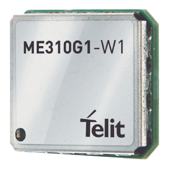
- Page 2 ME310G1 Hardware Design Guide APPLICABILITY TABLE PRODUCTS ME310G1-W1 ME310G1-WW ME310G1-WWV ME310G1-W2 ME310G1-W3 1VV0301588 Rev. 16 Page 2 of 95 2021-10-27 Not Subject to NDA...
-
Page 3: Table Of Contents
ME310G1 Hardware Design Guide CONTENTS Scope Audience Contact Information, Support Symbol Conventions Related Documents Overview Product Variants and Frequency Bands Target Market Main Features TX Output Power 2.5.1 ME310G1-W1 2.5.2 ME310G1-WW 2.5.3 ME310G1-WWV 2.5.4 ME310G1-W2 2.5.5 ME310G1-W3 RX Sensitivity 2.6.1 ME310G1-W1 2.6.2... - Page 4 ME310G1 Hardware Design Guide LGA Pads Layout Power Supply Requirements Power Consumption 4.2.1 Idle Mode 4.2.2 ME310G1-W1 Connected Mode 4.2.3 ME310G1-WW and ME310G1-WWV Connected Mode 4.2.4 ME310G1-W2 Connected Mode 4.2.5 ME310G1-W3 Connected Mode General Design Rules 4.3.1 Electrical Design Guidelines 4.3.1.1 +5V Source Power Supply Design Guidelines 4.3.1.2...
- Page 5 ME310G1 Hardware Design Guide 5.7.3.1 Asynchronous Serial Port (USIF1) 5.7.3.2 Auxiliary Serial Port General Purpose I/O 5.8.1 Using a GPIO as INPUT 5.8.2 Using a GPIO as OUTPUT External SIM Holder 5.10 ADC Converter 5.10.1 Using ADC Converter 5.11 DAC Converter 5.11.1...
- Page 6 ME310G1 Hardware Design Guide 8.3.2 GNSS Antenna – Installation Guidelines 8.3.3 Powering the External LNA (Active Antenna) GNSS Characteristics Drawing 9.1.1 ME310G1-W1 9.1.2 ME310G1-WW, ME310G1-WWV, ME310G1-W2, and ME310G1- 10.1 Footprint 10.1.1 ME310G1-W1 10.1.2 ME310G1-WW, ME310G1-WWV, ME310G1-W2, and ME310G1- 10.1.3 Recommendations for ME310G1-W1 10.1.4...
- Page 7 ME310G1 Hardware Design Guide 12.2.2 UKCA Declaration of Conformity 12.2.3 RED/UKCA Antennas FCC et ISDE Approbation 12.3 FCC and ISED Approval/ 12.3.1 FCC Certificates ISDE Certificates 12.3.2 ISED Certificate / Liste des Règles FCC et 12.3.3 Applicable FCC and ISED Rules / ISDE Applicables Avis Réglementaires de...
- Page 8 ME310G1 Hardware Design Guide 1VV0301588 Rev. 16 Page 8 of 95 2021-10-27 Not Subject to NDA...
-
Page 9: Scope
Telit ME310G1 module well and quickly develop various products. Audience This document is intended for system integrators who use the Telit ME310G1 module in their products. Contact Information, Support... -
Page 10: Symbol Conventions
ME310G1 Hardware Design Guide Symbol Conventions Danger: This information MUST be followed, or catastrophic equipment failure or personal injury may occur. Warning: Alerts the user on important steps about the module integration. Note/Tip: Provides advice and suggestions that may be useful when integrating the module. -
Page 11: Overview
The Telit ME310G1 module is a CATM / NBIoT communication module that allows integrators to plan availability for lifecycle applications. The Telit ME310G1-WWV module is fully voice capable with a Digital Voice Interface (DVI). It is suitable for applications such as voice-enabled alarm panels, mHealth patient monitors, and special devices used by elderly or disabled. -
Page 12: Target Market
B8_39d. that is AT#BNDOPTIONS? #BNDOPTIONS: 1,2,3,4,5,8,12,13,18,19,20,25,26,27,28,66,71,85, B8_39d. Target Market The Telit ME310G1 can be used for telematics applications where tamper-resistance, confidentiality, integrity, and authenticity of end-user information are required, for example: • Telematics services • Road pricing •... -
Page 13: Main Features
B1, B2, B3, B4, B5, B8, B12, B13, B18, B19, (LTE) CAT-NB2 B20, B25, B26, B28, B66, B85, B86, B8_39d (LTE) CAT-NB2 Table 5: Transmission Output Power ME310G1-WW 1VV0301588 Rev. 16 Page 13 of 95 2021-10-27 Not Subject to NDA... -
Page 14: Me310G1-Wwv
B19, B20, B25, B26, B27, B28, B66, B85 B1, B2, B3, B4, B5, B8, B12, B13, B18, (LTE) CAT-NB2 B19, B20, B25, B26, B28, B66, B85 (LTE) CAT-NB2 Table 6: Transmission Output Power ME310G1-WWV 2.5.4 ME310G1-W2 RF power (dBm) Band... -
Page 15: Rx Sensitivity
ME310G1 Hardware Design Guide RX Sensitivity 2.6.1 ME310G1-W1 REFsens (dBm) REFsens (dBm)* Band Typical 3GPP Limit CATM1 / Band1 -107.1 -102.7 CAT M1 / Band2 -107.5 -100.3 CAT M1 / Band3 -106.4 -99.3 CAT M1 / Band4 -107.3 -102.3 CAT M1 / Band5 -106.0... -
Page 16: Me310G1-Ww
-108.2 CAT NB2 / Band66 -115.3 -108.2 CAT NB2 / Band71 -111.3 CAT NB2 / Band85 -115.7 Table 9: RX Sensitivity ME310G1-W1 * 3GPP TS 36.521-1 release 15 minimum performance requirement 2.6.2 ME310G1-WW REFsens (dBm) REFsens (dBm)* Band Typical 3GPP Limit CATM1 / Band1 -105.6... - Page 17 -108.2 CAT NB2 / Band66 -115.2 -108.2 CAT NB2 / Band71 -107.5 CAT NB2 / Band85 -115.5 Table 10: RX Sensitivity ME310G1-WW * 3GPP TS 36.521-1 release 15 minimum performance requirement 2.6.3 ME310G1-W2 REFsens (dBm) REFsens (dBm)* Band Typical 3GPP Limit CATM1 / Band1 -106.6...
-
Page 18: Me310G1-W3
• Width: 15.0 mm • Thickness: 2.6 mm 2.7.2 Weight The nominal weight of the ME310G1-W1 is 1 Gram. The nominal weight of the ME310G1-WW, ME310G1-WWV, and ME310G1-W2 is 1.5 Gram. 1VV0301588 Rev. 16 Page 18 of 95 2021-10-27 Not Subject to NDA... -
Page 19: Temperature Range
ME310G1 Hardware Design Guide Temperature Range Temperature range Note The module is fully functional (*) and compliant Operating Temperature Range –40°C to +85°C according to regulatory standards. The module is not powered and not connected Storage Temperature Range –40°C to +105°C... -
Page 20: Pin-Out
ME310G1 Hardware Design Guide 3 PINS ALLOCATION Pin-out Signal Function Type Comment USB HS 2.0 Communication Port USB_D+ USB differential Data (+) USB_D- USB differential Data (-) USB_VBUS USB Power Sense Asynchronous Serial Port (USIF0) – Prog. / Data + HW Flow Control... - Page 21 ME310G1 Hardware Design Guide Signal Function Type Comment Only 1.8V simcard SIM_VCC Power supply for the SIM 1.8V are supported SIMIN Presence SIM input CMOS 1.8V See par.5.8 SPI_MOSI SPI MOSI CMOS 1.8V SPI_MISO SPI MISO CMOS 1.8V SPI_CLK SPI Clock CMOS 1.8V...
- Page 22 ME310G1 Hardware Design Guide Signal Function Type Comment Input Command for Power ON_OFF*/WAKE* ON/OFF and to wake from deep CMOS 1.8V Active Low sleep mode PWRMON Power ON Monitor CMOS 1.8V Active high, Optional pin, connect to test FORCED_USB_BOOT CMOS 1.8V...
- Page 23 ME310G1 Hardware Design Guide Signal Function Type Comment RF Ground Power Thermal Ground Power Thermal Ground Power Thermal Ground Power Thermal Ground Power Thermal Ground Power Thermal Ground Power Thermal Ground Power Thermal Ground Power Thermal Ground Power Thermal Ground...
- Page 24 ME310G1 Hardware Design Guide Signal Function Type Comment RESERVED RESERVED RESERVED RESERVED RESERVED RESERVED RESERVED RESERVED RESERVED RESERVED RESERVED RESERVED RESERVED RESERVED RESERVED RESERVED Table 14: Pin-out Information Warning: Reserved pins must not be connected. All pull-up (PU) and pull-down (PD) are about 100K.
-
Page 25: Lga Pads Layout
ME310G1 Hardware Design Guide LGA Pads Layout TOP VIEW (HW 1.0) CELL MAIN S_LED DVI_W DVI_R DVI_T GNSS DVI_C ATC1 GNSS_ MIPI_C 1PPS GNSS_ LNA_E ATC2 MIPI_D SIM_C SIM_R ON_OF SIM_D CTANK F*/WA SIM_V PWRM FORCE USB_V D_USB_ BOOT USB_D... -
Page 26: Power Supply Requirements
ME310G1 Hardware Design Guide 4 POWER SUPPLY The power supply circuit and board layout are an important part of the product design. Make sure to follow the guidelines and requirements for optimal performance. Power Supply Requirements The external power supply must be connected to the VBATT & VBATT_PA signals. The... -
Page 27: Power Consumption
ME310G1 Hardware Design Guide Note: The Hardware User Guide specifications must be recognized and carefully implemented to use the module in its Extended Operating Voltage Range. Power Consumption 4.2.1 Idle Mode Measure Mode Mode (Typical) Description CATM NBIoT IDLE mode... -
Page 28: Me310G1-W1 Connected Mode
3.75KHz subcarrier spacing, 1 SC, RU 32ms, TBS=0, BPSK, 21dBm, all bands NBIoT 15KHz subcarrier spacing, 12 SC, RU 1ms, TBS=5, QPSK, 21dBm, all bands Table 18: ME310G1-W1 connected mode 4.2.3 ME310G1-WW and ME310G1-WWV Connected Mode Measure Mode (Typical) -
Page 29: Me310G1-W2 Connected Mode
23dBm, Band 3, 2, 25, 4, 1, 66 2000 1TX + 1RX, CS1, GMSK, Band 850, 900 GPRS 1000 1TX + 1RX, CS1, GMSK, Band 1800, 1900 Table 19: ME310G1-WW and ME310G1-WWV Connected Mode 4.2.4 ME310G1-W2 Connected Mode Measure Mode Mode... -
Page 30: Me310G1-W3 Connected Mode
1 RB, RMC, TBS=5, QPSK,23dBm, Band 26, 5 CATM 1 RB, RMC, TBS=5, QPSK, 23dBm, Band 3 Table 21: ME310G1-W3 Connected Mode General Design Rules The Power Supply Design guidelines include three different design steps: • Electrical design • Thermal design •... -
Page 31: Source Power Supply Design Guidelines
ME310G1 Hardware Design Guide An example of a linear regulator with 5V input is: Figure 3: Example of a linear regulator with 5V input 4.3.1.2 +12V Source Power Supply Design Guidelines The desired output for the power supply is 3.8V, so due to the large difference between the input source and the desired output, a linear regulator is not suitable and shall not be used. -
Page 32: Battery Source Power Supply Design Guidelines
The nominal output of the desired power supply is 3.8V and the maximum voltage is 4.2V. So a single 3.7V Li-Ion battery type is sufficient to power the Telit ME310G1 module. • A low ESR bypass capacitor must be included to stop the current absorption peaks near the module. -
Page 33: Power Supply Pcb Layout Guidelines
A misplaced component can be useless or can even decrease the power supply performance. • The low ESR Bypass capacitor must be placed near the Telit ME310G1 power input pads or, if the power supply is of the switching type, it can be placed near... -
Page 34: Rtc Supply
The below figure shows the recommended circuit: Figure 5: Recommended circuit RTC Supply RTC is functional when ME310G1 is in PSM or OFF state and VBATT pin is supplied. RTC settings are lost when the VBATT supply is disconnected. PWRMON Power-on Monitor PWRMON is always active (output high) when the module is powered ON (module powered ON indication) and cannot be set to a LOW level with AT commands. - Page 35 ME310G1 Hardware Design Guide Note: PWRMON during the PSM period is LOW. (PSM must be previously enabled by AT+CPSMS command). Warning: This signal is NOT provided to supply small devices from the module. PWRMON is only a module power-on indicator.
-
Page 36: Logic Levels
ME310G1 Hardware Design Guide 5 DIGITAL SECTION ME310G1 has four main operation states: • OFF state: VBATT is applied and only RTC is running. The Baseband is switched OFF and the only possible change is the ON state. • ON state: The baseband is fully switched on and the module is ready to accept AT commands. -
Page 37: Power On
ME310G1 Hardware Design Guide Power On The following flow chart shows the proper “Modem Turn ON” procedure. Figure 6: Modem On Process flow chart In some use cases ON_OFF* can be tied fix LOW considering two limitations: 1. PSM wake-up asynchronous capability will be lost. -
Page 38: Power Off
ME310G1 Hardware Design Guide Power Off The proper procedure to power off the module is to use the AT#SHDN command. An alternative procedure is to use the ON_OFF* pin as described in the following procedure: Figure 7: Modem OFF Process flow chart 1VV0301588 Rev. -
Page 39: Unconditional Shutdown
The following flow chart shows the proper procedure for an unconditional shutdown of the Telit ME310G1 module, except in PSM mode. When the procedure is completed the module is reset and stops all operations. After the release of the line, the module is unconditionally shut down, without performing any disconnection from the network in which it is registered. -
Page 40: Wake Up From Deep Sleep Mode
The host can detect deep sleep mode by pulling the PWRMON pin if PSM has been previously configured. Fast Shut Down The procedure to power off the Telit ME310G1 module is explained in the Power Off section. It normally takes more than a second to disconnect from the network and properly close the internal filesystem. -
Page 41: Fast Shut Down By Software
The Fast Shut Down can be triggered by AT command. Communication Ports 5.7.1 USB 2.0 HS The Telit ME310G1 module includes an integrated universal serial bus (USB 2.0 HS) transceiver. The following table lists the available signals: Signal Function NOTE... -
Page 42: Spi
ME310G1 Hardware Design Guide 5.7.2 The Telit ME310G1 module is provided by a standard 3-wire SPI master or slave interface with chip select control. The following are the available signals: Signal Function Type NOTE SPI_MOSI SPI MOSI CMOS 1.8V SPI_MISO SPI MISO CMOS 1.8V... -
Page 43: Asynchronous Serial Port (Usif0)
ME310G1 Hardware Design Guide 5.7.3.1.Asynchronous Serial Port (USIF0) The serial port 0 on the Telit ME310G1 module is a +1.8V UART with 5 RS232 signals. It differs from the PC-RS232 in signal polarity (RS232 is reversed) and levels. The following are the available signals:... -
Page 44: Asynchronous Serial Port (Usif1)
5.7.3.1 Asynchronous Serial Port (USIF1) The serial port 1 on the Telit ME310G1 module is a +1.8V UART with 5 RS232 signals. It differs from PC-RS232 in signal polarity (RS232 is reversed) and levels. Warning: C104/RXD1 cannot have any PU or HIGH state during BOOTING UP phase. -
Page 45: General Purpose I/O
Table 31: ME310G1 serial port signals General Purpose I/O The Telit ME310G1 module includes a set of configurable digital input and output pins (CMOS 1.8V). The Input pads can only be read. They report the digital value (high or low) present on the pad at the time of reading. -
Page 46: Using A Gpio As Output
5.10 ADC Converter The Telit ME310G1 module includes an AD converter. It can read a voltage level in the range of 0÷1.8V applied on the ADC pin input, store it and convert it to 10-bit words. -
Page 47: Using Adc Converter
5.10.1 Using ADC Converter Available in the next document revision. 5.11 DAC Converter The Telit ME310G1 module includes a Digital Analog Converter. The signal (named DAC) is available on pin R16 of the module. 5.11.1 Enabling DAC Available in a next document revision. -
Page 48: Antenna Tuner
ME310G1 Hardware Design Guide 5.14 Antenna Tuner The Telit ME310G1 module includes a feature to enable an external antenna tuning solution. This enables to dynamically tune the antenna on multiple frequencies. Refer to AT command AT#ATUNERSEL (AT Commands Reference Guide-Telit code 80617ST10991A) to select GPIO or MIPI interfaces on ATC1/ATC2 pins. -
Page 49: Antenna Requirements
VSWR absolute max ≤ 10:1 (limit to avoid permanent damage) VSWR recommended ≤ 2:1 (limit to fulfill all regulatory requirements) Table 35: ME310G1 Antenna and Antenna transmission line on PCB 1VV0301588 Rev. 16 Page 49 of 95 2021-10-27 Not Subject to NDA... -
Page 50: Pcb Design Guidelines
ME310G1 Hardware Design Guide 6.1.1 PCB Design Guidelines As there is no antenna connector on the ME310G1 module, you must use a transmission line to connect the antenna to the antenna pad on the PCB. The following are the transmission line requirements:... -
Page 51: Pcb Guidelines In Case Of Fcc Certification
ME310G1 Hardware Design Guide • Place the noisy EM devices as far as possible away from the ME310G1 antenna line. • Keep the antenna line far away from the ME310G1 power supply lines. • If there are noisy EM devices (such as fast switching ICs, LCD, and so on) on... -
Page 52: Transmission Line Design
ME310G1 Hardware Design Guide 6.1.2.1 Transmission Line Design When designing the ME310G1 interface board, the placement of components was chosen properly, in order to keep the line length as short as possible, thus leading to the lowest possible power losses. A Grounded Coplanar Waveguide (G-CPW) line was chosen, since this kind of transmission line ensures good impedance control and can be implemented in an outer PCB layer as needed in this case. - Page 53 ME310G1 Hardware Design Guide transmission line including the connector itself. During Return Loss / impedance measurements, the transmission line has been terminated to 50 Ω load. Return Loss plot of line under test is shown below: Figure 13: Return Loss plot of line under test Line input impedance (in Smith Chart format, once the line has been terminated to 50 Ω...
-
Page 54: Antenna Installation Guidelines
ME310G1 Hardware Design Guide Figure 15: Insertion Loss of G-CPW line plus SMA connector 6.1.2.3 Antenna Installation Guidelines • Install the antenna in a place covered by the LTE signal with CAT-M1 support. • The Antenna must not be installed inside metal cases. - Page 55 ME310G1 Hardware Design Guide • If the device antenna is located closer than 20cm from the human body or there are co-located transmitter , the additional FCC/IC testing may be required for the end product (Telit FCC/IC approvals cannot be reused).
-
Page 56: Electrical Characteristics
ME310G1 Hardware Design Guide 7 AUDIO SECTION The Telit ME310G1 Module’s digital voice interface is based on the I2S serial bus interface. The audio port can be connected to the digital interface which uses multiple compliant codecs (in case analog audio is needed). The audio port is available only in ME310G1-WWV that has CS Voice/VoLTE support. -
Page 57: Gnss Signals Pin-Out
SW releases. RF Front End Design The ME310G1 module does not contain the LNA required to achieve maximum sensitivity. The active antenna (antenna with a built-in low noise amplifier) must be supplied with a proper bias-tee circuit. -
Page 58: Hardware-Based Solution For Gnss And Lte Coexistence
LTE out-of-band emissions, include a SAW filter on the LTE side as described in the diagram below. There is no condition to degrade the GNSS receiver embedded in the ME310G1 module while it is in use. So filtering on the LTE is not mandatory as the LTE and GNSS cannot be active at the same time. -
Page 59: Gnss Antenna Specification
Powering the External LNA (Active Antenna) The active antenna requires either 1.8V or 3V DC power supply. To meet this requirement, an external power source with the ME310G1 module must be included in the user’s application circuit. The electrical characteristics of the GPS_LNA_EN signal are:... -
Page 60: Gnss Characteristics
ME310G1 Hardware Design Guide Example of external antenna bias circuitry: Figure 17: Antenna bias circuitry example Warning: Ensure to regulate the maximum bias current. A short circuit on the antenna cable may damage the decoupling inductor. GNSS Characteristics The following table specifies the GNSS characteristics and the expected performance. -
Page 61: Drawing
ME310G1 Hardware Design Guide 9 MECHANICAL DESIGN Drawing 9.1.1 ME310G1-W1 Figure 18: Mechanical Drawing of ME310G1-W1 Note: Dimensions are in mm. General Tolerance ±0.1, Angular Tolerance ±1°, The tolerance is not cumulative. 1VV0301588 Rev. 16 Page 61 of 95 2021-10-27... -
Page 62: Me310G1-Ww, Me310G1-Wwv, Me310G1-W2, And Me310G1-W3
ME310G1 Hardware Design Guide 9.1.2 ME310G1-WW, ME310G1-WWV, ME310G1-W2, and ME310G1-W3 Figure 19: Mechanical Drawing of ME310G1-WW, ME310G1-WWV, ME310G1-W2, and ME310G1-W3 ME310G1 modules are compliant with a standard lead-free SMT process. 1VV0301588 Rev. 16 Page 62 of 95 2021-10-27 Not Subject to NDA... -
Page 63: Footprint
ME310G1 Hardware Design Guide 10 APPLICATION PCB DESIGN ME310G1 modules have been designed to be compliant with a standard lead-free SMT process. 10.1 Footprint 10.1.1 ME310G1-W1 COPPER PATTERN (top view) Figure 20: Copper Pattern (top view) 1VV0301588 Rev. 16 Page 63 of 95... - Page 64 ME310G1 Hardware Design Guide SOLDER RESIST PATTERN (top view) Figure 21: Solder resist pattern (top view) 1VV0301588 Rev. 16 Page 64 of 95 2021-10-27 Not Subject to NDA...
-
Page 65: Me310G1-Ww, Me310G1-Wwv, Me310G1-W2, And Me310G1-W3
ME310G1 Hardware Design Guide 10.1.2 ME310G1-WW, ME310G1-WWV, ME310G1-W2, and ME310G1-W3 COPPER PATTERN (top view) Figure 22: Example Figure 1VV0301588 Rev. 16 Page 65 of 95 2021-10-27 Not Subject to NDA... - Page 66 ME310G1 Hardware Design Guide SOLDER RESIST PATTERN (top view) Figure 23: Example Figure 1VV0301588 Rev. 16 Page 66 of 95 2021-10-27 Not Subject to NDA...
-
Page 67: Recommendations For Me310G1-W1
10.1.3 Recommendations for ME310G1-W1 This section illustrates the application positioning inhibit area for ME310G1 models W1. To facilitate reworking, the recommended placement is shown in figure below. It is recommended to avoid contact of mechanical parts with an SMT component of the module. -
Page 68: Recommendations For Me310G1-Ww, Me310G1-Wwv, Me310G1-W2, And Me310G1-W3
10.1.4 Recommendations for ME310G1-WW, ME310G1-WWV, ME310G1- W2, and ME310G1-W3 This section illustrates the application placement inhibit area for the ME310G1 models WW, WWV, W2, and W3. To facilitate reworking, the recommended placement is shown in the figure below. It is recommended to avoid contact of mechanical parts with a SMT component of the module. -
Page 69: Pcb Pad Design
ME310G1 Hardware Design Guide 10.2 PCB Pad Design The recommended PCB solder type is Non-solder mask defined (NSMD). Figure 26: PCB solder pad recommendations Recommended dimensions for PCB pads are 1:1, including the module pads. It is not recommended to place via or micro-vias not covered by the solder resist in an area of 0.3 mm around the pads unless they are transmitting the same signal as the pad... -
Page 70: Solder Paste
ME310G1 Hardware Design Guide 10.4 Solder Paste Item Lead Free Solder Paste Sn/Ag/Cu Table 43: Solder paste We recommend using only “no-clean” solder paste to avoid cleaning of the modules after assembly. 10.5 Solder Reflow Recommended solder reflow profile: Figure 27: Recommended Solder reflow profile Warning: The solder reflow profile represents the typical SAC reflow limits. - Page 71 Note: All temperatures refer to the topside of the package, measured on the package body surface. Warning: The ME310G1 modules withstand one reflow process only. Warning: The solder reflow profile represents the typical SAC reflow limits. It does not guarantee the proper adherence of the module to the customer’s application throughout the temperature range.
-
Page 72: Tray
ME310G1 Hardware Design Guide 11 PACKAGING 11.1 Tray 11.1.1 ME310G1-W1 Figure 28: ME310G1-W1 tray packaging 1VV0301588 Rev. 16 Page 72 of 95 2021-10-27 Not Subject to NDA... - Page 73 ME310G1 Hardware Design Guide Figure 29: ME310G1-W1 tray 1VV0301588 Rev. 16 Page 73 of 95 2021-10-27 Not Subject to NDA...
-
Page 74: Me310G1-Ww, Me310G1-W2, And Me310G1-W3
ME310G1 Hardware Design Guide 11.1.2 ME310G1-WW, ME310G1-W2, and ME310G1-W3 Figure 30: ME310G1-WW tray packaging 1VV0301588 Rev. 16 Page 74 of 95 2021-10-27 Not Subject to NDA... - Page 75 ME310G1 Hardware Design Guide Figure 31: ME310G1-WW tray 1VV0301588 Rev. 16 Page 75 of 95 2021-10-27 Not Subject to NDA...
-
Page 76: Reel
ME310G1 Hardware Design Guide 11.2 Reel 11.2.1 ME310G1-W1 Figure 32: ME310G1-WW tray 1VV0301588 Rev. 16 Page 76 of 95 2021-10-27 Not Subject to NDA... -
Page 77: Me310G1-Ww, Me310G1-W2, And Me310G1-W3
ME310G1 Hardware Design Guide 11.2.2 ME310G1-WW, ME310G1-W2, and ME310G1-W3 Figure 33: ME310G1-WW tray 1VV0301588 Rev. 16 Page 77 of 95 2021-10-27 Not Subject to NDA... -
Page 78: Moisture Sensitivity
ME310G1 Hardware Design Guide 11.3 Moisture Sensitivity The ME310G1 is a level 3 Moisture Sensitive Device, in accordance with the standard IPC/JEDEC J-STD-020, it takes care of all related requirements for using this kind of components. Moreover, the customer must take care of the following conditions: a) Calculated shelf life in sealed bag: 12 months at <40°C and <90% relative humidity... -
Page 79: Approvals Summary
UKCA Declaration of Conformity Hereby, Telit Communications S.p.A declares that the ME310G1-W1, ME310G1-W2 and ME310G1-WW Modules are in compliance with the Radio Equipment Regulations 2017 for UKCA. The full text of the UKCA declaration of conformity is available at the following internet https://www.telit.com/ukca... -
Page 80: Red/Ukca Antennas
The usage of a different antenna in the final hosting device may need a new assessment of host conformity to RED / UKCA. Note: UCKA reference is valid only for ME310G1-W1, ME310G1-W2 and ME310G1-WW Model... -
Page 81: Ised Certificate / Isde Certificates
ME310G1 Hardware Design Guide ISDE Certificates 12.3.2 ISED Certificate / Le certificat ISDE est disponible ici https://sms- The ISED Certificate is available here / sgs.ic.gc.ca/equipmentSearch/searchRadioEquipments?execution=e1s1&lang=en Liste des Règles FCC et ISDE 12.3.3 Applicable FCC and ISED Rules / Applicables Model... -
Page 82: Fcc/Ised Antennas / Fcc/Isde Antennes
ME310G1 Hardware Design Guide be co-located or operate in conjunction with any other antenna or transmitter. The antenna should be installed and operated with a minimum distance of 20 cm between the radiator and your body. Le présent appareil est conforme à l'exposition aux radiations FCC / ISED définies pour un environnement non contrôlé... - Page 83 ME310G1 Hardware Design Guide Model Antenna Type ME310G1-W1 Omnidirectional ME310G1-WW Antenna Gain 2.14 dBi ME310G1-WWV Table 49: FCC Antenna Type Max Gain for FCC (dBi) Band ME310G1-W1 ME310G1-WW ME310G1-WWV GSM 850 GSM 1900 GPRS/EGPRS 850 GPRS/EGPRS 1900 FDD 2 11.0...
-
Page 84: Fcc Label And Compliance Information
The external label will read as follows: “Contains Transmitter Module FCC ID: RI7ME310G1W1” or “Contains FCC ID: RI7ME310G1W1” for ME310G1-W1 and: “Contains Transmitter Module FCC ID: RI7ME310G1WW” or “Contains FCC ID: RI7ME310G1WW” for ME310G1-WW and ME310G1-WWV 1VV0301588 Rev. -
Page 85: Ised Label And Compliance Information/Étiquette Et Informations De Conformité Isde
ME310G1 Hardware Design Guide Below list of all the models and related FCC ID: Model FCC ID ME310G1-W1 RI7ME310G1W1 ME310G1-WW RI7ME310G1WW ME310G1-WWV Table 53: FCC ID Étiquette et Informations 12.3.7 ISED Label and Compliance Information/ de Conformité ISDE The host product shall be properly labeled to identify the modules within the host product. -
Page 86: Information On Test Modes And Additional Testing
"Este equipamento não tem direito à proteção contra interferência prejudicial e não pode causar interferência em sistemas devidamente autorizados" "This equipment is not entitled to protection against harmful interference and must not cause interference in duly authorized systems" ME910G1-WW, ME310G1-WW, ML865G1-WW Homologation #: 08566-20-02618 1VV0301588 Rev. 16 Page 86 of 95 2021-10-27... -
Page 87: Ncc Regulatory Notices
Due to the very small size of the ME310G1-WW and the difficulties to affix the mark, the conformity mark is displayed only in the packaging and in the picture below: 1VV0301588 Rev. -
Page 88: Copyrights And Other Notices
ME310G1 Hardware Design Guide 13 PRODUCT AND SAFETY INFORMATION 13.1 Copyrights and Other Notices SPECIFICATIONS ARE SUBJECT TO CHANGE WITHOUT NOTICE Although reasonable efforts have been made to ensure the accuracy of this document, Telit assumes no liability resulting from any inaccuracies or omissions in this document, or from the use of the information contained herein. -
Page 89: Usage And Disclosure Restrictions
ME310G1 Hardware Design Guide computer programs, including – but not limited to - the exclusive right to copy or reproduce in any form the copyrighted products. Accordingly, any copyrighted computer programs contained in Telit’s products described in this instruction manual shall not be copied (reverse engineered) or reproduced in any manner without the express written permission of the copyright owner, being Telit or the Third-Party software supplier. -
Page 90: Trademarks
ME310G1 Hardware Design Guide 13.2.4 Trademarks TELIT and the Stylized T-Logo are registered in the Trademark Office. All other product or service names are property of their respective owners. 13.2.5 Third Party Rights The software may include Third Party’s software Rights. In this case the user agrees to comply with all terms and conditions imposed in respect of such separate software rights. -
Page 91: Safety Recommendations
ME310G1 Hardware Design Guide 13.3 Safety Recommendations Make sure the use of this product is allowed in your country and in the environment required. The use of this product may be dangerous and has to be avoided in areas where: •... - Page 92 ME310G1 Hardware Design Guide 14 GLOSSARY Analog – Digital Converter Clock CMOS Complementary Metal – Oxide Semiconductor Chip Select Digital – Analog Converter Data Terminal Equipment Digital Voice Interface Equivalent Series Resistance GPIO General Purpose Input Output High Speed HSDPA...
- Page 93 Date Changes 2021-10-27 UKCA reference for ME310G1-WW added 2021-09-24 Chap 6.1.2 added Chap 11.6 added UCKA reference only for ME310G1-W1, ME310G1-W2 Language reviewed 2021-08-19 Revision released for certification purpose. Not distributed. UKCA certification added 2021-08-05 Added B86 for WW Chapter 12, updated...
- Page 94 HW Shutdown update Conformity assessment update 2019-10-02 Power consumption figures update Added DTR and RING Removed B14 Update ME310G1-WW inhibit area recommendation Extended Voltage Range lower limit change 2019-08-13 Added ME310G1-WW Update of Temperature range table N16 pin update (ON_OFF*/WAKE* )
- Page 95 Telit Technical Documentation...
Need help?
Do you have a question about the ME310G1 and is the answer not in the manual?
Questions and answers