
Subscribe to Our Youtube Channel
Related Manuals for Asus AAEON PICO-TGU4


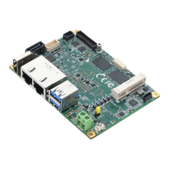
Summary of Contents for Asus AAEON PICO-TGU4
- Page 1 PICO-TGU4 PICO-ITX Single Board Computer with 11 Generation Intel® Core™ U processors User’s Manual 2 Last Updated: July 28, 2021...
- Page 2 Copyright Notice This document is copyrighted, 2021. All rights are reserved. The original manufacturer reserves the right to make improvements to the products described in this manual at any time without notice. No part of this manual may be reproduced, copied, translated, or transmitted in any form or by any means without the prior written permission of the original manufacturer.
- Page 3 Acknowledgement All other products’ name or trademarks are properties of their respective owners. Microsoft Windows® is a registered trademark of Microsoft Corp. ⚫ Intel®, Celeron® are registered trademarks of Intel Corporation ⚫ Core™ is a trademark of Intel Corporation ⚫ ITE is a trademark of Integrated Technology Express, Inc.
- Page 4 Packing List Before setting up your product, please make sure the following items have been shipped: Item Quantity PICO-TGU4 ⚫ If any of these items are missing or damaged, please contact your distributor or sales representative immediately. Preface...
- Page 5 About this Document This User’s Manual contains all the essential information, such as detailed descriptions and explanations on the product’s hardware and software features (if any), its specifications, dimensions, jumper/connector settings/definitions, and driver installation instructions (if any), to facilitate users in setting up their product. Users may refer to the product page on AAEON.com for the latest version of this document.
- Page 6 Safety Precautions Please read the following safety instructions carefully. It is advised that you keep this manual for future references All cautions and warnings on the device should be noted. Make sure the power source matches the power rating of the device. Position the power cord so that people cannot step on it.
- Page 7 If any of the following situations arises, please the contact our service personnel: Damaged power cord or plug Liquid intrusion to the device iii. Exposure to moisture Device is not working as expected or in a manner as described in this manual The device is dropped or damaged Any obvious signs of damage displayed on the device...
- Page 8 FCC Statement This device complies with Part 15 FCC Rules. Operation is subject to the following two conditions: (1) this device may not cause harmful interference, and (2) this device must accept any interference received including interference that may cause undesired operation.
- Page 9 China RoHS Requirements (CN) 产品中有毒有害物质或元素名称及含量 AAEON Main Board/ Daughter Board/ Backplane 有毒有害物质或元素 部件名称 铅 汞 镉 六价铬 多溴联苯 多溴二苯醚 (Pb) (Hg) (Cd) (Cr(VI)) (PBB) (PBDE) 印刷电路板 ○ ○ ○ ○ ○ ○ 及其电子组件 外部信号 ○ ○ ○ ○ ○ ○ 连接器及线材...
- Page 10 China RoHS Requirement (EN) Poisonous or Hazardous Substances or Elements in Products AAEON Main Board/ Daughter Board/ Backplane Poisonous or Hazardous Substances or Elements Hexavalent Polybrominated Polybrominated Component Lead Mercury Cadmium Chromium Biphenyls Diphenyl Ethers (Pb) (Hg) (Cd) (Cr(VI)) (PBB) (PBDE) PCB &...
-
Page 11: Table Of Contents
Table of Contents Chapter 1 - Product Specifications..................1 Specifications ......................2 Chapter 2 – Hardware Information ..................4 Dimensions ....................... 5 Jumpers and Connectors ..................6 List of Jumpers ......................7 2.3.1 Clear CMOS Jumper, Auto Power Button Selection (JP2) ....7 List of Connectors .................... - Page 12 Thermal Assembly Options ................. 28 2.6.1 Active Cooling Fan FAN01 ..............28 2.6.2 Fan-less Heatspreader HSP01 ............. 29 Chapter 3 - AMI BIOS Setup ....................30 System Test and Initialization ................31 AMI BIOS Setup ..................... 32 Setup Submenu: Main ..................33 Setup Submenu: Advanced .................
- Page 13 3.5.7 PCH-IO Configuration ................72 Setup Submenu: Security ..................73 3.6.1 Trusted Computing ................74 3.6.2 Secure Boot .................... 76 3.6.1.1 Key Management ..............77 Setup Submenu: Boot ..................79 3.7.1 BBS Priorities................... 80 Setup Submenu: Save & Exit ................81 Chapter 4 –...
- Page 14 This page left intentionally blank. Preface...
-
Page 15: Chapter 1 - Product Specifications
Chapter 1 Chapter 1 - Product Specifications... -
Page 16: Specifications
Specifications System Form Factor PICO-ITX 11th Generation Intel® Core™ i7/i5/i3/Celeron CPU Frequency Up to 4.8GHz Chipset Intel® Tiger Lake-UP3 SoC Processor Memory Type LPDDR4x 3200 MHz on board memory, In-Band ECC (select SKUs) Max. Memory Capacity Up to 32GB BIOS AMI UEFI Wake On LAN Watchdog Timer... - Page 17 Display 11th Generation Intel® Core™ i7/i5/i3/Celeron Chipset HDMI2.0b x 1, 4Kx2K 60Hz Resolution eDP x 1, up to HBR3, 8Kx4K 30Hz — LCD Interface Storage/SSD SATA III (6.0 Gbps) x 1 SATA Power (5V) x 1 Ethernet Intel® i225, 10/100/1000/2500Base, RJ45 x1 Intel®...
-
Page 18: Chapter 2 - Hardware Information
Chapter 2 Chapter 2 – Hardware Information... -
Page 19: Dimensions
Dimensions Chapter 2 – Hardware Information... -
Page 20: Jumpers And Connectors
Jumpers and Connectors Chapter 2 – Hardware Information... -
Page 21: List Of Jumpers
List of Jumpers Please refer to the table below for all of the board’s jumpers that you can configure for your application Label Function Clear CMOS Jumper, Auto Power Button Selection 2.3.1 Clear CMOS Jumper, Auto Power Button Selection (JP2) Clear CMOS Jumper Normal (Default) Clear CMOS... -
Page 22: List Of Connectors
List of Connectors Please refer to the table below for all of the board’s connectors that you can configure for your application Label Function HDMI Connector eDP Connector Mini Card Slot (Full Size) SATA Connector M.2 2280 M-Key Slot CN9-L Intel i225 2.5Gbps RJ-45 (Port A) CN9-R Intel i219 1Gbps RJ-45 (Port B) -
Page 23: Hdmi Port (Cn2)
2.4.1 HDMI Port (CN2) Pin Name Signal Type Signal Level HDMI1_TX2+ DIFF HDMI1_TX2- DIFF HDMI1_TX1+ DIFF HDMI1_TX1- DIFF HDMI1_TX0+ DIFF HDMI1_TX0- DIFF HDMI1_CLK+ DIFF HDMI1_CLK- DIFF DDC_CLK DDC_DATA Chapter 2 – Hardware Information... -
Page 24: Lvds/Edp (Reserved) (Cn3)
Pin Name Signal Type Signal Level HDMI1_HPD 2.4.2 LVDS/eDP (Reserved) (CN3) Pin Name Signal Type Signal Level +VDD +3.3V +VDD +3.3V +VDD +3.3V EDP_LANE2_DN DIFF EDP_LANE2_DP DIFF EDP_LANE1_DN DIFF EDP_LANE1_DP DIFF EDP_LANE0_DN DIFF EDP_LANE0_DP DIFF EDP_LANE3_DN DIFF EDP_LANE3_DP DIFF EDP_AUX_DN DIFF EDP_AUX_DP DIFF... -
Page 25: Mini-Card Slot (Full-Size) (Cn4)
Pin Name Signal Type Signal Level LVD1_DDC_DATA DDI0_BKLTEN_R DDI0_HPD +VCC_EDP_BKLT +12V (Default)/ +5V +VCC_EDP_BKLT +12V (Default)/ +5V +VCC_EDP_BKLT +12V (Default)/ +5V +VCC_EDP_BKLT +12V (Default)/ +5V 2.4.3 Mini-Card Slot (Full-Size) (CN4) Pin Name Signal Type Signal Level PCIE_WAKE# +3.3VSB +3.3V +1.5V +1.5V PCIE_CLK_REQ# UIM_PWR... - Page 26 Pin Name Signal Type Signal Level PCIE_REF_CLK+ DIFF UIM_RST UIM_VPP W_DISABLE# +3.3V PCIE_RST# +3.3V PCIE_RX- DIFF +3.3VSB +3.3V PCIE_RX+ DIFF +1.5V +1.5V SMB_CLK +3.3V PCIE_TX- DIFF SMB_DATA +3.3V PCIE_TX+ DIFF USB_D- DIFF USB_D+ DIFF Chapter 2 – Hardware Information...
-
Page 27: Sata Port (Cn5)
Pin Name Signal Type Signal Level +3.3VSB +3.3V +3.3VSB +3.3V +1.5V +1.5V +3.3VSB +3.3V 2.4.4 SATA Port (CN5) Pin Name Signal Type Signal Level SATA_TX+ DIFF SATA_TX- DIFF Chapter 2 – Hardware Information... -
Page 28: 2280 M-Key Slot (Cn8)
Pin Name Signal Type Signal Level SATA_RX- DIFF SATA_RX+ DIFF 2.4.5 M.2 2280 M-Key Slot (CN8) Pin Name Signal Type Signal Level +3.3V +3.3V +3.3V +3.3V PCIE3_RX- DIFF PCIE3_RX+ DIFF SATA_LED +3.3V PCIE3_TX- +3.3V +3.3V PCIE3_TX+ +3.3V +3.3V +3.3V +3.3V PCIE2_RX- DIFF +3.3V... - Page 29 Pin Name Signal Type Signal Level PCIE2_RX+ DIFF PCIE2_TX- DIFF PCIE2_TX+ DIFF PCIE1_RX- DIFF PCIE1_RX+ DIFF PCIE1_TX- DIFF PCIE1_TX+ DIFF DECSLP PCIE0_RX- DIFF PCIE0_RX+ DIFF Chapter 2 – Hardware Information...
- Page 30 Pin Name Signal Type Signal Level PCIE0_TX- DIFF PCIE0_TX+ DIFF PERST# PCIE_CLK_REQ# PCIE_CLK- DIFF PCIE_WAKE PCIE_CLK+ DIFF +3.3V +3.3V +3.3V +3.3V +3.3V +3.3V Chapter 2 – Hardware Information...
-
Page 31: Dual Lan (Rj-45) Intel I225 (Port A)/ Intel I219 (Port B) (Cn9)
2.4.6 Dual LAN (RJ-45) Intel i225 (Port A)/ Intel i219 (Port B) (CN9) Port A (i225) Port B (i219) Pin Name Pin Name LAN2_MDIO_P LAN1_MDIO_P LAN2_MDIO_N LAN1_MDIO_N LAN2_MDI1_P LAN1_MDI1_P LAN2_MDI1_N LAN1_MDI1_N 1CT5 2CT5 1CT6 2CT6 LAN2_MDI2_P LAN1_MDI2_P LAN2_MDI2_N LAN1_MDI2_N LAN2_MDI3_P LAN1_MDI3_P 1P10 LAN2_MDI3_N... -
Page 32: Dual Usb3.2 Gen 2 Ports (Port 1/ Port 2) (Cn10)
2.4.7 Dual USB3.2 Gen 2 Ports (Port 1/ Port 2) (CN10) Pin Name Signal Type Signal Level +5VSB USB0_D- DIFF USB0_D+ DIFF USB0_SSRX- DIFF USB0_SSRX+ DIFF USB0_SSTX- DIFF USB0_SSTX+ DIFF +5VSB USB1_D- DIFF USB1_D+ DIFF USB1_SSRX- DIFF USB1_SSRX+ DIFF USB1_SSTX- DIFF USB1_SSTX+ DIFF... -
Page 33: Spi Flash Programming Port (Cn15)
2.4.8 SPI Flash Programming Port (CN15) Pin Name Signal Type Signal Level SPI_MISO SPI_CLK +3.3VSB +3.3V SPI_MOSI SPI_CS Chapter 2 – Hardware Information... -
Page 34: Fan Connector (Cn16)
2.4.9 FAN Connector (CN16) Pin Name Signal Type Signal Level +V12S +12V TACH 2.4.10 eSPI Debug Port (CN17) Pin Name Signal Type Signal Level LAD0 +3.3V LAD1 +3.3V LAD2 +3.3V LAD3 +3.3V Chapter 2 – Hardware Information... -
Page 35: External Power Input (Cn18)
Pin Name Signal Type Signal Level +3.3V +3.3V LFRAME# LRESET# +3.3V LCLK SMB_DATA/ I2C_SDA SMB_CLK/ I2C_CLK SMB_ALERT/ SERIRQ +3.3V 2.4.11 External Power Input (CN18) +VIN GND Pin Name Signal Type Signal Level +VIN +12V Chapter 2 – Hardware Information... -
Page 36: Usb3.2 Gen 1 Dual Port Header (Cn21)
2.4.12 USB3.2 Gen 1 Dual Port Header (CN21) Pin Name Pin Name 5V_USB 5V_USB USB2_9_DN USB2_10_DN USB2_9_DP USB2_10_DP USB3_1_RXN USB3_4_RXN USB3_1_RXP USB3_4_RXP USB3_1_TXN USB3_4_TXN USB3_1_TXP USB3_4_TXP Chapter 2 – Hardware Information... -
Page 37: Dio 4Bit/ Com Dual Port/ Usb2.0 X 4 Header
2.4.13 DIO 4bit/ COM Dual Port/ USB2.0 x 4 Header Pin Name Pin Name DIO_0 DIO_1 DIO_2 DIO_3 DCD_1_CON DCD_2_CON RX_1_CON RX_2_CON TX_1_CON TX_2_CON DTR_1_CON DTR_2_CON DSR_1_CON DSR_2_CON RTS_1_CON RTS_2_CON CTS_1_CON CTS_2_CON RI_1_CON RI_2_CON Chapter 2 – Hardware Information... -
Page 38: Front Panel (Cn26)
Pin Name Pin Name 5V_USB 5V_USB USB2_5_DN USB2_6_DN USB2_5_DP USB2_6_DP 5V_USB 5V_USB USB2_7_DN USB2_8_DN USB2_7_DP USB2_8_DP 2.4.14 Front Panel (CN26) Pin Name Pin Name PWR_BTN- PWR_BTN+ HDD_LED- HDD_LED+ BUZZER- BUZZER+ PWR_LED- PWR_LED+ H/W RESET- H/W RESET+ Chapter 2 – Hardware Information... -
Page 39: Sata Power Connector (Cn29)
2.4.15 5V SATA Power Connector (CN29) Pin Name Signal Type Signal Level 2.4.16 RTC Battery Connector (CN30) Pin Name Signal Type Signal Level +3.3V +3.3V Chapter 2 – Hardware Information... -
Page 40: Dio 4Bit Port (Cn31)
2.4.17 DIO 4bit Port (CN31) Pin Name Signal Type Signal Level DIO_4 DIO_5 DIO_6 DIO_7 Chapter 2 – Hardware Information... -
Page 41: Function Block
Function Block Chapter 2 – Hardware Information... -
Page 42: Thermal Assembly Options
Thermal Assembly Options 2.6.1 Active Cooling Fan FAN01 Active Cooling Fan, Part Number: PICO-TGU4-FAN01 Chapter 2 – Hardware Information... -
Page 43: Fan-Less Heatspreader Hsp01
2.6.2 Fan-less Heatspreader HSP01 Heat spreader/ fan-less assembly, Part Number: PICO-TGU4-HSP01 Chapter 2 – Hardware Information... -
Page 44: Chapter 3 - Ami Bios Setup
Chapter 3 Chapter 3 - AMI BIOS Setup... -
Page 45: System Test And Initialization
System Test and Initialization The PICO-TGU4 uses certain routines to perform testing and initialization during the boot up sequence. If an error, fatal or non-fatal, is encountered, the system will output a few short beeps or display an error message. The board can usually continue the boot up sequence with non-fatal errors. -
Page 46: Ami Bios Setup
AMI BIOS Setup The AMI BIOS ROM has a pre-installed Setup program that allows users to modify basic system configurations. These configurations are stored in the battery-backed CMOS RAM and BIOS NVRAM so the information is retained when power is turned off. To enter BIOS Setup, turn on the system and immediately press <Del>... -
Page 47: Setup Submenu: Main
Setup Submenu: Main Chapter 3 – AMI BIOS Setup... -
Page 48: Setup Submenu: Advanced
Setup Submenu: Advanced Chapter 3 – AMI BIOS Setup... -
Page 49: Cpu Configuration
3.4.1 CPU Configuration Options Summary Intel (VMX) Disabled Virtualization Enabled Optimal Default, Failsafe Default Technology When enabled, a VMM can utilize the additional hardware capabilities provided by Vanderpool Technology. Intel(R) SpeedStep(tm) Disabled Enabled Optimal Default, Failsafe Default Allows more than two frequency ranges to be supported. Turbo Mode Disabled Enabled... -
Page 50: Memory Configuration
3.4.2 Memory Configuration Chapter 3 – AMI BIOS Setup... -
Page 51: Hardware Monitor
3.4.3 Hardware Monitor Options Summary Smart Fan Disabled Enabled Optimal Default, Failsafe Default Enable or Disable Smart Fan Chapter 3 – AMI BIOS Setup... -
Page 52: Smart Fan Mode Configuration
3.4.3.1 Smart Fan Mode Configuration Auto Duty-Cycle Mode Options Summary FAN1 Output Output PWM mode Mode (push pull) Linear Fan Application Output PWM mode Optimal Default, Failsafe Default (open drain) Output PWM mode (push pull) to control 4-wire fans. Linear fan application circuit to control 3-wire fan speed by fan’s power terminal. - Page 53 Options Summary Select the monitored temperature source for this fan. Duty Cycle Auto fan speed control. Fan speed will follow different temperature by different duty cycle 1-100 Temperature Manual Duty Mode Options Summary Manual Duty Mode Optimal Default, Failsafe Default Manual mode fan control, user can write expected duty cycle (PWM fan type) 1-100 Chapter 3 –...
-
Page 54: Pch-Fw Configuration
3.4.4 PCH-FW Configuration Chapter 3 – AMI BIOS Setup... -
Page 55: Firmware Update Configuration
3.4.4.1 Firmware Update Configuration Options Summary Me FW Image Re-Flash Disabled Optimal Default, Failsafe Default Enabled Enable/Disable Me FW Image Re-Flash function. FW Update Disabled Enabled Optimal Default, Failsafe Default Enable/Disable ME FW Update function. Chapter 3 – AMI BIOS Setup... -
Page 56: Nvme Configuration
3.4.5 NVMe Configuration Chapter 3 – AMI BIOS Setup... -
Page 57: Power Management
3.4.6 Power Management Options Summary Power Mode ATX Type Optimal Default, Failsafe Default AT Type Select system power mode Power Saving(ERP) Enabled Control Disabled Optimal Default, Failsafe Default Configure power mode for power saving function. Restore AC Power Loss Last State Optimal Default, Failsafe Default Always On Always Off... - Page 58 Options Summary Fixed Time: System will wake on the hr::min::sec specified. Dynamic Time: System will wake on the current time + Increase minute(s). Bypass: BIOS will not control RTC wake function during system shutdown Chapter 3 – AMI BIOS Setup...
-
Page 59: Aaeon Bios Robot
3.4.7 AAEON BIOS Robot Options Summary Sends watch dog before Disabled Optimal Default, Failsafe Default BIOS POST Enabled Enabled - Robot set Watch Dog Timer (WDT) right after power on, before BIOS start POST process. And then Robot will clear WDT on compeletion of POST. - Page 60 Options Summary Enabled - Robot set Watch Dog Timer (WDT) after POST completion, before BIOS transfer control to OS. WARNING: Before enabling this function, a program in OS must be in responsible for clearing WDT. Also, this function should be disabled if OS is going to update itself.
-
Page 61: Device Detecting Configuration
3.4.7.1 Device Detecting Configuration Options Summary Action Reset System Optimal Default, Failsafe Default Hold System Select action that robot should do. Soft or hard reset Soft Optimal Default, Failsafe Default Hard Select reset type robot should send on each boot. Retry-Count Optimal Default, Failsafe Default Fill retry counter here. - Page 62 Action: Hold System Options Summary Action Reset System Optimal Default, Failsafe Default Hold System Select action that robot should do. Holding time out Optimal Default, Failsafe Default (second) Fill hold time out here. Robot will hold system no longer then time-out value, and then let system continue its POST.
- Page 63 3.4.7.1.1 Device #X Detecting Configuration Interface: Disabled Options Summary Interface Disabled Optimal Default, Failsafe Default SMBUS Legacy I/O Super I/O MMIO Select interface robot should use to communicate with device. Chapter 3 – AMI BIOS Setup...
- Page 64 Interface: PCI Options Summary Optimal Default, Failsafe Default Fill BUS number to a PCI device, in hexadecimal. Range: 0 - FF Device Optimal Default, Failsafe Default Fill DEVICE number to a PCI device, in hexadecimal. Range: 0 - FF Function Optimal Default, Failsafe Default Fill FUNCTION number to a PCI device, in hexadecimal.
- Page 65 Options Summary Register data is bitwise equal to Optimal Default, Failsafe Default bytewise equal to bytewise lesser than bytewise larger than Select how robot should compare data read from register, to a value configured below. Register offset Optimal Default, Failsafe Default Fill register offset (or index) for robot to read, in hexadecimal.
- Page 66 Interface: DIO Options Summary Device Is not Optimal Default, Failsafe Default Select that robot should or should not do action if condition met. DIO pin number DIO1 Optimal Default, Failsafe Default DIO* Fill DIO pin number. 0 - DIO0, 1 - DIO1... and so on. For COM express product: 0-3 - GPI0-3, 4-7 - GPO0-3 Device Is not...
- Page 67 Interface: SMBUS Options Summary SMBUS Slave Optimal Default, Failsafe Default Address Fill slave address to a SMBUS device, in hexadecimal. Range: 0 - FF Device Is not Optimal Default, Failsafe Default Select that robot should or should not do action if condition met. In condition Present Optimal Default, Failsafe Default...
- Page 68 Options Summary Select how robot should compare data read from register, to a value configured below. Register offset Optimal Default, Failsafe Default Fill register offset (or index) for robot to read, in hexadecimal. Range: 0 - FF Bit offset Optimal Default, Failsafe Default Fill bit offset for register, for robot to compare with bit value.
- Page 69 Interface: Legacy I/O Options Summary I/O Address Optimal Default, Failsafe Default Fill I/O address device is responding to. Range: 0~FFFF Device Is not Optimal Default, Failsafe Default Select that robot should or should not do action if condition met. In condition Present Optimal Default, Failsafe Default Specified register data...
- Page 70 Options Summary Bit offset Optimal Default, Failsafe Default Fill bit offset for register, for robot to compare with bit value. Interface: Super I/O Options Summary Super I/O LDN Optimal Default, Failsafe Default Fill LDN number to a Super I/O device. Range: 0~FF Device Is not Optimal Default, Failsafe Default...
- Page 71 Options Summary bytewise equal to bytewise lesser than bytewise larger than Select how robot should compare data read from register, to a value configured below. Register offset Optimal Default, Failsafe Default Fill register offset (or index) for robot to read, in hexadecimal. Range: 0 - FF Bit offset Optimal Default, Failsafe Default Fill bit offset for register, for robot to compare with bit value.
- Page 72 Interface: MMIO Options Summary MMIO Address Optimal Default, Failsafe Default Fill Memory Mapped I/O address device is responding to. Range: 0~FFFFFFFF Device Is not Optimal Default, Failsafe Default Select that robot should or should not do action if condition met. In condition Present Optimal Default, Failsafe Default...
- Page 73 Options Summary Bit offset Optimal Default, Failsafe Default Fill bit offset for register, for robot to compare with bit value. Bit value Optimal Default, Failsafe Default High Fill bit value for robot to compare register-bit with specified offset. Byte value Optimal Default, Failsafe Default Fill a byte value for robot to compare register data with, in hexadecimal.
-
Page 74: Setup Submenu: System I/O
Setup Submenu: System I/O Chapter 3 – AMI BIOS Setup... -
Page 75: Pci Express Configuration
3.5.1 PCI Express Configuration Options Summary PCI Express Root Port Enabled Optimal Default, Failsafe Default Disabled Control the PCI Express Root Port. Chapter 3 – AMI BIOS Setup... -
Page 76: Storage Configuration
3.5.2 Storage Configuration Options Summary SATA Controller(s) Disabled Enabled Optimal Default, Failsafe Default Enable/Disable SATA Device. Port 1 Disabled Enabled Optimal Default, Failsafe Default Enable or Disable SATA Port Hot Plug Disabled Optimal Default, Failsafe Default Enabled Designates this port as Hot Pluggable. Chapter 3 –... -
Page 77: Hd Audio Subsystem Configuration Settings
3.5.3 HD Audio Subsystem Configuration Settings Options Summary HD Audio Disabled Enabled Optimal Default, Failsafe Default Control Detection of the HD-Audio device. Disabled = HDA will be unconditionally disabled Enabled = HDA will be unconditionally enabled Chapter 3 – AMI BIOS Setup... -
Page 78: Digital Io Port Configuration
3.5.4 Digital IO Port Configuration Options Summary DIO Port# Output Input Set DIO as Input or Output Output Level High Optimal Default, Failsafe Default Set output level when DIO pin is output Chapter 3 – AMI BIOS Setup... -
Page 79: Legacy Logical Devices Configuration
3.5.5 Legacy Logical Devices Configuration Chapter 3 – AMI BIOS Setup... -
Page 80: Serial Port 1 Configuration
3.5.5.1 Serial Port 1 Configuration Options Summary Use This Device Disable Enable Optimal Default, Failsafe Default Enable or Disable this Logical Device. Possible: Use Automatic Settings Optimal Default, Failsafe Default IO=3F8h; IRQ=4 IO=2F8h; IRQ=3 Allows user to change Device's Resource settings. New settings will be reflected on This Setup Page after System restarts. -
Page 81: Serial Port 2 Configuration
3.5.5.2 Serial Port 2 Configuration Options Summary Use This Device Disable Enable Optimal Default, Failsafe Default Enable or Disable this Logical Device. Possible: Use Automatic Settings Optimal Default, Failsafe Default IO=2F8h; IRQ=3 IO=3F8h; IRQ=4 Allows user to change Device's Resource settings. New settings will be reflected on This Setup Page after System restarts. -
Page 82: Serial Port Console Redirection
3.5.6 Serial Port Console Redirection Options Summary Console Redirection Disabled Optimal Default, Failsafe Default Enabled Console Redirection Enable or Disable. Console Redirection Disabled Optimal Default, Failsafe Default Enabled Console Redirection Enable or Disable. Chapter 3 – AMI BIOS Setup... -
Page 83: Console Redirection Settings
3.5.6.1 Console Redirection Settings Options Summary Terminal Type VT100 VT100+ VT-UTF8 ANSI Optimal Default, Failsafe Default Emulation: ANSI: Extended ASCII char set. VT100: ASCII char set. VT100+: Extends VT100 to support color, function keys, etc. VT-UTF8: Uses UTF8 encoding to map Unicode chars onto 1 or more bytes. Bits Per second 9600 19200... - Page 84 Options Summary Data Bits Optimal Default, Failsafe Default Parity None Optimal Default, Failsafe Default Even Mark Space A parity bit can be sent with the data bits to detect some transmission errors. Even: parity bit is 0 if the num of 1's in the data bits is even. Odd: parity bit is 0 if num of 1's in the data bits is odd.
- Page 85 Options Summary Putty KeyPad VT100 Optimal Default, Failsafe Default LINUX XTERMR6 ESCN VT400 Select FunctionKey and KeyPad on Putty. Chapter 3 – AMI BIOS Setup...
-
Page 86: Pch-Io Configuration
3.5.7 PCH-IO Configuration Options Summary MiniCard Slot Function SATA Optimal Default, Failsafe Default PCIe Select function enabled for Full size MiniCard Slot (CN6) Chapter 3 – AMI BIOS Setup... -
Page 87: Setup Submenu: Security
Setup Submenu: Security Change User/Administrator Password You can set an Administrator Password or User Password. An Administrator Password must be set before you can set a User Password. The password will be required during boot up, or when the user enters the Setup utility. A User Password does not provide access to many of the features in the Setup utility. -
Page 88: Trusted Computing
3.6.1 Trusted Computing Options Summary Security Device Disable Support Enable Optimal Default, Failsafe Default Enables or Disables BIOS support for security device. O.S. will not show Security Device. TCG EFI protocol and INT1A interface will not be available. SHA-1 PCR Bank Disable Enable Optimal Default, Failsafe Default... - Page 89 Options Summary Platform Hierarchy Disabled Enabled Optimal Default, Failsafe Default Enable or disable Platform Hierarchy Storage Hierarchy Disabled Enabled Optimal Default, Failsafe Default Enable or Disable Storage Hierarchy Endorsement Disabled Hierarchy Enabled Optimal Default, Failsafe Default Enable or Disable Endorsement Hierarchy TPM2.0 UEFI Spec TCG_1_2 Version...
-
Page 90: Secure Boot
3.6.2 Secure Boot Options Summary Secure Boot Disabled Optimal Default, Failsafe Default Enabled Secure Boot feature is Active if Secure Boot is Enabled, Platform Key (PK) is enrolled and the System is in User mode. The mode change requires platform reset Secure Boot Mode Custom... -
Page 91: Key Management
3.6.1.1 Key Management Options Summary Factory Key Provision Disabled Optimal Default, Failsafe Default Enabled Secure Boot feature is Active if Secure Boot is Enabled, Platform Key (PK) is enrolled and the System is in User mode. The mode change requires platform reset Restore Factory Keys Force System to User Mode. - Page 92 Options Summary Remove 'UEFI CA' from DB Device Guard ready system must not list 'Microsoft UEFI CA' Certificate in Authorized Signature database (db) Restore DB defaults Restore DB variable to factory defaults Platform Key (PK) Details Export Update Delete Key Exchange Keys Details Export Update...
-
Page 93: Setup Submenu: Boot
Setup Submenu: Boot Options Summary Quiet Boot Disabled Enabled Optimal Default, Failsafe Default Enable or disable showing boot logo. Network Stack Disabled Optimal Default, Failsafe Default Enabled Enable/Disable UEFI Network Stack Chapter 3 – AMI BIOS Setup... -
Page 94: Bbs Priorities
3.7.1 BBS Priorities Chapter 3 – AMI BIOS Setup... -
Page 95: Setup Submenu: Save & Exit
Setup Submenu: Save & Exit Chapter 3 – AMI BIOS Setup... -
Page 96: Chapter 4 - Drivers Installation
Chapter 4 Chapter 4 – Drivers Installation... -
Page 97: Drivers Download And Installation
Drivers Download and Installation Drivers for the PICO-TGU4 can be downloaded from the product page on the AAEON website by following this link: https://www.aaeon.com/en/p/pico-itx-turnkit-pico-tgu4 Download the driver(s) you need and follow the steps below to install them. Step 1 – Install Chipset Driver Open the Intel Chipset folder. - Page 98 Step 4 – Install Serial IO Driver Open the Serial IO folder. Run the SetupSerialIO.exe file Follow the instructions Driver will be installed automatically Step 5 – Install LAN Driver Open the LAN folder. Run the PROWinx64.exe file Follow the instructions Driver will be installed automatically Step 6 –...
-
Page 99: Appendix A - Mating Connectors
Appendix A Appendix A – Mating Connectors... -
Page 100: List Of Mating Connectors And Cables
List of Mating Connectors and Cables The following table lists mating connectors and available cables. Mating Connector Connector Available Function Cable P/N Label Cable Vendor Model no SSL20-30S eDP Cable 170X000313 Connector SATA Molex 887505318 SATA Cable 1709070460 Connector I2C/SMBUS/ I2C/SM BUS CN17 DebugConne... -
Page 101: Appendix B - I/O Information
Appendix B Appendix B - I/O Information... -
Page 102: I/O Address Map
I/O Address Map Appendix B – I/O Information... -
Page 103: Memory Address Map
Memory Address Map Appendix B – I/O Information... -
Page 104: Irq Mapping Chart
IRQ Mapping Chart Appendix B – I/O Information... - Page 105 Appendix B – I/O Information...
-
Page 106: Appendix C - Watchdog Timer Programming
Appendix C Appendix C - Watchdog Timer Programming... -
Page 107: Introduction To Watchdog Timer
Introduction to Watchdog Timer This section details how to set up and program the Watchdog Timer for your AAEON system or board. The watchdog timer is used to automatically detect malfunctions and recover the system. During normal operation, the system will regularly send a signal to reset the watchdog timer. -
Page 108: C.2 Programing The Watchdog Timer With Aaeon Sdk
C.2 Programing the Watchdog Timer with AAEON SDK If you have installed the AAEON Framework, you can program the Watchdog Timer using the AAEON SDK. Simply locate where the SDK is installed, and double click the icon. The following dialog box will appear: Count Mode: Set Watchdog Timer to count in minutes or seconds. -
Page 109: C.3 Programing Watchdog Timer With Aaeon Windows Eapi
C.3 Programing Watchdog Timer with AAEON Windows EAPI AAEON Framework (KMDF Driver) must be installed before calling these functions. EapiLibInitialize() should be the first to call before calling other EAPI functions. EApiLibUnInitialize() should be called to release resources before program exit. -
Page 110: Watchdog Timer Functions
EApiWDogStop must be called before Stage C/F to prevent event from being generated. EApiWDogStop must be called before Stage D/G to prevent system from being reset. C.3.1 Watchdog Timer Functions C.3.1.1 EapiWDogGetCap() Command Line: EApiWDogGetCap(…) __OUTOPT uint32_t *pMaxDelay, __OUTOPT uint32_t *pMaxEventTimeout, __OUTOPT uint32_t *pMaxResetTimeout Use this command to get maximum Supported Delay / Supported Event Timeout / Supported Reset Timeout of the watchdog timer. -
Page 111: Eapiwdogstart()
C.3.1.2 EapiWDogStart() Command Line: EApiWDogStart( __IN uint32_t Delay, __IN uint32_t Minute, __IN uint32_t EventTimeout, __IN uint32_t ResetTimeout Use this command to start the Watchdog Timer and set the timeout values. To stop the Watchdog Timer, issue the command EApiWDogStop. After issuing EAPiWDogStop, the command EApiWDogStart must be called again with new values to restart. -
Page 112: Eapiwdogtrigger()
C.3.1.3 EapiWDogTrigger() Command Line: EapiWDogTrigger() Use this command to trigger the Watchdog Timer. Parameters Function Parameters None Condition Return Values Library Uninitialized EAPI_STATUS_NOT_INITIALIZED Watchdog Not Started EAPI_STATUS_ERROR Common Error Common Error Code Others EAPI_STATUS_SUCCESS C.3.1.4 EapiWDogStop() Command Line: EapiWDogStop() Use this command to close the Watchdog Instance. This will disable the Watchdog Timer and clear previous settings. -
Page 113: Eapiwdogreloadtimer()
C.3.1.5 EapiWDogReloadTimer() Command Line: EapiWDogReloadTimer() Use this command to reload the Timeout count Parameters Function Parameters None Condition Return Values Library Uninitialized EAPI_STATUS_NOT_INITIALIZED Common Error Common Error Code Others EAPI_STATUS_SUCCESS C.3.1.6 EapiWDogGetStatus() Command Line: EapiWDogGetStatus( __OUTOPT uint32_t *pwdtMinute, __OUTOPT uint32_t *pwdtCountTime, __OUTOPT uint32_t *pwdtReloadTime Use this command to get the Watchdog Timer mode, time count value and reload timer. -
Page 114: Eapiwdogsetstatus
C.3.1.7 EapiWDogSetStatus() Command Line: EApiWDogSetStatus( __IN uint32_t wdtMinute, __IN uint32_t wdtCountTime, __IN uint32_t wdtReloadTime Use this command to set Watchdog Timer mode, time count value and reload timer. Parameters Function Parameters wdtMinute Set the mode of minute or second wdtCountTime Set WDT time count wdtReloadTime Set WDT ReloadTime...
Need help?
Do you have a question about the AAEON PICO-TGU4 and is the answer not in the manual?
Questions and answers