Table of Contents
Advertisement
Please refer to the original service manual for:
DVD Mechanism Unit (BRS12D), Order No. PSG1408009AE
Speaker system SB-VKX95GA-K, SB-VKW95GA-K, Order No. PSG1408002CE
TABLE OF CONTENTS
1 Safety Precautions----------------------------------------------- 3
1.1. General Guidelines---------------------------------------- 3
1.2. Before Repair and Adjustment ------------------------- 4
1.3. Protection Circuitry ---------------------------------------- 4
1.4. Caution For AC Cord (For GS only) ------------------ 5
1.5. Power Supply using SMPS ----------------------------- 6
1.6. Safety Parts Information --------------------------------- 6
2 Warning -------------------------------------------------------------- 7
to Electrostatically Sensitive (ES) Devices---------- 7
2.2. Precaution of Laser Diode------------------------------- 7
(PbF)---------------------------------------------------------- 8
2.4. Handling Precautions for Traverse Unit-------------- 8
Model No.
Product Color: (K)...Black Type
PAGE
3 Service Navigation --------------------------------------------- 10
3.1. Service Information -------------------------------------- 10
4 Specifications ---------------------------------------------------- 11
5 Location of Controls and Components------------------ 12
5.1. Remote Control Key Button Operation ------------- 12
5.2. Main Unit Key Button Operation---------------------- 13
6 Service Mode ----------------------------------------------------- 14
6.1. Service Mode Table ------------------------------------- 14
6.2. Sales Demonstration Lock Function ---------------- 15
6.3. Doctor Mode Table--------------------------------------- 16
6.4. Error Code Table ----------------------------------------- 19
6.5. Self-Diagnostic Mode ----------------------------------- 20
6.6. Self Diagnostic Function-Error Code---------------- 25
© Panasonic Corporation 2014. All rights reserved.
Unauthorized copying and distribution is a violation
of law.
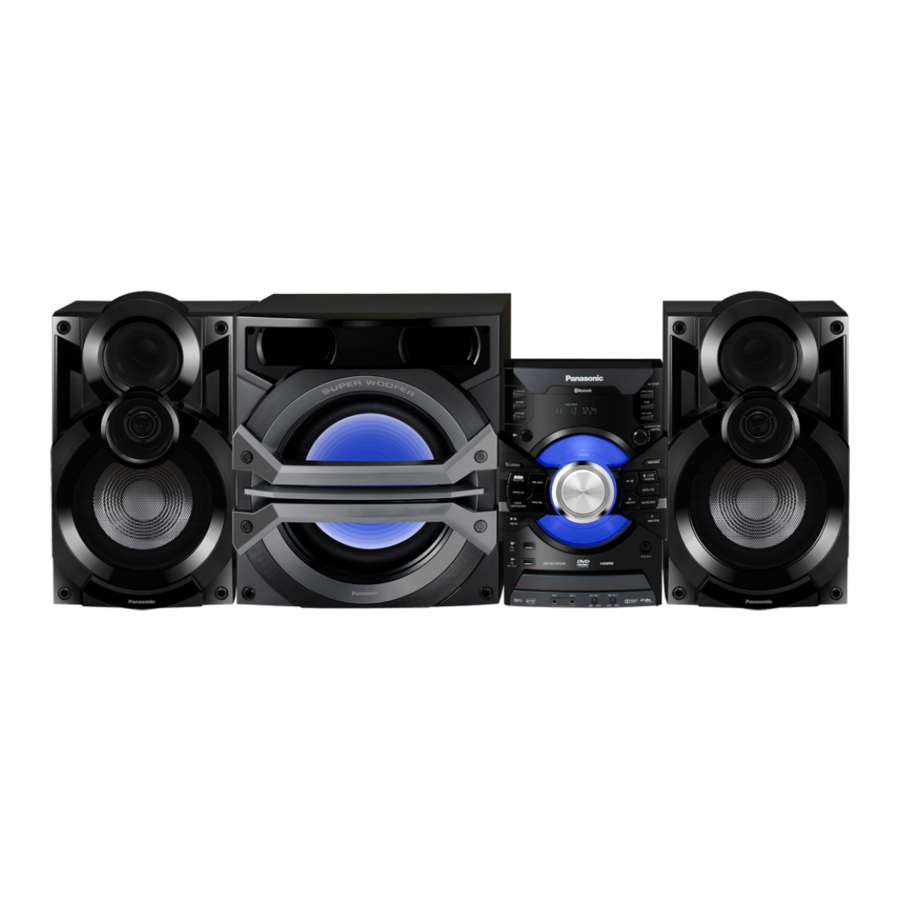
DVD Stereo System
SA-VKX95EE
SA-VKX95GA
SA-VKX95GS
electrostatic
PSG1408003CE
PAGE
breakdown
Advertisement
Table of Contents

Related Manuals for Panasonic SA-VKX95EE


Summary of Contents for Panasonic SA-VKX95EE
-
Page 1: Table Of Contents
6.4. Error Code Table ----------------------------------------- 19 2.4. Handling Precautions for Traverse Unit-------------- 8 6.5. Self-Diagnostic Mode ----------------------------------- 20 6.6. Self Diagnostic Function-Error Code---------------- 25 © Panasonic Corporation 2014. All rights reserved. Unauthorized copying and distribution is a violation of law. - Page 2 6.7. Firmware Version-Up Information -------------------- 26 13.4. Panel, USB & Music Port P.C.B. --------------------- 84 7 Troubleshooting Guide---------------------------------------- 29 13.5. Mic P.C.B.-------------------------------------------------- 85 7.1. No Power or No Display -------------------------------- 29 14 Voltage and Waveform Measurement-------------------- 87 7.2. Bluetooth Pairing Failure ------------------------------- 29 14.1.
-
Page 3: Safety Precautions
1 Safety Precautions 1.1. General Guidelines 1. IMPORTANT SAFETY NOTICE There are special components used in this equipment which are important for safety. These parts are marked by in the Schematic Diagrams, Circuit Board Layout, Exploded Views and Replacement Parts List. It is essential that these critical parts should be replaced with manufacturer’s specified parts to prevent X-RADIATION, shock, fire, or other hazards. -
Page 4: Before Repair And Adjustment
1.2. Before Repair and Adjustment Disconnect Power Supply AC to discharge AC capacitor as indicate below diagram (in SMPS Module) through a 10 , 10 W resis- tor to ground. Figure 1-2 Caution: DO NOT SHORT-CIRCUIT DIRECTLY (with a screwdriver blade, for instance), as this may destroy solid state devices. After repairs are completed, restore power gradually using a variac to avoid overcurrent. -
Page 5: Caution For Ac Cord (For Gs Only)
1.4. Caution For AC Cord (For GS only) Figure 1-3... -
Page 6: Power Supply Using Smps
1.5. Power Supply using SMPS This model uses Switching Mode Power Supply (SMPS) to provide the power supply to the unit. Here is the supplied part no. for the SMPS Module 1) N0AC2GP00002 Figure 1-4 1.6. Safety Parts Information Safety Parts List: There are special components used in this equipment which are important for safety. -
Page 7: Warning
2 Warning 2.1. Prevention of Electrostatic Discharge (ESD) to Electrostatically Sensi- tive (ES) Devices Some semiconductor (solid state) devices can be damaged easily by static electricity. Such components commonly are called Elec- trostatically Sensitive (ES) Devices. The following techniques should be used to help reduce the incidence of component damage caused by electrostatic discharge (ESD). -
Page 8: General Description About Lead Free Solder (Pbf)
Figure 2-1 2.3. General description about Lead Free Solder (PbF) The lead free solder has been used in the mounting process of all electrical components on the printed circuit boards used for this equipment in considering the globally environmental conservation. The normal solder is the alloy of tin (Sn) and lead (Pb). -
Page 9: Grounding For Prevention
3. The flexible cable may be cut off if an excessive force is applied to it. Use caution when handling the flexible cable. 4. The antistatic FFC is connected to the new optical pickup unit. After replacing the optical pickup unit and connecting the flexi- ble cable, cut off the antistatic FFC. -
Page 10: Service Navigation
3 Service Navigation 3.1. Service Information This service manual contains technical information which will allow service personnel’s to understand and service this model. Please place orders using the parts list and not the drawing reference numbers. If the circuit is changed or modified, this information will be followed by supplement service manual to be filed with original service manual. -
Page 11: Specifications
500 mA (max) analyzer. Bit rate Up to 4 Mbps (Xvid) USB Recording System: SC-VKX95EE-K Bit rate 128 kbps Main Unit: SA-VKX95EE-K USB recording speed Front Speakers: SB-VKX95GA-K Recording file format MP3 (*.mp3) Subwoofer: SB-VKW95GA-K ® Bluetooth section ... -
Page 12: Location Of Controls And Components
5 Location of Controls and Components 5.1. Remote Control Key Button Operation... -
Page 13: Main Unit Key Button Operation
5.2. Main Unit Key Button Operation... -
Page 14: Service Mode
6 Service Mode 6.1. Service Mode Table... -
Page 15: Sales Demonstration Lock Function
6.2. Sales Demonstration Lock Function... -
Page 16: Doctor Mode Table
6.3. Doctor Mode Table 6.3.1. Doctor Mode Table 1 Item Key Operation FL Display Mode Name Description Front Key Doctor Mode To enter into Doctor Mode In CD Mode: 1. Press [ ] button on main unit follow by [4] and [7] on remote control. - Page 17 6.3.2. Doctor Mode Table 2 Item Key Operation FL Display Mode Name Description Front Key Volume Setting To check the volume setting of the In Doctor Mode: Check main unit. 1. Press below button on the remote control. Press [7]: VOL50 Volume Press [8]: VOL35 Press [9]: VOL0...
- Page 18 6.3.3. Doctor Mode Table 3 Item Key Operation FL Display Mode Name Description Front Key Bluetooth Bluetooth module will need some 1. Go to Bluetooth selector and Version Check time to power up and read the then enter Doctor Mode. ( 2 sec) version display.
-
Page 19: Error Code Table
6.4. Error Code Table Self-Diagnostic Function provides information on any problems occurring for the unit and its respective components by displaying the error codes. These error code such as U**, H** and F** are stored in memory and held unless it is cleared. The error code is automatically display after entering into self-diagnostic mode. -
Page 20: Self-Diagnostic Mode
6.5. Self-Diagnostic Mode 6.5.1. Self-Diagnostic Mode Table 1 (For DVD Module) - Page 21 6.5.2. Self-Diagnostic Mode Table 2 (For DVD Module)
- Page 22 6.5.3. Self-Diagnostic Mode Table 3 (For DVD Module)
- Page 23 6.5.4. Self-Diagnostic Mode Table 4 (For DVD Module) Item FL Display Key Operation Mode Name Description Timer 1 check Timer 1 check In DVD/CD (no disc) Mode: (Display 1) Laser operation timer is measured Press [STOP] separately for DVD laser and CD laser. button on the main unit, and [ ] button on the...
- Page 24 6.5.5. Video Design Information Product Model Region TV Broadcasting Country Region Signal System Region Display Series Code System OSD Menu Language Default (Default) (Default) P, PC, USA, Canada, English (NA), Spanish (NA), NTSC NTSC (*A) English US Militry Canadian French Japan NTSC NTSC (*A)
-
Page 25: Self Diagnostic Function-Error Code
6.6. Self Diagnostic Function-Error Code 6.6.1. Mechanism Error Code Table 6.6.2. DVD Module Error Code Table... -
Page 26: Firmware Version-Up Information
6.7. Firmware Version-Up Information 6.7.1. Process Flow (1/3) Item FL/ GUI Display Remarks Process Description Collect ROM There are 2 files: User can put both files Files A) Syscon ROM file type: into the same root (Copy files into Display 1: directory. - Page 27 6.7.2. Process Flow (2/3) Item FL/ GUI Display Remarks Process Description GUI Display 1.3.2: GUI Display 1.3.2: UPDATING WRITING TO FLASHROM FL Display 2: Update stop Check Correct ROM files doesn't fit to the (Wrong ROM Type) ROM file type product type.
- Page 28 6.7.3. Process Flow (3/3) Item FL/ GUI Display Remarks Process Description 1. Update Failed Update software Update stop. FL Display 4: (Opecon) If Opecon software update fail: The theater set can't work, and can't be recovered by FL Display 3: "FAIL" . CD update again.
-
Page 29: Troubleshooting Guide
7 Troubleshooting Guide 7.1. No Power or No Display Caution: Check Primary E-Cap Press Power Button Check Secondary Cap. (C9 & C22) 1. AC Cord Plug-out No Display on (C1 & C2) of Unit or Remote Control Measured 38.5V FL Panel 2. -
Page 30: Usb Device Cannot Detect
7.5. USB Device Cannot Detect Press Power Button Press [SELECTOR and Press Play No Problem Plug-in USB Device choose USB mode] on the Set of Unit or Remote Control FL Display or Use Remote Control Found FL Display "USB" to Turn ON the Unit "Music Name or Title"... -
Page 31: No Output Sound
7.6. No Output Sound DVD/CD Play Press Power Button Press Play No Problem of Unit or Remote Control Output Sound DVD/CD Mode FL Display "Track & Count" Found to Turn ON the Unit Check CD Mechanism / Check Traverse Unit Main PCB Checking Points: 1) IC3001/IC3101/IC3201 (Digital Amplifier) - +12V, +36V... -
Page 32: Check Point
7.7. Check Point Power PCB Power PCB Pri. Cap Pri. Cap (CX1) (CX2) Fuse (F1) Sec. Cap. (C9) Sec. Cap. (C20) (0 ohm) C1 & C2 (150V) C9 & C20 (38.5V) - Page 33 Main PCB Main PCB IC2103_Pin#10 (15V) IC2107_Pin#3 (1.5V) IC2104_Pin#2 (3.3V) IC2108_Pin#2 (3.3V) Bluetooth CN2506_Pin#24 (5V) CN2506_Pin#20 (15V) CN2511 Pin#6 & Pin#7 (5V) Bluetooth 7.3 BACK-END PCB 7.3 BACK-END PCB IC7701_Pin 9 (5V)
-
Page 34: Disassembly And Assembly Instructions
8 Disassembly and Assembly Instructions • This section describes the disassembly and/or assembly procedures for all major printed circuit boards & main compo- nents for the unit. (You may refer to the section of “Main components and P.C.B Locations” as described in this service manual) •... -
Page 35: Main Components And P.c.b. Locations
8.3. Main Components and P.C.B. Locations... -
Page 36: Disassembly Of Top Cabinet
8.4. Disassembly of Top Cabinet 8.5. Disassembly of Front Panel Unit Step 1 Remove 4 screws. Step 2 Remove 5 screws. • Refer to “Disassembly of Top Cabinet”. Step 3 Release both sides of Top Cabinet outwards as arrow shown. Step 1 Detach 30P FFC at the connector (CN2506) on Main P.C.B. -
Page 37: Disassembly Of Panel P.c.b. And Music Port P.c.b
Step 8 Release tabs at bottom of unit. Step 3 Remove 7 screws. Step 9 Detach to remove Front Panel Unit Step 4 Release catches. 8.6. Disassembly of Panel P.C.B. and Music Port P.C.B. • Refer to “Disassembly of Top Cabinet”. •... -
Page 38: Disassembly Of Bluetooth P.c.b. Ass'y
8.7. Disassembly Bluetooth 8.8. Disassembly of USB P.C.B. P.C.B. Ass’y • Refer to “Disassembly of Top Cabinet”. • Refer to “Disassembly of Front Panel Unit”. • Refer to “Disassembly of Top Cabinet”. • Refer to “Disassembly of Front Panel Unit”. Step 1 Remove 1 screw. -
Page 39: Disassembly Of Rear Panel
Step 2 Remove 3 screws. Step 2 Release catch. Step 3 Remove Mic P.C.B.. Step 3 Remove fan unit. 8.10. Disassembly of Rear Panel. • Refer to “Disassembly of Top Cabinet”. Step 4 Lift up to remove Inner Chassis Unit. Step 1 Remove 11 screws. -
Page 40: Disassembly Of Main P.c.b. Ass'y
8.11. Disassembly of Main P.C.B. Step 9 Remove 4 screws. Ass’y • Refer to “Disassembly of Top Cabinet”. Step 1 Detach 30P FFC at the connector (CN2506) on Main P.C.B. Ass’y. Step 2 Detach 8P Cable at the connector (CN2511) on Main P.C.B. -
Page 41: Disassembly Of Smps Module
Step 12 Detach 30P FFC at the connector (FP5001) on Main Step 2 Detach 13P Cable at the connector (CON2) on SMPS P.C.B. Ass’y. Module. Step 13 Remove Main P.C.B. Ass’y. Step 3 Detach 2P Wire at the connector (CN2104) on Main P.C.B. -
Page 42: Disassembly Of Dvd Mechanism Unit
Step 6 Release P.C.B. Spacer. Step 2 Remove 1 screw. Step 7 Remove SMPS Module. Step 3 Release catches. Step 4 Lift up to remove Inner Chassis Unit. 8.13. Disassembly of DVD Mecha- nism Unit • Refer to “Disassembly of Top Cabinet”. •... -
Page 43: Disassembly Of Backend P.c.b. Ass'y
Step 5 Remove 2 screws. 8.14. Disassembly of Backend P.C.B. Ass’y • Refer to “Disassembly of Top Cabinet”. • Refer to “Disassembly of Front Panel Unit”. • Refer to “Disassembly of Main P.C.B. Ass’y”. • Refer to “Disassembly of DVD Mechanism Unit”. Step 1 Remove 2 screws. -
Page 44: Service Position
9 Service Position Note: For description of the disassembly procedures, see 9.2. Checking of Backend P.C.B. the Section 8. Ass'y 9.1. Checking of Panel P.C.B. and Step 1 Remove Top Cabinet. Main P.C.B. Ass'y Step 2 Remove Front Panel Unit. Step 3 Remove Main P.C.B. - Page 45 Step 12 Attach 5P Cable at the connector (CN2505) on Main Step 17 Attach 5P FFC at the connector (FP8252) on Backend P.C.B. Ass'y. P.C.B. Ass'y. Step 13 Attach 2P Wire at the connector (CN2104) on Main Step 18 Attach 6P FFC at the connector (FP8251) on Backend P.C.B.
-
Page 47: Block Diagram
LD CCW LD CCW LD CCW FP8101 FP5001 INNER SW INNER SW INNER SW FP8252 FP8101 FP5001 CLOSE SW CLOSE SW CLOSE SW CLOSE SW FP8252 FP8101 FP5001 OPEN SW OPEN SW OPEN SW OPEN SW SA-VKX95EE/GA/GS BACKEND (1/2) BLOCK DIAGRAM... - Page 48 USB2 D+ USB2 D+ 144 LOUT DAC2OUT 13 CBIN CN2505 FP9001 USB2 D- USB2 D- USB2 D- 146 ROUT DAC3OUT 15 CRIN FROM/TO SYSTEM CONTROL 5 MUTE1 Q2801 VMUTE FP5001 FP8101 VMUTE MUTING VMUTE CONTROL SA-VKX95EE/GA/GS BACKEND (2/2) BLOCK DIAGRAM...
-
Page 49: System Control
XOUT 11 OPEN SW OPEN SW IC2301 C3EBFY000030 VMUTE VMUTE EEPROM DVD CMD DV5 CMD EDA 33 5 SDA ECK 34 6 SCL IC2300 RFKWMVKX95GM MICROPROCESSOR NOTE: “ * ” REF IS FOR INDICATION ONLY SA-VKX95EE/GA/GS SYSTEM CONTROL (1/3) BLOCK DIAGRAM... - Page 50 D6203 KEY-CON KARAOKE D6208 S6213 S6218 MANUAL EQ PLAY/PAUSE S6224 S6219 ECHO D6204 RADIO/AUX D6209 S6214 D.BASS -SUPER WOOFER S6220 D6210 DVD/CD SG10 S6225 VOCAL CANCEL D6205 S6215 TO SYSTEM CONTROL REC/PAUSE BLOCK (1/3) SA-VKX95EE/GA/GS SYSTEM CONTROL (2/3) BLOCK DIAGRAM...
- Page 51 I2C SCL I2C SCL NRST NRST I2C SDA I2C SDA SYNC SYNC DSP ERR DSP ERR PDET DC DET PWR TUN INT TUN INT TUN SDO TUN SDO SOC MCLK SOC MCLK ILLUMINATION ILLUMINATION SA-VKX95EE/GA/GS SYSTEM CONTROL (3/3) BLOCK DIAGRAM...
-
Page 52: Audio
TO AM ANTENNA GPIO2 18 TUN INT TUN RST FROM/TO SYSTEM CONTROL DFS 14 TUN WCK DCLK 17 TUN BCK I2C SCL SCLK I2C SDA SDIO NOTE: “ * ” REF IS FOR INDICATION ONLY SA-VKX95EE/GA/GS AUDIO (1/3) BLOCK DIAGRAM... - Page 53 TO AUDIO BLOCK (3/3) 46 SDO1 5 SDI1 48 MCK OUT 13 XIN X4801 14 XOUT SOC MCLK FROM/TO DSP ERR 19 IRQ N SYSTEM CONTROL DSP RESET2 11 IC N I2C SCL I2C SDA SA-VKX95EE/GA/GS AUDIO (2/3) BLOCK DIAGRAM...
- Page 54 INPUT A BST A INPUT B OUT A OUT A OUT B BST B BST C JK3501 /RST OUT C FRONT LEFT TO AUDIO JK3501 OUT D BLOCK (2/3) OUT D /OTW /FAULT BST D SA-VKX95EE/GA/GS AUDIO (3/3) BLOCK DIAGRAM...
-
Page 55: Power Supply
1 CN +1.8V VO 3 +1.8V +3.3V 4 VIN CN2103 PCONT PCONT CN2103 SMPS BP SMPS BP FROM/TO CN2103 SMPS ID SYSTEM CONTROL SMPS ID TO POWER SUPPLY CN2103 TEMP DET BLOCK (2/2) TEMP DET SA-VKX95EE/GA/GS POWER SUPPLY (1/2) BLOCK DIAGRAM... - Page 56 +1.2V PW DVD +3R3V PW DVD +3R3V 3 VCC D+3.3V 6 +3.3V NRESET NRESET NRESET RST O 2 TO BACKEND TO POWER SUPPLY BLOCK (1/2) NOTE: “ * ” REF IS FOR INDICATION ONLY SA-VKX95EE/GA/GS POWER SUPPLY (2/2) BLOCK DIAGRAM...
-
Page 57: Wiring Connection Diagram
FP8252 FP8101 TO LOADING P.C.B. FP8531 (DVD MECHANISM UNIT) FP8251 6P MUSIC PORT P.C.B. TO TRAVERSE P.C.B. (DVD MECHANISM UNIT) TO OPTICAL PICKUP UNIT (DVD MECHANISM UNIT) NOTE: " * " REF IS FOR INDICATION ONLY. SA-VKX95EE/GA/GS WIRING CONNECTION DIAGRAM... -
Page 59: Schematic Diagram
12 Schematic Diagram 12.1. Schematic Diagram Notes : AUX/Music Port/Mic Audio input signal line : AM signal line • This schematic diagram may be modified at any time : FM signal line with the development of new technology. Notes: S6200: Power ( ) switch. -
Page 61: Backend (Dv5U) Circuit (1/4)
DV: BACKEND (DV5U): SCHEMATIC DIAGRAM - 1 ~ 4 D1H41032A014 MD: BACKEND (MOTOR DRIVER): SCHEMATIC DIAGRAM - 5 VI: BACKEND (VIDEO): SCHEMATIC DIAGRAM - 6 HD: BACKEND (HDMI): SCHEMATIC DIAGRAM - 7 C8505 RX8031 D1H44722A014 TO BACKEND (DV5U) CIRCUIT (3/4) SA-VKX95EE/GA/GS BACKEND (DV5U) CIRCUIT... -
Page 62: Backend (Dv5U) Circuit (2/4)
DV: BACKEND (DV5U): SCHEMATIC DIAGRAM - 1 ~ 4 TO BACKEND (DV5U) MD: BACKEND (MOTOR DRIVER): SCHEMATIC DIAGRAM - 5 CIRCUIT (4/4) VI: BACKEND (VIDEO): SCHEMATIC DIAGRAM - 6 SA-VKX95EE/GA/GS BACKEND (DV5U) CIRCUIT HD: BACKEND (HDMI): SCHEMATIC DIAGRAM - 7... -
Page 63: Backend (Dv5U) Circuit (3/4)
FLASH MEMORY IC8051 C3ABPY000090 SDRAM DV: BACKEND (DV5U): SCHEMATIC DIAGRAM - 1 ~ 4 MD: BACKEND (MOTOR DRIVER): SCHEMATIC DIAGRAM - 5 VI: BACKEND (VIDEO): SCHEMATIC DIAGRAM - 6 SA-VKX95EE/GA/GS BACKEND (DV5U) CIRCUIT HD: BACKEND (HDMI): SCHEMATIC DIAGRAM - 7... -
Page 64: Backend (Dv5U) Circuit (4/4)
0.082 DRV1 R8232 5.6K SP_DRV DV: BACKEND (DV5U): SCHEMATIC DIAGRAM - 1 ~ 4 MD: BACKEND (MOTOR DRIVER): SCHEMATIC DIAGRAM - 5 VI: BACKEND (VIDEO): SCHEMATIC DIAGRAM - 6 SA-VKX95EE/GA/GS BACKEND (DV5U) CIRCUIT HD: BACKEND (HDMI): SCHEMATIC DIAGRAM - 7... -
Page 65: Backend (Motor Driver) Circuit
D_GND IC8252 C0ABGA000090 OP-AMP DV: BACKEND (DV5U): SCHEMATIC DIAGRAM - 1 ~ 4 MD: BACKEND (MOTOR DRIVER): SCHEMATIC DIAGRAM - 5 VI: BACKEND (VIDEO): SCHEMATIC DIAGRAM - 6 SA-VKX95EE/GA/GS BACKEND (MOTOR DRIVER) CIRCUIT HD: BACKEND (HDMI): SCHEMATIC DIAGRAM - 7... -
Page 66: Backend (Video) Circuit
R3806 CRIN CROUT VCC2 CRSAG DV: BACKEND (DV5U): SCHEMATIC DIAGRAM - 1 ~ 4 MD: BACKEND (MOTOR DRIVER): SCHEMATIC DIAGRAM - 5 VI: BACKEND (VIDEO): SCHEMATIC DIAGRAM - 6 SA-VKX95EE/GA/GS BACKEND (VIDEO) CIRCUIT HD: BACKEND (HDMI): SCHEMATIC DIAGRAM - 7... -
Page 67: Backend (Hdmi) Circuit
C3956 I2C_SDA K3903 PW_M_+9V C3954 DV: BACKEND (DV5U): SCHEMATIC DIAGRAM - 1 ~ 4 MD: BACKEND (MOTOR DRIVER): SCHEMATIC DIAGRAM - 5 VI: BACKEND (VIDEO): SCHEMATIC DIAGRAM - 6 SA-VKX95EE/GA/GS BACKEND (HDMI) CIRCUIT HD: BACKEND (HDMI): SCHEMATIC DIAGRAM - 7... -
Page 68: Main (Up) Circuit
TU: MAIN (TUNER AUX): SCHEMATIC DIAGRAM - 11 DS: MAIN (DSP): SCHEMATIC DIAGRAM - 12 ~ 13 DA: MAIN (DAMP): SCHEMATIC DIAGRAM - 14 ~ 15 VR: MAIN (VREG FAN): SCHEMATIC DIAGRAM - 16 ~ 17 SA-VKX95EE/GA/GS MAIN (UP) CIRCUIT CN: MAIN (CONNECTOR): SCHEMATIC DIAGRAM - 18... -
Page 69: Main (Soc) Circuit
DS: MAIN (DSP): SCHEMATIC DIAGRAM - 12 ~ 13 PW_+36V ADAC_MUTE QR1001 DA: MAIN (DAMP): SCHEMATIC DIAGRAM - 14 ~ 15 ADAC_MUTE ILLUMINATION B1GBCFJJ0040 VR: MAIN (VREG FAN): SCHEMATIC DIAGRAM - 16 ~ 17 ILLUMINATION SWITCH CN: MAIN (CONNECTOR): SCHEMATIC DIAGRAM - 18 SA-VKX95EE/GA/GS MAIN (SOC) CIRCUIT... -
Page 70: Main (Usb) Circuit
TU: MAIN (TUNER AUX): SCHEMATIC DIAGRAM - 11 DS: MAIN (DSP): SCHEMATIC DIAGRAM - 12 ~ 13 DA: MAIN (DAMP): SCHEMATIC DIAGRAM - 14 ~ 15 VR: MAIN (VREG FAN): SCHEMATIC DIAGRAM - 16 ~ 17 SA-VKX95EE/GA/GS MAIN (USB) CIRCUIT CN: MAIN (CONNECTOR): SCHEMATIC DIAGRAM - 18... -
Page 71: Main (Tuner Aux) Circuit
DS: MAIN (DSP): SCHEMATIC DIAGRAM - 12 ~ 13 DA: MAIN (DAMP): SCHEMATIC DIAGRAM - 14 ~ 15 VR: MAIN (VREG FAN): SCHEMATIC DIAGRAM - 16 ~ 17 SA-VKX95EE/GA/GS MAIN (TUNER AUX) CIRCUIT CN: MAIN (CONNECTOR): SCHEMATIC DIAGRAM - 18... -
Page 72: Main (Dsp) Circuit (1/2)
TU: MAIN (TUNER AUX): SCHEMATIC DIAGRAM - 11 DS: MAIN (DSP): SCHEMATIC DIAGRAM - 12 ~ 13 DA: MAIN (DAMP): SCHEMATIC DIAGRAM - 14 ~ 15 VR: MAIN (VREG FAN): SCHEMATIC DIAGRAM - 16 ~ 17 SA-VKX95EE/GA/GS MAIN (DSP) CIRCUIT CN: MAIN (CONNECTOR): SCHEMATIC DIAGRAM - 18... -
Page 73: Main (Dsp) Circuit (2/2)
TU: MAIN (TUNER AUX): SCHEMATIC DIAGRAM - 11 DS: MAIN (DSP): SCHEMATIC DIAGRAM - 12 ~ 13 DA: MAIN (DAMP): SCHEMATIC DIAGRAM - 14 ~ 15 VR: MAIN (VREG FAN): SCHEMATIC DIAGRAM - 16 ~ 17 SA-VKX95EE/GA/GS MAIN (DSP) CIRCUIT CN: MAIN (CONNECTOR): SCHEMATIC DIAGRAM - 18... -
Page 74: Main (Damp) Circuit (1/2)
TU: MAIN (TUNER AUX): SCHEMATIC DIAGRAM - 11 DS: MAIN (DSP): SCHEMATIC DIAGRAM - 12 ~ 13 DA: MAIN (DAMP): SCHEMATIC DIAGRAM - 14 ~ 15 VR: MAIN (VREG FAN): SCHEMATIC DIAGRAM - 16 ~ 17 SA-VKX95EE/GA/GS MAIN (DAMP) CIRCUIT CN: MAIN (CONNECTOR): SCHEMATIC DIAGRAM - 18... -
Page 75: Main (Damp) Circuit (2/2)
TU: MAIN (TUNER AUX): SCHEMATIC DIAGRAM - 11 DS: MAIN (DSP): SCHEMATIC DIAGRAM - 12 ~ 13 DA: MAIN (DAMP): SCHEMATIC DIAGRAM - 14 ~ 15 VR: MAIN (VREG FAN): SCHEMATIC DIAGRAM - 16 ~ 17 SA-VKX95EE/GA/GS MAIN (DAMP) CIRCUIT CN: MAIN (CONNECTOR): SCHEMATIC DIAGRAM - 18... -
Page 76: Main (Vreg Fan) Circuit (1/2)
DS: MAIN (DSP): SCHEMATIC DIAGRAM - 12 ~ 13 DA: MAIN (DAMP): SCHEMATIC DIAGRAM - 14 ~ 15 VR: MAIN (VREG FAN): SCHEMATIC DIAGRAM - 16 ~ 17 SA-VKX95EE/GA/GS MAIN (VREG FAN) CIRCUIT CN: MAIN (CONNECTOR): SCHEMATIC DIAGRAM - 18... -
Page 77: Main (Vreg Fan) Circuit (2/2)
DA: MAIN (DAMP): SCHEMATIC DIAGRAM - 14 ~ 15 VR: MAIN (VREG FAN): SCHEMATIC DIAGRAM - 16 ~ 17 ZJ2100 CN: MAIN (CONNECTOR): SCHEMATIC DIAGRAM - 18 NOTE: “ * ” REF IS FOR INDICATION ONLY SA-VKX95EE/GA/GS MAIN (VREG FAN) CIRCUIT... -
Page 78: Main (Connector) Circuit
DIAGRAM - 19 DS: MAIN (DSP): SCHEMATIC DIAGRAM - 12 ~ 13 DA: MAIN (DAMP): SCHEMATIC DIAGRAM - 14 ~ 15 VR: MAIN (VREG FAN): SCHEMATIC DIAGRAM - 16 ~ 17 SA-VKX95EE/GA/GS MAIN (CONNECTOR) CIRCUIT CN: MAIN (CONNECTOR): SCHEMATIC DIAGRAM - 18... -
Page 79: Panel Circuit
S6218 S6219 S6220 BLUETOOTH/USB DJ JUKEBOX ALBUM/TRACK LOCAL KEY-CON MANUAL EQ ECHO D.BASS VOCAL CANCEL FL DISPLAY DIMMER KARAOKE PLAY/PAUSE RADIO/AUX DVD/CD -PAIRING PRESET EQ -SUPER WOOFER REC/PAUSE NOTE: “ * ” REF IS FOR INDICATION ONLY SA-VKX95EE/GA/GS PANEL CIRCUIT... -
Page 80: Usb, Music Port & Mic Circuit
IN SCHEMATIC DIAGRAM - 19 C6323 0.01 L6302 J0JBC0000019 R6301 AUX IN 2 ZJ6301 L6301 J0JBC0000019 CHASSIS_GND TO CHASSIS GND CHASSIS_GND L6300 J0JBC0000019 NOTE: “ * ” REF IS FOR INDICATION ONLY SA-VKX95EE/GA/GS USB / MUSIC PORT / MIC CIRCUIT... -
Page 81: Printed Circuit Board
(TO OPTICAL PICKUP UNIT R8263 (DVD MECHANISM LB8561 LB8258 UNIT BRS12D)) Q8551 Q8552 Q8562 LB8257 FP8251 R8268 LB8256 (TO TRAVERSE PCB IC8252 (DVD MECHANISM R8562 UNIT BRS12D)) R8568 R8269 Q8561 R8558 R8270 (SIDE A) (SIDE B) SA-VKX95EE/GA/GS BACKEND P.C.B. ASS’Y... -
Page 82: Main P.c.b. Ass'y (Side A)
R3536 Q3502 IC2107 C3533 C3529 C3538 C3537 C3530 C3534 Q3500 Q3501 R2235 Q2117 QR2102 R2201 R2215 R2200 R6113 C3567 R2241 R6116 C6109 R3525 R6136 C3568 LB2543 R2227 C6108 R3526 LB2544 C2183 R6112 C2186 LB2545 (SIDE A) SA-VKX95EE/GA/GS MAIN P.C.B. ASS’Y... -
Page 83: Main P.c.b. Ass'y (Side B)
(TO FAN (INNER)) VA51 JK52 1-SW+ 3-FR+ 5-FL+ 4-GND 2-SW- 4-FR- 6-FL- 1-GND CN2504 (TO SB-VKX95) (SUBWOOFER)) TO SPEAKERS AUX IN 1 FM ANT AM ANT (SIDE B) SA-VKX95EE/GA/GS NOTE: " * " REF IS FOR INDICATION ONLY MAIN P.C.B. ASS’Y... -
Page 84: Panel, Usb & Music Port P.c.b
13.4. Panel, USB & Music Port P.C.B. PANEL P.C.B. (REP5139AA) USB P.C.B. (REP5139AB) CN6401 S6225 S6226 (VOCAL CANCEL) 5 4 3 (FL DISPLAY) JK6401 JK6400 C6030 C6028 FL6000 W200 USB PORT B USB PORT A S6224 S6227 C6027 IR6500 REC/PLAY PLAY (ECHO) (DIMMER) -
Page 85: Mic P.c.b
13.5. Mic P.C.B. MIC P.C.B. (REP5110A) ZJ1403 (TO CHASSIS GND) R1423 R1422 C1430 CN1401 R1415 C1402 IC1400 C1442 C1425 R1405 TP1401 IC1401 R1401 C1406 R1414 R1418 R1406 C1407 C1426 R1419 R1402 R1411 JK1401 JK1403 R1407 R1400 R1408 LB1400 R1403 LB1404 C1400 C1417 CK6002... -
Page 87: Voltage And Waveform Measurement
14 Voltage and Waveform Measurement 14.1. Voltage Measurement Note: • Indication Voltage Values are in standard values for the unit measured by the DC electronic circuit tester (high-impedance) with the chassis taken as standard. Therefore, there may exist some errors in voltage values, depending on the internal impedance of the DC circuit tester. •... - Page 88 14.1.2. Backend P.C.B. Ass'y (2/4) IC8001 REF NO. MODE PLAY STANDBY IC8001 REF NO. MODE PLAY STANDBY IC8001 REF NO. MODE PLAY STANDBY REF NO. IC8001 MODE PLAY STANDBY IC8001 REF NO. MODE PLAY STANDBY IC8001 REF NO. MODE PLAY STANDBY IC8001 REF NO.
- Page 89 14.1.3. Backend P.C.B. Ass'y (3/4) IC8051 REF NO. MODE PLAY STANDBY IC8051 REF NO. MODE PLAY STANDBY IC8111 REF NO. MODE PLAY STANDBY IC8251 REF NO. MODE PLAY STANDBY IC8251 REF NO. MODE PLAY STANDBY IC8252 REF NO. MODE PLAY STANDBY IC8701 REF NO.
- Page 90 14.1.4. Backend P.C.B. Ass'y (4/4) REF NO. Q8561 Q8562 Q8563 Q8564 Q8565 MODE PLAY STANDBY SA-VKX95GA/GS/EE BACKEND P.C.B. ASS'Y...
- Page 91 14.1.5. Main P.C.B. Ass'y (1/5) IC1001 REF NO. MODE PLAY STANDBY REF NO. IC1001 MODE PLAY STANDBY IC1001 REF NO. MODE PLAY STANDBY IC1001 REF NO. MODE PLAY STANDBY IC1001 REF NO. MODE PLAY STANDBY IC1001 REF NO. MODE PLAY STANDBY IC1001 REF NO.
- Page 92 14.1.6. Main P.C.B. Ass'y (2/5) IC2103 REF NO. MODE PLAY 21.3 39.5 15.2 STANDBY 21.3 39.5 15.2 REF NO. IC2104 MODE PLAY STANDBY IC2105 REF NO. MODE PLAY 15.4 STANDBY 15.4 IC2107 REF NO. MODE PLAY STANDBY IC2108 REF NO. MODE PLAY STANDBY...
- Page 93 14.1.7. Main P.C.B. Ass'y (3/5) IC3001 REF NO. MODE PLAY 30.1 STANDBY 30.1 REF NO. IC3101 MODE PLAY 12.2 12.1 STANDBY 12.2 12.1 IC3101 REF NO. MODE PLAY 30.1 30.1 39.5 39.5 39.5 39.5 39.5 39.5 STANDBY 30.1 30.1 39.5 39.5 39.5 39.5 39.5 39.5 IC3101 REF NO.
- Page 94 14.1.8. Main P.C.B. Ass'y (4/5) IC4803 REF NO. MODE PLAY STANDBY REF NO. IC4803 MODE PLAY 16.8 16.8 16.8 16.8 STANDBY 16.8 16.8 16.8 16.8 IC4803 REF NO. MODE PLAY STANDBY IC4804 REF NO. MODE PLAY STANDBY IC6100 REF NO. MODE PLAY 12.5 12.5...
- Page 95 14.1.9. Main P.C.B. Ass'y (5/5) , Mic & Panel P.C.B. Q3503 Q9004 QR2102 QR2502 QR2503 REF NO. MODE PLAY STANDBY QR2505 QR6101 QR9002 REF NO. MODE PLAY 12.2 STANDBY 12.2 SA-VKX95GA/GS/EE MAIN P.C.B. ASS'Y IC1400 REF NO. MODE PLAY 12.3 12.3 STANDBY 12.3...
-
Page 97: Exploded View And Replacement Parts List
ZJ6301 CN6300 *P7701 (USB P.C.B.) *(BLUETOOTH P.C.B. ASS'Y) JK6400 JK6301 (MUSIC PORT P.C.B.) CN6401 JK6401 (MIC P.C.B.) JK1403 CN1401 JK1401 ZJ1403 VR1400 VR1401 NOTE: " * " PART IS NOT SUPPLIED / REF IS FOR INDICATION ONLY. SA-VKX95EE/GA/GS-K CABINET DRAWING... -
Page 98: Cabinet Parts Location
CN2507 CN2103 CN2003 P1002 ZJ2100 FP5001 ZJ2102 (SMPS MODULE) (DVD MECHANISM UNIT) P3901 FP9001 FP8031 JK3801 (BACKEND P.C.B. ASS'Y) FP8101 FP8252 FP8531 FP8251 SA-VKX95EE/GA/GS-K CABINET DRAWING NOTE: " * " PART IS NOT SUPPLIED / REF IS FOR INDICATION ONLY. -
Page 99: Packaging
15.3. Packaging ACCESSORIES BAG (FOR GS ONLY) REMOTE CONTROL AC CORD **SPACER PAD SA-VKX95EE/GA/GS SB-VKX95GA AC CORD (FOR GA ONLY) OI BOOK SB-VKW95GA FM INDOOR ANTENNA AM LOOP ANTENNA **LAYER PAD HDMI CABLE VIDEO CABLE F R O N T... -
Page 101: Mechanical Replacement Part List
15.4. Mechanical Replacement Part List Safety Ref. Part No. Part Name & Qty Remarks Description RGW0446-1S VOLUME KNOB Safety Ref. Part No. Part Name & Qty Remarks Description RGW0435-K SKIP KNOB RHD26043-1 SCREW CABINET RHD26046-L SCREW CHASSIS RHD30007-K2J SCREW RHD30111-31 SCREW REE1999 (MAIN-... - Page 102 Safety Ref. Part No. Part Name & Qty Remarks Description RSC1296 MIC PCB SHIELD L6FALEFH0030 FAN UNIT RMKX1016-4 FAN FIXTURE RHDX30005-J SCREW REE1743 12P FFC (PANEL- BLUETOOTH) RMX0510 SMPS PCB SPACER XTW3+30TFJ SCREW RGW0450-K MIC VOLUME KNOB RHD26016-1L SCREW RMA2526 SHIELD PLATE RMX0524 PCB SPACER...
-
Page 103: Electrical Replacement Parts List
15.5. Electrical Replacement Parts List Safety Ref. Part No. Part Name & Qty Remarks Description Safety Ref. Part No. Part Name & Qty Remarks IC1003 RFKWFVKX95GM (E.S.D) Description JIGS & PRINTED CIRCUIT IC1004 RFKWEVKX95GM (E.S.D) BOARDS JIGS & IC1005 C0JBAR000596 (E.S.D) PCB1 RFKB5103EA... - Page 104 Safety Ref. Part No. Part Name & Qty Remarks Safety Ref. Part No. Part Name & Qty Remarks Description Description IC8111 C0DBFZG00001 (E.S.D) D2104 DZ2J130M0L DIODE (E.S.D) IC8251 C0GBY0000117 (E.S.D) D2105 B0ADDJ000032 DIODE (E.S.D) IC8252 C0ABGA000090 (E.S.D) D2106 B0JCPG000032 DIODE (E.S.D) IC8611 RFKB5104A...
- Page 105 Safety Ref. Part No. Part Name & Qty Remarks Safety Ref. Part No. Part Name & Qty Remarks Description Description S6226 EVQ21405RJ SW FL DISPLAY LB1005 J0JYC0000656 INDUCTOR S6227 EVQ21405RJ SW DIMMER LB1006 J0JBC0000010 INDUCTOR S6228 EVQ21405RJ SW KARAOKE LB1007 J0JBC0000010 INDUCTOR LB1008...
- Page 106 Safety Ref. Part No. Part Name & Qty Remarks Safety Ref. Part No. Part Name & Qty Remarks Description Description LB3908 J0JHC0000045 INDUCTOR R1100 J0JCC0000215 INDUCTOR LB4001 J0JBC0000010 INDUCTOR R1101 J0JCC0000215 INDUCTOR LB4002 J0JBC0000010 INDUCTOR R1121 J0JCC0000215 INDUCTOR LB4530 J0JCC0000101 INDUCTOR R1122 J0JCC0000215...
- Page 107 Safety Ref. Part No. Part Name & Qty Remarks Safety Ref. Part No. Part Name & Qty Remarks Description Description K8001 D0GBR00J0004 1/10W ERJ8GEY0R00V 1/4W K8006 D0GBR00J0004 1/10W ERJ8GEY0R00V 1/4W K8100 D0GBR00J0004 1/10W ERJ6GEY0R00V 1/8W K8101 D0GBR00J0004 1/10W ERJ6GEY0R00V 1/8W K8103 D0GBR00J0004 1/10W...
- Page 108 Safety Ref. Part No. Part Name & Qty Remarks Safety Ref. Part No. Part Name & Qty Remarks Description Description W127 ERJ6GEY0R00V 1/8W R1033 D0GBR00J0004 1/10W W131 ERJ8GEY0R00V 1/4W R1034 D0GBR00J0004 1/10W W132 ERJ8GEY0R00V 1/4W R1038 D0GA103JA023 1/16W W133 ERJ8GEY0R00V 1/4W R1043 D0GB103JA065...
- Page 109 Safety Ref. Part No. Part Name & Qty Remarks Safety Ref. Part No. Part Name & Qty Remarks Description Description R2123 D0GBR00J0004 1/10W R2318 D0GA103JA023 1/16W R2124 D0GB123JA065 1/10W R2325 D0GA103JA023 1/16W R2125 D0GB274JA065 270K 1/10W R2326 D0GA103JA023 1/16W R2126 D0GB823JA065 1/10W R2327...
- Page 110 Safety Ref. Part No. Part Name & Qty Remarks Safety Ref. Part No. Part Name & Qty Remarks Description Description R3118 D0GBR00J0004 1/10W R4004 D0GAR00J0005 1/16W R3120 D0GD220JA052 1/8W R4005 D0GAR00J0005 1/16W R3121 D0GD220JA052 1/8W R4006 D0GAR00J0005 1/16W R3122 D0GD220JA052 1/8W R4007 D0GB101JA065...
- Page 111 Safety Ref. Part No. Part Name & Qty Remarks Safety Ref. Part No. Part Name & Qty Remarks Description Description R6104 D0GB103JA065 1/10W R8533 D0GAR00J0005 1/16W R6104 D0GBR00J0004 1/10W R8534 D0GA103JA023 1/16W R6105 D0GB151JA065 1/10W R8535 D0GA104JA023 100K 1/16W R6105 D0GB472JA065 4.7K 1/10W...
- Page 112 Safety Ref. Part No. Part Name & Qty Remarks Safety Ref. Part No. Part Name & Qty Remarks Description Description C1026 F1H1H9R0A920 RX2301 D1H81034A042 RESISTOR NETWORK C1027 F1H1H9R0A920 RX2302 D1H81014A042 RESISTOR NETWORK C1028 F1H1H220B052 22pF RX2303 D1H81014A042 RESISTOR NETWORK C1029 F1H1H270B052 27pF RX2304...
- Page 113 Safety Ref. Part No. Part Name & Qty Remarks Safety Ref. Part No. Part Name & Qty Remarks Description Description C2132 F2A0J221B034 220uF 6.3V C2535 F1H1H104B047 0.1uF C2133 F1H1H103B047 0.01uF C2536 F1H1H104B047 0.1uF C2134 F1H1H103B047 0.01uF C2537 F1H1H104B047 0.1uF C2135 F2A1C221B456 220uF C2662...
- Page 114 Safety Ref. Part No. Part Name & Qty Remarks Safety Ref. Part No. Part Name & Qty Remarks Description Description C3513 F1H1H102B047 1000pF C4007 F1H0J105A051 6.3V C3527 F1H1H102B047 1000pF C4008 F1H0J105A051 6.3V C3528 F1H1H102B047 1000pF C4009 F1H0J105A051 6.3V C3529 F1H1H103B047 0.01uF C4010 F1H1H102B047...
- Page 115 Safety Ref. Part No. Part Name & Qty Remarks Safety Ref. Part No. Part Name & Qty Remarks Description Description C6023 F2A1H101A147 100uF C8301 F2G0J2210020 220uF 6.3V C6024 F2A1C101A115 100uF C8302 F2G0J330A031 33uF 6.3V C6027 F1K1E1060009 10uF C8303 F1G1A1040006 0.1uF C6028 F1K1E1060009 10uF...
- Page 116 Safety Ref. Part No. Part Name & Qty Remarks Description C9107 F1G1H221A834 220pF C9108 F1G1H221A834 220pF C9109 F1G1H221A834 220pF C9110 F1G1H221A834 220pF C9111 F1G1H221A834 220pF C9112 F1G1H221A834 220pF C9113 F1G1H221A834 220pF C9114 F1G1H221A834 220pF C9115 F1G1H221A834 220pF C9116 F1G1H221A834 220pF C9117 F1G1H221A834 220pF...
Need help?
Do you have a question about the SA-VKX95EE and is the answer not in the manual?
Questions and answers
Why is the sound crackling?
Sound crackling in the Panasonic SA-VKX95EE can be caused by the protection circuitry activating due to issues like shorted speaker wires or using speakers with impedance lower than the amplifier's rated impedance. This circuitry is designed to prevent damage to the unit.
This answer is automatically generated