Advertisement
Quick Links
Dear customer
st
LAPIS Semiconductor Co., Ltd. ("LAPIS Semiconductor"), on the 1
day of October,
2020, implemented the incorporation-type company split (shinsetsu-bunkatsu) in which
LAPIS established a new company, LAPIS Technology Co., Ltd. ("LAPIS
Technology") and LAPIS Technology succeeded LAPIS Semiconductor's LSI business.
Therefore, all references to "LAPIS Semiconductor Co., Ltd.", "LAPIS Semiconductor"
and/or "LAPIS" in this document shall be replaced with "LAPIS Technology Co., Ltd."
Furthermore, there are no changes to the documents relating to our products other than
the company name, the company trademark, logo, etc.
Thank you for your understanding.
LAPIS Technology Co., Ltd.
October 1, 2020
Advertisement

Subscribe to Our Youtube Channel
Related Manuals for LAPIS Semiconductor ML610Q174

Summary of Contents for LAPIS Semiconductor ML610Q174
- Page 1 LAPIS established a new company, LAPIS Technology Co., Ltd. (“LAPIS Technology”) and LAPIS Technology succeeded LAPIS Semiconductor’s LSI business. Therefore, all references to "LAPIS Semiconductor Co., Ltd.", "LAPIS Semiconductor" and/or "LAPIS" in this document shall be replaced with "LAPIS Technology Co., Ltd."...
- Page 2 FEBL610Q174-01 ML610Q174 Reference Board User’s Manual Issue Date: Dec 5, 2013...
- Page 3 The content specified herein is for the purpose of introducing LAPIS Semiconductor 's products (hereinafter "Products"). If you wish to use any such Product, please be sure to refer to the specifications, which can be obtained from LAPIS Semiconductor upon request.
- Page 4 8-bit microcontroller ReferenceBoard ML610Q174. The following manuals are also available. Read them as necessary. ML610Q174 User’s Manual Description on the operation of the hardware of the 8-bit microcontroller ML610Q174. ML610Q172 / ML610Q173 User’s Manual Description on the operation of the hardware of the 8-bit microcontroller ML610Q172/ML610Q173.
- Page 5 This board also works in stand alone mode with external power suppy without uEASE. ML610Q172 and ML610Q173 exist as 64 pin versions of ML610Q174. Please use this board also for development and debugging of the software of ML610Q172. Please refer to “ML610Q172/ML610Q173 User’s Manual” for the detail of ML610Q174 and ML610Q172/ML610Q173.
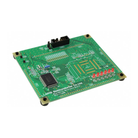
- Page 6 ML610Q102 Reference Board User’s Manual 1.2 The external view of a board The external view of ML610Q174 ReferenceBoard is shown. CNUE UVDD XT_2 XT_1 OSC_2 OSC_1 VREF Socket Mounting P90-P91 P20-P23 Fig.1. ML610Q174 ReferenceBoard External view 1pin Fig.2. Direction of device set When a device is set to a reference board, please carry out, where the power is turned off.
- Page 7 ML610Q174 Reference Board User’s Manual 2. Function 2.1 PWR Jumper It is a jumper which selects the power source of this board. When supplying voltage from uEASE, set a PWR jumper to the "uE" side. The ability to supply power of the uEASE is +3.3v/100mA.
- Page 8 ML610Q102 Reference Board User’s Manual 2.2 The case of using successive approximation ADC When a conversion target is inputted into AIN0-AIN11, without going via CN1/CN4, Please cut the pattern of AIN0-AIN11 if needed and input from the hole near a device. The example of processing is shown below.
- Page 9 ML610Q174 Reference Board User’s Manual 2.3 The case of using light emitting diodes P20-P23, P90-P91 can drive direct to light emitting diodes. P20-P23, P90-P91 are wired with light emitting diodes on this board. Please remove the parts mounted in SP1-SP6.
- Page 10 ML610Q102 Reference Board User’s Manual 2.5 P10-P11 is used as general purpose input ports P10-P11 can change and use a 8MHz oscillation terminal and a general input port terminal. When you use it as a general input port terminal, please remove an 8MHz oscillator and short-circuit SP9/SP10 and SP13/SP14, respectively.
-
Page 11: User Interface
ML610Q174 Reference Board User’s Manual User interface 3.1 The user interface of ML610Q174 Reference Board The pin assignment of CN1, CN2, CN3 and CN4 of the reference board embedded ML610Q174 in below is shown. Table 1. ML610Q174 Reference Board CN1 / CN2 Name Name Pin No. - Page 12 ML610Q102 Reference Board User’s Manual Table 2. ML610Q174 Reference Board CN3 / CN4 Name Name Pin No. Pin No. PD4/SEG20 P20/LED0/LSCLK/PWM4 PD5/SEG21 P21/LED1/OUTCLK/PWM5 PD6/SEG22 P22/LED2/TM9OUT PD7/SEG23 P23/LED3/TMBOUT P90/LED4 P91/LCD5 PF0/SEG32/SIN0 PF1/SEG33/SCK0 PF2/SEG34/RXD0/SOUT0 PF3/SEG35/TXD0/PWM4/TXD1 PF4/SEG36/SIN1/PWM4 PF5/SEG37/SCK1/PWM5 P47/T9BCK/AIN7/CMP1M PF6/SEG38/RXD1/SOUT1/PWM6 P46/T8AP6CK/AIN6/CMP0M PF7/SEG39/TXD1/TXD0 P45/T1P5CK/AIN5...
- Page 13 ML610Q174 Reference Board User’s Manual The circuit diagram and substrate dimensional drawing The circuit diagram and substrate dimensional drawing of this board are shown after a next page.
- Page 14 PIN79 P11/OSC1 PIN79 P11/OSC1 P20/LED0 P20/LED0 PIN80 P10/OSC0 PIN80 P10/OSC0 P21/LED1 P21/LED1 OSC_1 OSC_2 PIN[80:1] 2/1A VREF_IN VREF 2/2A 2/2A LAPIS Semiconductor Co., Ltd. TITLE ML610Q174 Reference Board APPLICATION ML610Q174 DWG NO QTS-11583 DRAWN By SHEET 1 of 2 1.00...
- Page 15 P82/COM2 P02/EXI2 1/2A PIN39 1/1D PIN78 P81/COM1 P03/EXI3 1/2A PIN40 P80/COM0 UVDD CNUE CN14P PIN74 1/1D TEST1_N PIN73 1/1D TEST0 LAPIS Semiconductor Co., Ltd. TITLE ML610Q174 Reference Board APPLICATION ML610Q174 DWG NO QTS-11583 DRAWN By SHEET 2 of 2 1.00...
Need help?
Do you have a question about the ML610Q174 and is the answer not in the manual?
Questions and answers