Table of Contents
Advertisement
Quick Links
Advertisement
Table of Contents

Related Manuals for VMIC VMIVME-7487A

Summary of Contents for VMIC VMIVME-7487A
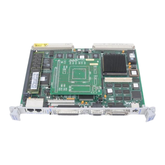
- Page 1 (217) 352-9330 | Click HERE Find the Abaco Systems / VMIC VMIVME-7487-222 at our website:...
- Page 2 VMIVME-7487A 486 PC/AT VMEbus CPU WITH DUAL-PORT MEMORY, PC/104, AND CACHE PRODUCT MANUAL DOCUMENT NO. 500-107487-000 C Revised July 21, 1997 VME MICROSYSTEMS INTERNATIONAL CORPORATION 12090 SOUTH MEMORIAL PARKWAY HUNTSVILLE, AL 35803-3308 (205) 880-0444 (800) 322-3616 FAX NO.: (205) 882-0859...
- Page 3 VMIC assumes no responsibility resulting from omissions or errors in this manual, or from the use of information contained herein. VMIC reserves the right to make any changes, without notice, to this or any of VMIC’s products to improve reliability, performance, function, or design.
- Page 4 2. Block transfer master(s) can reassert AS* and execute a BLT 64 Address Broadcast quickly (less than about 100 ns AS* hightime). The VIC64 as used on the VMIVME-7487A does not cause trouble during Master Mode. In other words, the VMIVME-7487A can safely do master BLT 64 transactions under all conditions. The described malfunction only occurs when the VIC64 is a BLT 64 slave (read from/by master) and the slave transaction is rapidly followed by another BLT 64 slave transaction to another slave.
- Page 5 RECORD OF REVISIONS REVISION PAGES INVOLVED DATE CHANGE NUMBER LETTER 01/25/96 Release 96-0110 05/01/96 Cover and Page ii 96-0313 07/21/97 Cover and Page iii 97-0538 REV LTR PAGE NO. VME MICROSYSTEMS INT’L CORP. DOC. NO. 500-107487-000 12090 South Memorial Parkway Huntsville, AL 35803-3308 •...
- Page 6 VMIC SAFETY SUMMARY THE FOLLOWING GENERAL SAFETY PRECAUTIONS MUST BE OBSERVED DURING ALL PHASES OF THE OPERATION, SERVICE, AND REPAIR OF THIS PRODUCT. FAILURE TO COMPLY WITH THESE PRECAUTIONS OR WITH SPECIFIC WARNINGS ELSEWHERE IN THIS MANUAL VIOLATES SAFETY STANDARDS OF DESIGN, MANUFACTURE, AND INTENDED USE OF THIS PRODUCT. VME...
- Page 7 SAFETY SYMBOLS GENERAL DEFINITIONS OF SAFETY SYMBOLS USED IN THIS MANUAL Instruction manual symbol: the product is marked with this symbol when it is necessary for the user to refer to the instruction manual in order to protect against damage to the system. Indicates dangerous voltage (terminals fed from the interior by voltage exceeding 1000 volts are so marked).
-
Page 8: Table Of Contents
TABLE OF CONTENTS CHAPTER 1 - INTRODUCTION ..........1-1 SECTION 1 - INTRODUCTION TO THE VMIVME-7487A .....1-1 SECTION 2 - ABOUT THIS MANUAL ...........1-2 SECTION 3 - PRODUCT FAMILY ............1-3 SECTION 4 - REFERENCES ..............1-5 SECTION 5 - PC/AT FEATURES ............1-6 SECTION 6 - VMEbus FEATURES ............1-8... - Page 9 SECTION 2 - VMEbus INTERFACE ............4-2 VMEbus Interface Overview .............. 4-2 VMEbus Interface Hardware ............. 4-3 Programming the VMEbus Interface ..........4-6 SECTION 3 - VMEbus MASTER OPERATION ........4-7 Real Mode Access ................4-8 Protected Mode Access ..............4-10 VMIVME-7487A PRODUCT MANUA L...
- Page 10 SECTION 9 - READ-MODIFY-WRITE CYCLES ........4-34 SECTION 10 - BLOCK TRANSFERS ............4-36 DRAM Refresh Considerations ............4-36 Master BLT Operation ...............4-37 Slave BLT Operation .................4-38 SECTION 11 - VME64 FUNCTIONS ............4-39 Master VME64 operation ..............4-39 Slave VME64 operation ..............4-39 VMIVME-7487A PRODUCT MANUAL viii...
- Page 11 Byte Swapping and the VMEbus ..........4-42 VMIVME-7487A Byte Swapping Hardware ......... 4-43 Master/Slave Byte Swapping ............4-45 SECTION 13 - VMIVME-7487A REGISTERS ........4-46 REGISTER MAPS ................4-46 SYSTEM REGISTER DETAILS ............4-52 General Purpose Command Register .......... 4-52 Product ID Register ..............
- Page 12 APPENDIX A - CONNECTOR PINOUTS ........A-1 SECTION 1 - INTRODUCTION ..............A-1 SECTION 2 - ETHERNET CONNECTOR PINOUT .......A-3 SECTION 3 - FLOPPY DRIVE CONNECTOR PINOUT ......A-4 SECTION 4 - IDE HARD DRIVE CONNECTOR PINOUT .....A-5 SECTION 5 - KEYBOARD CONNECTOR PINOUT ......A-6 VMIVME-7487A PRODUCT MANUAL...
- Page 13 SECTION 3 - COPYING FILES TO FLASH MEMORY ......C-3 SECTION 4 - USING FLASH MEMORY AS BOOT DEVICE ....C-4 SECTION 5 - REPROGRAMMING FLASH MEMORY ......C-4 SECTION 6 - TECHNICAL DETAILS ............ C-5 SECTION 7 - PROGRAMMING ............. C-6 VMIVME-7487A PRODUCT MANUA L...
- Page 14 Type .....................D-11 Cylinders ..................D-13 Heads ...................D-13 Sectors/Track ................D-13 Write Precomp ................D-13 MEMORY CACHE SUB-MENU ............D-14 Internal Cache ................D-15 External Cache ................D-15 Cache Shadow Region ..............D-15 Non-Cacheable Region ..............D-15 MEMORY SHADOW SUB-MENU .............D-16 System Shadow ................D-17 Video Shadow ................D-17 VMIVME-7487A PRODUCT MANUAL...
- Page 15 Save Changes & Exit ..............D-23 Discard Changes & Exit ............... D-23 Load Default Values ..............D-23 Load Previous Values ..............D-24 Save Changes ................D-24 SECTION 7 - STATUS AND ERROR MESSAGES ....... D-24 xiii VMIVME-7487A PRODUCT MANUA L...
- Page 16 LIST OF FIGURES Figure 1-1 VMIVME-7487A Board View ..........1-3 Figure 1-2 VMIVME-7487A Partial Block Diagram ......1-7 Figure 1-3 VMIVME-7487A VMEbus Functions .......1-9 Figure 2-1 I/O Port and Jumper Locations ........2-3 Figure 2-2 LED Position on the Front Panel ........2-5 Figure 2-3 PC/104 Mechanical Connection ........2-7...
- Page 17 LIST OF FIGURES 500-107487-000 Figure A-1 VMIVME-7487A Connector Locations ......A-2 Figure A-2 Ethernet Connector Pinout ..........A-3 Figure A-3 Floppy Drive Connector Pinout ........A-4 Figure A-4 IDE Hard Drive Connector Pinout ........A-5 Figure A-5 PS/2 Keyboard Connector Pinout ......... A-6 Figure A-6 PC/AT Keyboard Connector Pinout ......
- Page 18 500-107487-000 LIST OF FIGURES Figure D-9 PhoenixBIOS Keyboard Features Sub-menu ....D-21 Figure D-10 PhoenixBIOS Exit Menu ..........D-23 VMIVME-7487A PRODUCT MANUAL...
- Page 19 LIST OF TABLES Table 1-1 PC/AT I/O Features ............1-8 Table 2-1 VMIVME-7487A Jumper Functions and Settings ..2-4 Table 2-2 VMEbus Window Addresses ..........2-9 Table 3-1 VMIVME-7487A Memory Map .........3-3 Table 3-2 VMIVME-7487A I/O Address Map ........3-5 Table 3-3 PC/AT Hardware Interrupts ..........3-8 Table 3-4 PC/AT Interrupt Vector Table .........3-9...
- Page 20 500-107487-000 LIST OF TABLES Table D-2 PhoenixBIOS Fixed Disk Table ........D-12 Table D-3 PhoenixBIOS Status and Error Messages ....D-25 VMIVME-7487A PRODUCT MANUAL xviii...
-
Page 21: Chapter 1 - Introduction
PC/AT compatible operating system. Its keyboard and video console interaction with the user is typical of a PC/AT. This PC/AT mode of the VMIVME-7487A is discussed in Chapter 3 of this manual. After booting, the VMIVME-7487A may take on the additional functions of a VMEbus controller and interact with other VMEbus modules. -
Page 22: Section 2 - About This Manual
Note that there are many possible segment:offset addresses for a single location. The formula above will provide a unique segment:offset address by forcing the segment to an even 64 Kbyte boundary, e.g., $C000, $E000, etc. When using this formula, make sure to round the offset calculation properly! VMIVME-7487A PRODUCT MANUAL... -
Page 23: Section 3 - Product Family
500-107487-000 PRODUCT FAMILY SECTION 3 - PRODUCT FAMILY Figure 1-1 shows a simpliÞed view of the VMIVME-7487A board. The VMIVME-7487A is one member of VMIC's line of PC/AT compatible VMEbus controllers, all of which combine a standard PC/AT architecture with the ability to control VMEbus slave boards. - Page 24 VMEbus interface. VMIC also has other support products for the PC/AT compatible VMEbus controller line. The VMIVME-7450 is a dual-slot module which holds one 3.5 inch ßoppy drive and one 3.5 inch hard drive. The VMIVME-7451 is a single slot module which holds one 3.5 inch ßoppy drive and up to two...
-
Page 25: Section 4 - References
There are many books widely available on the subject of general PC/AT use and programming. Some reference sources which may be particularly helpful in using or programming the VMIVME-7487A are listed below. i486 Microprocessor Programmer's Reference Manual and the Intel 486DX Microprocessor Data Book Intel Corporation Literature Sales Dept. -
Page 26: Section 5 - Pc/At Features
CHAPTER 1 - INTRODUCTION 500-107487-000 SECTION 5 - PC/AT FEATURES The VMIVME-7487A performs all the functions of a standard IBM PC/AT motherboard with the following features: ¥ Single-Slot 6U Size ¥ High-performance 80486 processor Available with either a DX2/66 or a DX4/100 processor... -
Page 27: Figure 1-2 Vmivme-7487A Partial Block Diagram
500-107487-000 PC/AT FEATURES Figure 1-2 VMIVME-7487A Partial Block Diagram VMIVME-7487A PRODUCT MANUAL... -
Page 28: Section 6 - Vmebus Features
LED Indicators Front Panel Hard Drive Activity SECTION 6 - VMEbus FEATURES In addition to its PC/AT functions, the VMIVME-7487A has the following VMEbus features: ¥ Single-slot, 6U height VMEbus board ¥ Complete 6-line Address ModiÞer (AM-Code) programmability ¥ 32-bit data interface with separate hardware byte/word swapping for master and slave accesses ¥... - Page 29 DTB Arbitration Priori ty Interrupt Util ity Figure 1-3 VMIVME-7487A VMEbus Functions Figure 1-3 shows the VMIVME-7487A functions in a typical VMEbus system. The VMIVME-7487A is a versatile single-board solution for VMEbus control with familiar PC/AT operation. VMIVME-7487A PRODUCT MANUAL...
- Page 30 CHAPTER 1 - INTRODUCTION 500-107487-000 1-10 VMIVME-7487A PRODUCT MANUAL...
- Page 31 SECTION 7 - PC/104 EXPANSION SITE SECTION 8 - BIOS SETUP SECTION 9 - CONFIGURING OPERATING SYSTEMS SECTION 1 - INTRODUCTION This chapter describes unpacking, inspection, hardware jumper settings, connector deÞnitions, installation, system setup, and operation of the VMIVME-7487A. VMIVME-7487A PRODUCT MANUAL...
-
Page 32: Chapter 2 - Installation And Setup
All claims arising from shipping damage should be Þled with the carrier and a complete report sent to VMIC together with a request for advice concerning the disposition of the damaged item(s). -
Page 33: Section 3 - Hardware Setup
500-107487-000 HARDWARE SETUP SECTION 3 - HARDWARE SETUP The VMIVME-7487A has been tested for system operation and shipped with factory-installed header jumpers. Figure 2-1 illustrates the physical location of the user-conÞgurable jumpers and connectors on the board. Table 2-1 on page 2-4 lists each jumper designator, its function, and the factory-installed default conÞguration. - Page 34 * Note that the Alternate LPT1 address at I/O $3BC cannot be configured as an EPP port. NOTE: ANY OTHER JUMPER LOCATIONS ARE RESERVED FOR VMIC USE ONLY AND SHOULD NOT BE ALTERED FROM THE FACTORY DEFAULT SETTINGS. VMIVME-7487A PRODUCT MANUAL...
-
Page 35: Section 4 - Led Status Definition
* * * * * * * * * * DO NOT INSTALL OR REMOVE BOARD WHILE POWER IS APPLIED. The VMIVME-7487A conforms to the VMEbus physical speciÞcation for a 6U x 4HP dual Eurocard (dual height, single-slot width). It can be plugged directly into any standard chassis accepting this type of board. -
Page 36: Section 6 - Front Panel Connectors
CHAPTER 2 - INSTALLATION AND SETUP 500-107487-000 3. Choose a chassis slot. The VMIVME-7487A may be attached to a dual P1/P2 VMEbus backplane or a single P1 backplane. A single P1 connection supplies enough power and allows 16-bit data transfers and 24-bit addressing, but for 32-bit data transfers and 32-bit addressing a dual P1/P2 backplane is required. -
Page 37: Section 7 - Pc/104 Expansion Site
500-107487-000 PC/104 EXPANSION SITE a keyboard with a standard PC/AT connector to the VMIVME-7487A. See Appendix A for connector pinouts and orientation. SECTION 7 - PC/104 EXPANSION SITE Expansion boards that are PC/104 compatible install directly to the VMIVME-7487AÕs PC/104 Expansion Site (see Figure 2-1 on page 2-3). -
Page 38: Section 8 - Bios Setup
The VMIVME-7487A is shipped from the factory with no hard or ßoppy drives conÞgured in CMOS. The BIOS Setup program must be run to conÞgure the speciÞc drives attached. It is recommended that the user follow the procedure for Quick BIOS Setup in Appendix D to properly conÞgure the system. -
Page 39: Configuration Examples
VMEbus Window is translated into a VMEbus access once VMEbus access is enabled. The complete VMIVME-7487A memory map is presented in Chapter 3, but for reference the address ranges to be excluded for the VMEbus Windows are listed in Table 2-2. -
Page 40: Configuring Windows For The Vmivme-7487A
Configuring Windows for the VMIVME-7487A Microsoft Windows will run well on the VMIVME-7487A, but the Real Mode VMEbus Window needs to be excluded from its memory manager. Edit the SYSTEM.INI Þle in the main Windows directory and add the... -
Page 41: Chapter 3 - Pc/At Functions
Base Index Sequencer Burst Prefetcher 32-bit Displacement Bus Control Cache 32-byte Control Code Queue MicroInstruction Bus (2x16 bytes) Control and Protection Instruction Unit Decoded Decode Instructions 24-bit Register Control Code File Stream Figure 3-1 80486 CPU Block Diagram VMIVME-7487A PRODUCT MANUAL... -
Page 42: Section 2 - Physical Memory
The VMIVME-7487A includes both the system and video BIOS in a single 128 K x 8 EPROM. The system portion of this ROM (at $F0000) is automatically shadowed, but for higher performance it is recommended that shadow RAM for the video BIOS be enabled (see Appendix D). -
Page 43: Section 3 - Memory And Port Maps
SECTION 3 - MEMORY AND PORT MAPS MEMORY MAP The memory map for the VMIVME-7487A is shown in Table 3-1. All systems share this same memory map, although a VMIVME-7487A with less than the full 32 Mbytes of DRAM does not Þll the entire space reserved for On-Board Extended Memory. -
Page 44: I/O Port Map
This limits the PC/104 address space to 1024 locations ($000-$3FF). The VMIVME-7487A incorporates all standard I/O peripherals of the PC/AT architecture such as keyboard, DMA, interrupt controllers, timers and real-time clock, as well as parallel and serial I/O ports, video registers, and ßoppy and hard drive task registers. -
Page 45: Table 3-2 Vmivme-7487A I/O Address Map
500-107487-000 MEMORY AND PORT MAPS Table 3-2 VMIVME-7487A I/O Address Map SIZE IN ASSOCIATED ADDRESS HARDWARE DEVICE PC/AT FUNCTION † BYTES JUMPERS RANGE DMA Controller 1 $000 - $00F ACC Micro 2168 Chip (Intel 8237A Compatible) $010 - $01F Reserved... - Page 46 CHAPTER 3 - PC/AT FUNCTIONS 500-107487-000 Table 3-2 VMIVME-7487A I/O Address Map (Continued) SIZE IN ASSOCIATED ADDRESS HARDWARE DEVICE PC/AT FUNCTION † BYTES JUMPERS RANGE VMEbus Interface Registers $140 - $14F Custom VMIC Hardware E16 & E11 (see Chapter 4 for details)
- Page 47 $46E9 - $FFFF 47383 Reserved * While these I/O ports are reserved for the listed functions, they are not implemented on the VMIVME-7487A. They are listed here to make the user aware of the standard PC/AT usage of these ports. †...
-
Page 48: Section 4 - Pc/At Interrupts
Table 3-4 on page 3-9 details the vectors in the interrupt vector table. Table 3-3 PC/AT Hardware Interrupts AT FUNCTION COMMENTS Parity Errors Used by VMIVME-7487A VMEbus (Must be enabled in BIOS Setup) Interface System Clock/Calendar Set by BIOS Setup System Clock/Calendar Set by BIOS Setup... -
Page 49: Table 3-4 Pc/At Interrupt Vector Table
Same as Real Mode BIOS Keyboard I/O Same as Real Mode BIOS Printer I/O Same as Real Mode ROM BASIC Entry Point Same as Real Mode Bootstrap Loader Same as Real Mode IRQ8 Real-Time Clock Same as Real Mode VMIVME-7487A PRODUCT MANUAL... - Page 50 DOS Print Spooler Driver Same as Real Mode 30-60 48-96 Reserved by DOS Same as Real Mode 61-66 97-102 User Available Same as Real Mode 68-71 103-113 Reserved by DOS Same as Real Mode IRQ10 Same as Real Mode 3-10 VMIVME-7487A PRODUCT MANUAL...
- Page 51 IRQx line. The interrupt hardware implementation on the VMIVME-7487A is standard for computers built around the PC/AT architecture, which evolved from the IBM PC/XT. In the IBM PC/XT computers only eight interrupt request lines exist, numbered from IRQ0 to IRQ7 at the PIC.
-
Page 52: Section 5 - Enhanced I/O Ports
CHAPTER 3 - PC/AT FUNCTIONS 500-107487-000 Figure 3-2 depicts the VMIVME-7487A interrupt logic pertaining to VMEbus operations. Note that the NMI interrupt generated by the VMIVME-7487A must be enabled in the BIOS Setup (see Appendix D). 8259 MASTER-PORTS $020-$021 IRQ1* IRQ2*... -
Page 53: Serial Ports
Windows communications port drivers that address this problem. PARALLEL PORT The VMIVME-7487AÕs enhanced parallel port may be conÞgured for any one of four modes as deÞned by IEEE Standard 1284 shown in Table 3-5. Table 3-5... -
Page 54: Section 6 - Video Graphics Adapter
SECTION 6 - VIDEO GRAPHICS ADAPTER The monitor port on the VMIVME-7487A is controlled by a Cirrus Logic chip with 1 Mbyte video DRAM. The video controller chip is hardware and BIOS compatible with the IBM EGA and VGA standards and also supports VESA high-resolution and extended video modes. -
Page 55: Section 7 - Pc/104 Expansion Site
I/O functions. VMICÕs VMIVME-7432 PC/104 to ISA Adapter is designed speciÞcally to mate with the VMIVME-7487A, allowing it to use a standard half-length ISA bus board in the same chassis. This expansion allows low-cost or specialty ISA bus boards to be used in the same chassis with VMEbus equipment. - Page 56 CHAPTER 3 - PC/AT FUNCTIONS 500-107487-000 3-16 VMIVME-7487A PRODUCT MANUAL...
-
Page 57: Chapter 4 - Vmebus Functions
The register details are provided last for easy reference for the programmer familiar with the VMIVME-7487A, but the novice will need to study the reference section as well. The Þrst-time VMIVME-7487A user is strongly urged to read through the functional sections with a copy of the register and bit maps (beginning on page 4-47) close at hand. -
Page 58: Section 2 - Vmebus Interface
VMIVME-7487A and the VMEbus. Note that the VMEbus is connected to the 80486 local bus. In Real Mode, the VMIVME-7487A uses a paging scheme to access any part of the 4 Gbytes of VMEbus addressing space 64 Kbytes at a time through the Real Mode VMEbus Window at $E0000. -
Page 59: Vmebus Interface Hardware
U t il i t y Figure 4-1 VMIVME-7487A VMEbus Functions In Protected Mode, the VMIVME-7487A can access the VMEbus through the Protected Mode VMEbus Window, which occupies 1024 Mbytes beginning at $4300 0000. This 1024 Mbyte space is divided into 16 equal spaces of 16 Mbytes, each corresponding to the VMEbus but with different VMEbus Address ModiÞers. - Page 60 The CPU interface of the VIC was designed to be part of a Motorola 68030 system. An interface is required to connect the 80486 bus to the 68030-like CPU interface of the VIC. This connection is accomplished by the VLIC as shown in Figure 4-3 on page 4-5. VMIVME-7487A PRODUCT MANUAL...
- Page 61 DRAM is requested. The 2168 requests the local bus when a DRAM refresh is required or when the 2168 DMA controller needs the bus. The data multiplexer function is used to implement byte swapping. Byte swapping is implemented in both directions (both VMIVME-7487A acting VMIVME-7487A PRODUCT MANUAL...
-
Page 62: Programming The Vmebus Interface
CHAPTER 4 - VMEbus FUNCTIONS 500-107487-000 as VMEbus master and VMIVME-7487A being accessed as a VMEbus slave). The VLIC contains system registers that allow the VMIVME-7487A VMEbus interface to be programmed. The VLIC also contains hardware to translate the 68030-like interrupt structure of the VIC to the PC/AT interrupt structure. -
Page 63: Section 3 - Vmebus Master Operation
Interrupt Acknowledge Registers. SECTION 3 - VMEbus MASTER OPERATION The VMIVME-7487A VMEbus interface allows the 80486 to access the VMEbus while in Real Mode or Protected Mode. In Real Mode, the VMIVME-7487A accesses the VMEbus using a paging scheme to address any part of the 4 Gbyte VMEbus through a 64 Kbyte window at $E0000. -
Page 64: Real Mode Access
The upper address bits are contained in the Extended/Standard Address Register (VMEbus address bits A31-A16). The lower address bits (VMEbus address bits A15-A0) are driven directly by the CPU. See Figure 4-4 on page 4-9 for a graphic representation of Real Mode VMEbus access. VMIVME-7487A PRODUCT MANUAL... -
Page 65: Figure 4-4 Real Mode Vmebus Access
VMEbus MASTER OPERATION VIC64 REGISTER AMSR REGISTER AM5-AM0 SYSTEM REGISTER EXT_STD_ADDR REGISTER A31-A16 A15-A1 A15-A1 80486 D31-00 D31-D0 80486 = REAL MODE 80486 A19-A16 = 1110 = $E GP_COMMAND VME_EN = 1 Figure 4-4 Real Mode VMEbus Access VMIVME-7487A PRODUCT MANUAL... -
Page 66: Protected Mode Access
The address size and type for each region are shown in Table 4-1 on page 4-11. See Figure 4-5 on page 4-12 for a pictorial representation of Protected Mode access. 4-10 VMIVME-7487A PRODUCT MANUAL... - Page 67 Source Register (AMSR). Shaded fields define the address modifier when the AM2-0 Option bit is set. The bit is clear by default. See page 4-78 for a detailed description of this bit. Note: A25 + A24 MUST=1 VMIVME-7487A PRODUCT MANUAL 4-11...
-
Page 68: Figure 4-5 Protected Mode Vmebus Access
After powerup, accessing VMEbus in Protected Mode requires at least the following steps: 1. Initialize the VIC Base Register. Program the VIC base address and enable access to the VIC by setting the VIC Enable bit. 4-12 VMIVME-7487A PRODUCT MANUAL... -
Page 69: Section 4 - Vmebus Slave Operation
80486 ADDRESS BITS A25-A24 MUST BE SET TO 1 DURING VMEBUS PROTECTED MODE ACCESS. SECTION 4 - VMEbus SLAVE OPERATION The VMIVME-7487A has two resources that are accessible by VMEbus slave accesses: VIC interprocessor communication facilities and dual-port DRAM. INTERPROCESSOR COMMUNICATIONS... - Page 70 Register (ICR7) provides semaphore bits associated with each of the Þve mailbox registers. The other ICR registers allow a VMEbus master to gain status information about the VMIVME-7487A. See page 4-98 for a complete description of all Interprocessor Communications Registers.
-
Page 71: Figure 4-6 Vmebus Slave Interface
As Figure 4-6 shows, the LSB CY7C964 has a MATCH* output which is connected to the VIC ICFSEL* input. The MATCH* signal is activated VMIVME-7487A PRODUCT MANUAL 4-15... - Page 72 Address Compare. VMEbus address bits deÞned in the Slave A16 Address Compare register become ÒdonÕt caresÓ when the corresponding bit in the Slave A16 Address Mask register is programmed with a 1. See Figure 4-7 on page 4-17 for a graphic description of both registers. 4-16 VMIVME-7487A PRODUCT MANUAL...
-
Page 73: Figure 4-7 Slave Compare Operation
Example: Program VIC ICR registers to reside at VMEbus address $A500 1. Write 0xA500 data to Slave A16 Address Compare register. 2. Write 0x0 to Slave A16 Address Mask register. 3. Set Mailbox Enable bit in General Purpose Command system register. VMIVME-7487A PRODUCT MANUAL 4-17... -
Page 74: Dual-Ported Dram
4. Initialize the General Purpose Command Register. Other bits may be set depending on the application. DUAL-PORTED DRAM All of the VMIVME-7487AÕs DRAM (1 Mbyte - 16 Mbytes, depending on memory option ordered) is accessible from the VMEbus. More accurately, all VMIVME-7487A physical memory is accessible from the VMEbus. - Page 75 Kbytes of RAM has some utility, extreme caution should be used when accessing this region to prevent overwriting the operating system. The VMIVME-7487A slave interface allows the dual-port DRAM slave address to be programmed in software. In addition, the VMEbus can access the DRAM using either A32 Extended addressing or A24 Standard addressing.
- Page 76 Slave A32/A24 Address Compare register become ÒdonÕt caresÓ when the corresponding bit in the Slave A32/A24 Address Mask register are set. Example: Program the VMIVME-7487A slave interface to map 16 Mbytes of on-board DRAM to A32 VMEbus address $1200 0000.
-
Page 77: Slave Access Memory Map
VMEbus slave accesses. The VMIVME-7487A local addresses which map to the VMEbus cannot be accessed since they are off-board resources and would require the VMIVME-7487A to be both VMEbus master and VMEbus slave simultaneously. Table 4-2 on page 4-22 describes accessible and nonaccessible memory regions. -
Page 78: Table 4-2 Slave Access Memory Map
VGA display DRAM $00000 - $9FFFF 640 Kbytes of DRAM * This region of the VMIVME-7487A local address space cannot be accessed from the VMEbus. A31-A25 of the VMIVME-7487A local address bus are forced to 0 when a VMEbus slave access occurs. -
Page 79: System Considerations
VMEbus). During a VMIVME-7487A slave access, VMEbus address bits connect to the VMIVME-7487A local address bits as shown in Figure 4-8. Note that local address bits A31-A25 are always driven to 0 during a slave access. VMIVME-7487A PRODUCT MANUAL... -
Page 80: Figure 4-8 Slave Addressing Detail
A31 - A25 N. C. CY7C964 A31 - A24 A23 - A16 CY7C964 A23 - A16 A15 - A8 CY7C964 A15 - A8 A7 - A0 A7 - A1 VIC64 DS0* DS1* Figure 4-8 Slave Addressing Detail 4-24 VMIVME-7487A PRODUCT MANUAL... -
Page 81: Section 5 - System Controller Functions
The VMIVME-7487A has a hardware bus timeout circuit that is independent of the VIC. This function is provided since the bus timeout in the VIC can only be enabled when the VMIVME-7487A is the system controller. In addition, the hardware timer offers a timeout value (1 0 µ s) that is not offered by the VIC. -
Page 82: Section 6 - Vmebus Interrupt Handling
VMIVME-7487A operation is 1 0 µ s. This value is dictated by the DRAM refresh time for the VMIVME-7487AÕs memory. Timeouts beyond the 1 0 µ s limit risk memory corruption due to lack of refresh. -
Page 83: Table 4-3 Interrupt Priorities
ID for highest priority pending interrupt that is programmed with that level. The VMIVME-7487A allows the user to choose one of three PC/AT interrupt channels to be used for interfacing with the VIC interrupts: IRQ11, IRQ12, or the NMI. The user programs each source to interrupt the 80486 on one of these PC/AT interrupts by using interrupt levels. -
Page 84: Table 4-4 Interrupt Level Assignments
The VIC to local bus interface (VLIC) relies on getting a DTACK from the VIC for synchronization with the 80486 local bus. Failure to receive a VIC DTACK will lock the 80486 bus. 4-28 VMIVME-7487A PRODUCT MANUAL... - Page 85 The VMIVME-7487A IRQ11 and IRQ12 interrupts are dedicated for use with the VIC and therefore are not shared by any other on-board resource. In contrast, the VMIVME-7487A NMI interrupt is shared by the VIC and other on-board circuitry. The PC/AT architecture deÞnes two possible sources for the NMI: on-board parity errors and off-board parity errors.
-
Page 86: Software Interrupts
ID register within the appropriate interrupt service routine. INTERRUPT ON BERR* The VMIVME-7487A allows the 80486 to receive an interrupt if the VMIVME-7487A causes a VMEbus BERR*. This is particularly important feature given that the 80486 CPU does not directly support bus error conditions. -
Page 87: Interrupt Processing
PC/AT hardware. These operations are shown for the IRQ11 and IRQ12 interrupts in Figure 4-9 on page 4-32. Operation for the NMI interrupt is shown in Figure 4-10 on page 4-33. VMIVME-7487A PRODUCT MANUAL 4-31... -
Page 88: Figure 4-9 Flow Chart For Non-Nmi Interrupt Processing For Irq11
2 interrupt Initialize source vectors in VIC64 Write EOI to 8259 pic Unmask IR11 in 8259 PIC Write REARM_INT Register ISR Ready End ISR Figure 4-9 Flow Chart for Non-NMI Interrupt Processing for IRQ11 4-32 VMIVME-7487A PRODUCT MANUAL... -
Page 89: Section 7 - Vmebus Interrupter
IRQ is acknowledged by an off-board interrupt handler, the VIC supplies the vector associated with that interrupt provided the VMIVME-7487A IACKIN* signal is active. The VMIVME-7487A can be programmed to interrupt the CPU when a VMIVME-7487A issued VMEbus interrupt has been acknowledged. This is VMIVME-7487A PRODUCT MANUAL... -
Page 90: Section 8 - Vmebus Requester
(RMW) cycles to be performed. Slave VMEbus RMW cycles require no special programming of the VMIVME-7487A. The VIC will keep the local bus on behalf of the VMEbus slave access until the read and write portion of the cycle is completed. The 80486 is not allowed to interrupt the local bus read-modify-write cycle. - Page 91 80486 LOCK* bus signal. The 80486 LOCK* signal is connected to the RMC* input of the VIC. When the VIC detects a master VMEbus request by the VMIVME-7487A and the activation of the RMC* input, a VMEbus RMW cycle is performed. Note that this ÒlockedÓ...
-
Page 92: Section 10 - Block Transfers
In addition, a VMIVME-7487A with the VIC64 supports 64-bit block transfers. All BLT modes are described in this section. DRAM REFRESH CONSIDERATIONS During BLTs, the VIC chip becomes a bus master on the VMIVME-7487A local bus. -
Page 93: Master Blt Operation
MASTER BLT OPERATION The VMIVME-7487A performs BLT using the VIC local DMA mode. The ÒMOVEMÓ mode of VIC BLT is not supported on the VMIVME-7487A. The VIC allows local DMA mode to be operated in accelerated mode or single cycle mode. -
Page 94: Slave Blt Operation
As described in Section 4, the slave select 0 VIC input is used for A32 slave accesses and slave select 1 is used for A24 slave accesses. Prior to the slave BLT the VIC slave select registers must be programmed to allow for A32 or 4-38 VMIVME-7487A PRODUCT MANUAL... -
Page 95: Section 11 - Vme64 Functions
SS1CR0 registers. Also, program the corresponding SS0CR1 or SS1CR1 register to 0x0. Program the LBTR to 0xFF. SECTION 11 - VME64 FUNCTIONS A VMIVME-7487A with the VME64 installed may transfer 64 bits at a time using VME64 MBLT block transfers. MASTER VME64 OPERATION As deÞned in Section 13, the BTDR register has additional bit Þelds that the... -
Page 96: Section 12 - Byte Ordering
Double Byte(2-3) Byte(2) Byte(3) Double Byte(0-1) Byte(0) Byte(1) Quad Byte(0-3) Byte(0) Byte(1) Byte(2) Byte(3) It is important to note the major byte ordering differences between the VMEbus and the Intel 80486 CPU. In addition, communication between 4-40 VMIVME-7487A PRODUCT MANUAL... -
Page 97: The Byte Swapping Problem Defined
Òlittle-endianÓ ordering. The VMIVME-7487A uses an Intel 80486 microprocessor, which uses little-endian byte ordering. Byte arrangement and the byte relationship between data in the processor and transferred data in memory are shown in Figure 4-11. -
Page 98: Byte Swapping And The Vmebus
Table 4-5 on page 4-40, byte(0) must be transferred on data lines D31-D24 during a longword transfer while byte(3) must be transferred on lines D7-D0. This byte and address alignment is exactly the same as that for 4-42 VMIVME-7487A PRODUCT MANUAL... -
Page 99: Vmivme-7487A Byte Swapping Hardware
VMEbus with its byte lanes crossed. For example, the 80486 uses D0-D7 to transfer a byte to address $00, while the VMEbus requires D8-D15 be used. For this reason, special hardware has been incorporated into the VMIVME-7487A to facilitate different kinds of byte swapping for varying circumstances. VMIVME-7487A Byte Swapping Hardware... -
Page 100: Figure 4-13 80486-To-Vmebus Data Byte Lanes
Table 4-6 details this relationship. Table 4-6 Byte Swap Modes BIG ENDIAN SIZE OF TRANSFER SWAP MODE BIT STATUS single byte byte-swap word (two bytes) byte-swap longword (four bytes) word-swap word (two bytes) direct longword (four bytes) direct 4-44 VMIVME-7487A PRODUCT MANUAL... -
Page 101: Master/Slave Byte Swapping
On the VMIVME-7487A, byte ordering can be programmed for either big-endian or little-endian in both directions (that is, whether the VMIVME-7487A is a VMEbus master or a VMEbus slave). Two bits in the General Purpose Command Register control the byte-ordering modes for master and slave accesses: Master Big Endian, and Slave Big Endian. - Page 102 The VMIVME-7487A has three groups of custom registers: ¥ System Registers (9) ¥ Interrupt Acknowledge Registers (3) ¥ VIC Registers (58) All registers are in I/O addressing space, but only the System Registers have a Þxed location: I/O $140 through I/O $14F. The location of the Interrupt Acknowledge and VIC Registers are determined by the value in the VIC Base Register, a System Register at the Þxed address of I/O $141.
- Page 103 Table 4-7 System Register Map REGISTER NAME PAGE MNEMONIC ACCESS D15 D14 D13 D12 D11 D10 D9 Master Slave Slave Slave General Purpose Status Mailbox 4-52 GP_COMMAND Byte Write $140 Word Enable Enable Command Endian Endian Enable Enable Enable 4-55 Product ID BRD_ID Byte Read...
-
Page 104: Table 4-8 Vic Register Map
ICMS Interrupt Vector Base 4-67 ICMSVBR $453 Status/ID Value Number 4-68 Local Interrupt Vector Base LIVBR $457 Status/ID Value Local Interrupt Number Error Group Interrupt Vector Base 4-68 EGIVBR $45B Status/ID Value G roup Interrupt Number 4-48 VMIVME-7487A PRODUCT MANUAL... -
Page 105: Section 13 - Vmivme-7487A Registers
Minimum PAS Deasserted Time Minimu m PAS Asser ted T i m e asserted Time Accel. Boundary Dual- AMSR 4-74 BTDR $4AB Boundary Slave Block Master Crossing Block Transfer DeÞnition Path Enable Crossing Enable Transfer Enable Enable Enable VMIVME-7487A PRODUCT MANUAL 4-49... - Page 106 The VIC occupies 256 bytes of I/O addressing space from its base at offset $00 to offset $FF: all addresses within that space not assigned to a register are considered Reserved and should not be accessed. Shaded registers are unique because they are available to other VMEbus masters in slave access mode. 4-50 VMIVME-7487A PRODUCT MANUAL...
-
Page 107: Table 4-9 Slave Access Register Map
Set/Clear ICGS registers, which may only be accessed as privileged. The VIC slave-addressable registers occupy 256 bytes of Short I/O addressing space: all addresses within that space not assigned to a register are considered Reserved and should not be accessed. VMIVME-7487A PRODUCT MANUAL 4-51... -
Page 108: System Register Details
The 80486 processor uses IntelÕs little-endian method for transferring a multiple-byte group between its internal registers and external memory. The VMEbus, however, expects MotorolaÕs big-endian method for transferring a multiple-byte group to the same locations. The VMIVME-7487A has hardware on-board to support either transfer 4-52 VMIVME-7487A PRODUCT MANUAL... - Page 109 See the discussion on byte swapping in Section 12 for more details. General Purpose Command Register: Slave A32/A24 Enable bits (D4, D0) Bits 4 and 0 control slave access to the VMIVME-7487A. The default clear state disables all slave accesses to the VMIVME-7487A.
- Page 110 General Purpose Command Register: VME Enable bit (D1) Bit 1 controls master VMEbus access. While this bit is clear Ð the default state after powerup or reset Ð the VMIVME-7487A cannot access the VMEbus as a master. While VMEbus access is disabled, the...
-
Page 111: Product Id Register
VMEbus SYSRESET* when the front panel reset button is pressed, as long as the VMIVME-7487A is conÞgured as the system controller. Likewise, if the VMIVME-7487A is not the system controller, it will still respond to a VMEbus SYSRESET* regardless of the VME Enable bit status. - Page 112 VIC Base Register: LPT Mode bit (D1) This utility bit controls whether or not the VMIVME-7487AÕs parallel port is bidirectional or output only. A clear LPT Mode bit (the default) makes the port bidirectional. A set bit forces the port into an output-only conÞguration.
-
Page 113: Extended/Standard Address Register
Slave Address Mask/Compare Registers These four related write-only word registers are associated with slave mode access to the VMIVME-7487A. See the discussion regarding these registers and slave mode on page 4-13. Programming these registers and then setting the Mailbox Enable bit in the General Purpose Command... -
Page 114: Interrupt Acknowledge Register Details
See the description of the VIC Base Register on page 4-55 for details regarding moving the VIC registers around in I/O addressing space. For complete VIC information, the programmer is strongly urged to acquire the VIC64 UserÕs Guide from Cypress Semiconductor (see 4-58 VMIVME-7487A PRODUCT MANUAL... -
Page 115: Vmebus Interrupter Interrupt Control Register
¥ The register and bit deÞnitions in this manual are customized for this controller; therefore, some more general functions described in the VIC manual either do not apply to the VMIVME-7487A or have slightly different applications. Such differences are pointed out in this manual wherever possible. -
Page 116: Vmebus Interrupt Control Registers
VMEbus Interrupt Control Registers: IPL Value bit field (D2-D0) This interrupt level value is inverted and driven onto the IPL lines when an interrupt is acknowledged. The VMIVME-7487A supports PC/AT NMI interrupts on level 4, and IRQ11 and IRQ12 interrupts on IPL levels 2 and 1, respectively. -
Page 117: Dma Status Interrupt Control Register
The VIC will not issue a local interrupt at the completion of a local VIC DMA operation (default) DMA Status Interrupt Control Register: IPL Value bit field (D2-D0) This value is inverted and driven onto the IPL lines when an interrupt is acknowledged. VMIVME-7487A PRODUCT MANUAL 4-61... -
Page 118: Local Interrupt Control Registers
Do not enable the interrupt until the interrupt handling routines are in place. Also, note that LIRC5 is reserved by VMIC and should never be altered from the default setting. Local Interrupt Control Registers LICR1-7 (VIC offset I/O $427-$43F) -
Page 119: Icgs Interrupt Control Register
Autovector mode required normal VMIVME-7487A operation. When clear, autovector mode is disabled; the interrupting source must provide the Status/ID vector to the processor. Autovector Bit Function The interrupting source provides the status/ID vector for the local interrupt acknowledge cycle to the processor (default) (not supported on the VMIVME-7487A) Autovector mode. -
Page 120: Icms Interrupt Control Register
IPL encoding for the four module switch interrupts. This register is initialized to a value of $F8 upon powerup or hard reset. ICMS Interrupt Control Register ICMSICR (VIC offset I/O $447) ICMS3 ICMS2 ICMS1 ICMS0 Mask Mask Mask Mask Value Value Value 4-64 VMIVME-7487A PRODUCT MANUAL... -
Page 121: Error Group Interrupt Control Register
When this bit is clear, the VIC generates a local interrupt when ACFAIL* is detected as asserted. ACFAIL Mask Bit Function The VIC generates a local interrupt when ACFAIL* is detected as asserted The VIC will not generate a local interrupt when ACFAIL* is detected as asserted (default) VMIVME-7487A PRODUCT MANUAL 4-65... -
Page 122: Icgs Interrupt Vector Base Register
CHAPTER 4 - VMEbus FUNCTIONS 500-107487-000 Error Group Interrupt Control Register: Write Post Fail Interrupt Mask bit (D6) Write posting is not supported on the VMIVME-7487A, therefore bit 6 should remain set. Error Group Interrupt Control Register: Arbitration Timeout Interrupt Mask bit (D5) When this bit is clear, the VIC generates a local interrupt when an arbitration timeout has occurred. -
Page 123: Icms Interrupt Vector Base Register
Bit 2 Bit 1 Bit 0 Number Number ICMS Interrupt Vector Base Register: Status/ID bit field (D7-D2) These bits are user-deÞnable and are used with bits 1-0 to provide a unique module switch interrupt status/ID vector. VMIVME-7487A PRODUCT MANUAL 4-67... -
Page 124: Local Interrupt Vector Base Register
VIC offset I/O address $45B. This register provides the status/ID vector for the error group interrupts. The status/ID must be programmed with a unique number for each VIC interrupt controller in the chassis to enable identiÞcation encoding for bits 2-0. 4-68 VMIVME-7487A PRODUCT MANUAL... -
Page 125: Interprocessor Communications Registers
Please refer to the Interprocessor Communications Registers detailed beginning on page 4-96. VMEbus Interrupt Request/Status Register The VMEbus Interrupt Request/Status Register (VIRSR) is a read/write byte register at VIC offset I/O address $483. This register provides status VMIVME-7487A PRODUCT MANUAL 4-69... -
Page 126: Vmebus Interrupt Vector Base Registers
IRQ3 $493 IRQ4 $497 IRQ5 $49B IRQ6 $49F IRQ7 Transfer Timeout Register The Transfer Timeout Register (TTR) is a read/write byte register at VIC offset I/O address $4A3. This register provides control of the local and 4-70 VMIVME-7487A PRODUCT MANUAL... - Page 127 DeÞnes the VMEbus timeout. Note that the hardware timer, if enabled, will override all settings here except the 4 µs value. See the discussion concerning the system controller functions on page 4-7. VMEbus Timeout (µs) 64 (default) Infinite (timer disabled) VMIVME-7487A PRODUCT MANUAL 4-71...
- Page 128 When clear, the local bus timer will stop and reset when the VMEbus is requested. Include VMEbus Acquisition Bit Function The local bus timer will stop and reset when the VMEbus is requested (default) The local bus timer will include waiting for VMEbus acquisition 4-72 VMIVME-7487A PRODUCT MANUAL...
-
Page 129: Local Bus Timing Register
RMW cycles or BLT transfers on the VMIVME-7487A. Minimum DS Deasserted Time Bit Function The minimum deasserted time for the DS* signal is 15.625 ns (default) The minimum deasserted time for the DS* signal is 31.250 ns VMIVME-7487A PRODUCT MANUAL 4-73... -
Page 130: Block Transfer Definition Register
VMEbus acknowledge timing. This value must be set to maximum (all bits set) when performing slave RMW cycles or BLT transfers on the VMIVME-7487A. Block Transfer Definition Register The Block Transfer DeÞnition Register (BTDR) is a read/write byte register at VIC offset I/O address $4AB. -
Page 131: Interface Configuration Register
When set, the VIC issues the address modiÞer code from the Address ModiÞer Source Register (AMSR) during block transfers. This bit must be set to enable BLT transfers on the VMIVME-7487A. Block Transfer Definition Register: Dual Path Enable bit (D0) When set, dual path mode is enabled on the VIC during master block transfers. - Page 132 If bit 4 is enabled, bit 3 may be used to prevent the assertion of HALT* for RMC deadlocks. The default condition, using the DEDLK* signal alone, is recommended for the VMIVME-7487A and is the only condition possible for slave accesses.
-
Page 133: Arbiter/Requester Configuration Register
The VIC performs round-robin VMEbus arbitration (default) The VIC performs priority VMEbus arbitration Arbiter/Requester Configuration Register: VMEbus Request Level bit field (D6-D5) The VMEbus request level is set according to the following table: VMEbus Request Level BR3 (default) VMIVME-7487A PRODUCT MANUAL 4-77... -
Page 134: Address Modifier Source Register
The VIC performs no DRAM refresh functions (default) The VIC performs CAS-before-RAS (DS* before PAS*) refresh functions. This bit should never be set on the VMIVME-7487A. Arbiter/Requester Configuration Register: Fairness Timer Enable bit field (D3-D0) The VMEbus fair requester is enabled in this bit Þeld according to the... -
Page 135: Bus Error Status Register
VMEbus mastership, and timeout status. All bits except bit 7 are ßags that are automatically cleared on reset and must otherwise be cleared manually by the local processor after being set by status conditions. If these bits are VMIVME-7487A PRODUCT MANUAL 4-79... -
Page 136: Dma Status Register
(LBERR asserted to the VIC). Once set, this bit must be cleared manually. (Local bus Error errors will never occur in the current VMIVME-7487A configuration.) This bit is set when a VMEbus bus error is signaled (BERR asserted). Once set, this... - Page 137 DMA Status Register: Master Write Post Info bit (D7) This bit is set whenever master write post information is stored. Since write posting is not supported on the VMIVME-7487A, this bit should always be clear. DMA Status Register: VMEbus Bus Error bit (D4) This bit is set when a VMEbus bus error is signaled (BERR* asserted).
-
Page 138: Slave Select 0 Control Register 0
VIC offset I/O address $4C3. This register provides control of the slave selection 0 facilities of the VIC, which is dedicated to A32 access only on the VMIVME-7487A. Enabling of the IRQ2 timer interrupt is also conÞgured in this register. This register is initialized to a value of $00 upon powerup or hard reset. - Page 139 DMA. The DSACKi* signals should be held asserted in this mode. This method must be used for block transfers on the VMIVME-7487A. Reserved. When performing BLT transfers, bit 1 must always be set and bit 0 must be clear (for accelerated local bus transfers).
- Page 140 Slave Select 0 Control Register 1 SS0CR1 (VIC offset I/O $4C7) Timing Timing Timing Timing Timing Timing Timing Timing Field 1 Field 1 Field 1 Field 1 Field 0 Field 0 Field 0 Field 0 4-84 VMIVME-7487A PRODUCT MANUAL...
-
Page 141: Slave Select 0 Control Register 1
Timing Delay 0 ns (default) 31.2500 ns 39.0625 ns 46.8750 ns 54.6875 ns 62.5000 ns 70.3125 ns 78.1250 ns 85.9375 ns 93.7500 ns 101.5625 ns 109.3750 ns 117.1875 ns 125.0000 ns 132.8125 ns 140.6250 ns VMIVME-7487A PRODUCT MANUAL 4-85... - Page 142 Timing Delay 0 ns (default) 31.2500 ns 39.0625 ns 46.8750 ns 54.6875 ns 62.5000 ns 70.3125 ns 78.1250 ns 85.9375 ns 93.7500 ns 101.5625 ns 109.3750 ns 117.1875 ns 125.0000 ns 132.8125 ns 140.6250 ns 4-86 VMIVME-7487A PRODUCT MANUAL...
- Page 143 1 facilities of the VIC, which is dedicated for A24 access on the VMIVME-7487A. Master and slave write posting is enabled in this register as well. This register is initialized to a value of $00 upon powerup or hard reset.
-
Page 144: Slave Select 1 Control Register 0
D32 slave operations are enabled for SLSEL1 Slave Select 1 Control Register 0: Address Space Configuration bit field (D3-D2) In the VMIVME-7487A implementation, SLSEL1 is dedicated to A24 slave access, therefore, the only value supported here is %01. The SLSEL1 address space is conÞgured according to the following table:... -
Page 145: Slave Select 1 Control Register 1
Field 0 Field 0 Slave Select 1 Control Register 1: Timing Field 1 (D7-D4) This bit Þeld establishes the following data access/acquisition timing: ¥ second and subsequent cycle of a slave block transfer for SLSEL1* (SBAT1) VMIVME-7487A PRODUCT MANUAL 4-89... - Page 146 Timing Delay 0 ns (default) 31.2500 ns 39.0625 ns 46.8750 ns 54.6875 ns 62.5000 ns 70.3125 ns 78.1250 ns 85.9375 ns 93.7500 ns 101.5625 ns 109.3750 ns 117.1875 ns 125.0000 ns 132.8125 ns 140.6250 ns 4-90 VMIVME-7487A PRODUCT MANUAL...
- Page 147 Timing Delay 0 ns (default) 31.2500 ns 39.0625 ns 46.8750 ns 54.6875 ns 62.5000 ns 70.3125 ns 78.1250 ns 85.9375 ns 93.7500 ns 101.5625 ns 109.3750 ns 117.1875 ns 125.0000 ns 132.8125 ns 140.6250 ns VMIVME-7487A PRODUCT MANUAL 4-91...
-
Page 148: Release Control Register
64 cycles per burst. All other values correspond directly to the burst count. For MBLT D64 block transfers (only available on controllers with the VIC64 option installed), the burst length is 4 times the actual Þeld contents, and a value of 0 implies 256 cycles (4 x 64). 4-92 VMIVME-7487A PRODUCT MANUAL... -
Page 149: Block Transfer Control Register
Period with DMA Block Transfer Control Register: Module-Based DMA bit (D7) Since the VMIVME-7487A does not support module-based DMA transfers, this bit must always remain clear. When this bit is set, module-based DMA transfers are enabled. Module-Based DMA Bit Function... - Page 150 Enables block transfers with local DMA (Bits D7 and D5 must be clear) Block Transfer Control Register: MOVEM Enable bit (D5) Since MOVEM transfer mode is not supported by the VMIVME-7487A, this bit should always remain clear. When this bit is set, MOVEM transfers are enabled.
-
Page 151: Block Transfer Length Registers
8 bits (bits 23-16) on VIC64 chips only. BTLR1 contains the next most signiÞcant 8 bits of the length (bits 15-8), and BTLR0 the least (bits 7-0). The count must always be even; therefore, bit D0 of BTLR0 must always be clear. VMIVME-7487A PRODUCT MANUAL 4-95... -
Page 152: System Reset Register
Slave A16 Address Compare Register. See the Interprocessor Communications section on page 4-13 for more details concerning the conÞguration and use of the mailbox registers. Also, refer to Table 4-7 on page 4-47 for a complete slave register map. 4-96 VMIVME-7487A PRODUCT MANUAL... -
Page 153: Interprocessor Communications Switch Register
Interprocessor Communications Switch Register: ICMS Switches bit field (D3-D0) Bits 0, 1, 2, and 3 correspond to ICMS 0, 1, 2, and 3, respectively. If the switch interrupts are enabled, a clear-to-set transition causes the associated interrupt. VMIVME-7487A PRODUCT MANUAL 4-97... -
Page 154: Interprocessor Communication Registers
This register provides local or remote reset and HALT*. Reset/Halt Status Register ICR6 (VIC offset I/O $47B) (VMEbus Slave Short I/O offset address $0D) IRESET/ Reset/ Reset/ IRESET HALT HALT HALT Status Status Status Status 4-98 VMIVME-7487A PRODUCT MANUAL... -
Page 155: Mailbox Semaphore Register
VIC offset I/O address $47F. Its VMEbus slave Short I/O offset address is $0F, responding to both privileged and nonprivileged accesses. This register provides semaphores to the Þve general-purpose interprocessor communication registers (ICR4-0). The remaining bits indicate VMEbus master status, generate HALT* and RESET*, and mask SYSRESET*. VMIVME-7487A PRODUCT MANUAL 4-99... - Page 156 VMIVME-7487A asserts SYSFAIL* automatically after any reset. Since other controllers on the VMEbus may not function normally while the SYSFAIL* line is active, VMIC recommends that the SYSFAIL Mask bit be set immediately after powerup or reset initialization routines, even if no VMEbus activity is planned.
-
Page 157: Set/Clear Icgs Switch Registers (Slave-Only)
ICMS1, and so on (see Table 4-7 on page 4-47 for a complete slave register map). These registers are slave-only and not addressable in the local processorÕs I/O space (although they are available to the local processor through the VMEbus just as any VMEbus resource). The data written to VMIVME-7487A PRODUCT MANUAL 4-101... - Page 158 ICMS0 switch. Set/Clear ICMS Switch Registers (Slave-Only) ICMS0-3 S/C (VMEbus Slave Short I/O offset address $20-$27) Any write access performs the associated set or clear function. 4-102 VMIVME-7487A PRODUCT MANUAL...
-
Page 159: Chapter 5 - Maintenance
¥ No components of adjacent boards are disturbed when inserting or removing the board from the chassis ¥ Quality of cables and I/O connections If products must be returned, contact VMIC for a Return Material Authorization (RMA) Number. This RMA Number must be obtained prior to any return . - Page 160 500 -107487-000 - MAINTENANCE VMIVME-7489 PRODUCT MANUAL...
- Page 161 The VMIVME-7487A PC/AT Compatible VMEbus Controller has several connectors for its many I/O ports. Figure A-1 on page A-2 shows the locations of the connectors. Wherever possible, the VMIVME-7487A uses connectors and pinouts typical for any desktop PC. This ensures maximum compatibility with a minimum of confusion.
-
Page 162: Appendix A - Connector Pinouts
500-107489-000 COM1 Port RS-232 COM2 Port RS-232 Power and Status Indicators Reset Switch PC/104 Bus J3 PC/104 Bus J2 Parallel Port LPT1 PC/104 Expansion Site Monitor Port Ethernet Port Keyboard Port VMIVME-7487A Figure A-1 VMIVME-7487A Connector Locations VMIVME-7487A PRODUCT MANUAL... -
Page 163: Section 2 - Ethernet Connector Pinout
On controller boards with an Ethernet option, a D15 female connector provides the Ethernet AUI interface. The pinout diagram for the Ethernet connector is shown in Figure A-2. ETHERNET CONNECTOR FUNCTION Reserved +12 VDC Reserved Figure A-2 Ethernet Connector Pinout VMIVME-7487A PRODUCT MANUAL... -
Page 164: Section 3 - Floppy Drive Connector Pinout
Ground From Controller Write Enable Ground From Drive Track 0 Ground From Drive Write Protect Ground From Drive Read Data Ground From Controller Select Head 1 Ground From Drive Disk Change Figure A-3 Floppy Drive Connector Pinout VMIVME-7487A PRODUCT MANUAL... -
Page 165: Section 4 - Ide Hard Drive Connector Pinout
Signal Ground Interrupt Request #14 16-bit Data Word Size Address Line #1 Diagnostic Test Passed Address Line #0 Address Line #2 Chip Select #0 Chip Select #1 Slave/Activity Status Signal Ground Figure A-4 IDE Hard Drive Connector Pinout VMIVME-7487A PRODUCT MANUAL... -
Page 166: Section 5 - Keyboard Connector Pinout
The keyboard connector is a standard 6-pin female mini-DIN PS/2 style connector shown in Figure A-5; an adapter is supplied to connect a keyboard with a larger PC/AT-style connector to the VMIVME-7487A The PC/AT-style connector pinout is shown in Figure A-6. -
Page 167: Section 6 - Pc/104 Connector Pinout
+12 V MEMR DRQ0 IOCHRDY (key) MEMW DACK5 SMEMW DRQ5 SA19 SMEMR DACK6 SA18 SD10 DRQ6 SA17 SD11 DACK7 SA16 DACK3 SD12 DRQ7 SA15 DRQ3 SD13 +5 V SA14 DACK1 SD14 MASTER SA13 DRQ1 SD15 SA12 REFRESH (key) VMIVME-7487A PRODUCT MANUAL... - Page 168 APPENDIX A - CONNECTOR PINOUTS 500-107489-000 Table A-1 PC/104 Connector Pinout (Continued) J1 ROW A J1 ROW B J2 ROW C J2 ROW D SA11 SYSCLK SA10 IRQ7 IRQ6 IRQ5 IRQ4 IRQ3 DACK2 BALE +5 V VMIVME-7487A PRODUCT MANUAL...
-
Page 169: Section 7 - Printer Connector Pinout
Out of Paper Device Selected Auto Feed Error Initialize Device Device Ready for Input Signal Ground Signal Ground Signal Ground Signal Ground Signal Ground Signal Ground Signal Ground Signal Ground Shield Chassis Ground Figure A-8 Printer Connector Pinout VMIVME-7487A PRODUCT MANUAL... -
Page 170: Section 8 - Serial Connector Pinout
If the supplied RJ45-to-D9 adapter is being used, D9 pin 9 is not connected and D9 pin 1 is the DCD or RI signal from RJ45 pin 8. Figure A-9 Serial Connector Pinouts A-10 VMIVME-7487A PRODUCT MANUAL... -
Page 171: Section 9 - Video Connector Pinout
The video port uses a standard high-density D15 VGA connector. Figure A-10 shows the pinout. VIDEO CONNECTOR DIRECTION FUNCTION Green Blue Reserved Ground Ground Ground Ground Reserved Ground Reserved Reserved Horizontal Sync Vertical Sync Reserved Shield Chassis Ground Figure A-10 Video Connector Pinout VMIVME-7487A PRODUCT MANUAL A-11... - Page 172 P1 ROW B P1 ROW C P2 ROW B NUMBER SIGNAL SIGNAL SIGNAL SIGNAL BBSY +5 V BCLR ACFAIL Reserved BG0IN BG0OUT BG1IN BG1OUT BG2IN BG2OUT SYSCLK BG3IN SYSFAIL BG3OUT BERR SYSRESET LWORD +5 V WRITE DTACK A-12 VMIVME-7487A PRODUCT MANUAL...
-
Page 173: Section 10 - Vmebus Connector Pinout
P1 ROW C P2 ROW B NUMBER SIGNAL SIGNAL SIGNAL SIGNAL IACK IACKIN SERCLK IACKOUT SERDAT IRQ7 IRQ6 IRQ5 IRQ4 IRQ3 IRQ2 IRQ1 -12 V +5 V STDBY +12 V +5 V +5 V +5 V +5 V VMIVME-7487A PRODUCT MANUAL A-13... - Page 174 APPENDIX A - CONNECTOR PINOUTS 500-107489-000 A-14 VMIVME-7487A PRODUCT MANUAL...
-
Page 175: Appendix B - Ethernet Option
Figure B-1 on page B-2 shows the factory installed Ethernet Mezzanine on the VMIVME-7487A controller board. Note that the Ethernet Mezzanine AUI connector on the front panel of a VMIVME-7487A is not functional unless the Ethernet Mezzanine is installed. VMIVME-7487A PRODUCT MANUAL... -
Page 176: Section 2 - Ethernet Software Compatibility
Location of the Ethernet Mezzanine SECTION 2 - ETHERNET SOFTWARE COMPATIBILITY The Ethernet Mezzanine is based on National SemiconductorÕs DP83905 AT/LANTIC VLSI chip. This device is software compatible with NovellÕs NE2000 standard. Any software that can be conÞgured to support an VMIVME-7487A PRODUCT MANUAL... -
Page 177: Section 3 - Ethernet Driver Software
ETHERNET DRIVER SOFTWARE 500-107487-000 NE2000-compatible card should execute correctly on the VMIVME-7487A with the Ethernet Mezzanine installed. SECTION 3 - ETHERNET DRIVER SOFTWARE Customers must supply their own driver software for use with the Ethernet Mezzanine. The Ethernet Mezzanine supports the following popular driver software: ¥... - Page 178 Mezzanine. 3. Press as required to select an I/O port address of 0x320. <F1> Then press <Enter> 4. Highlight Exit (using the down arrow key) and press <Enter> 5. Press the key to begin diagnostic tests. <F5> VMIVME-7487A PRODUCT MANUAL...
-
Page 179: Section 5 - Technical Details
Atlantic IC its operating parameters at power-up. These parameters include the memory location of the Boot EPROM. Valid selections for the memory occupied by the Boot EPROM on the VMIVME-7487A are listed in Table B-1 on page B-6. VMIVME-7487A PRODUCT MANUAL... -
Page 180: Table B-1 Boot Eprom Address Selection
32 Kbytes from $C8000 to $CFFFF D000 DO NOT SELECT !!! (Conflicts with VMEbus Window) D800 DO NOT SELECT !!! (Conflicts with VMEbus Window) DO NOT SELECT A BOOT EPROM ADDRESS CONFLICTING WITH THE VGA AREA. This produces a nonrecoverable FATAL error. VMIVME-7487A PRODUCT MANUAL... -
Page 181: Section 1 - Introduction
The VMIVME-7487A PC/AT Compatible VMEbus Controller can be ordered with the 2 Mbyte Flash Memory Mezzanine option. The Flash Memory Mezzanine allows the user to conÞgure the VMIVME-7487A as a diskless VMEbus master running software stored in the ßash memory. -
Page 182: Section 2 - Preparing The Flash Memory
RS-232 COM2 Port RS-232 Power and Status Indicators Reset Switch PC/104 Bus J3 PC/104 Bus J2 Parallel Port LPT1 PC/104 Expansion Site Monitor Port Ethernet Port Snap-In Spacers Keyboard Port VMIVME-7487A Figure C-1 Flash Mezzanine Jumper Location VMIVME-7487A PRODUCT MANUAL... -
Page 183: Section 3 - Copying Files To Flash Memory
4. Perform whatever actions are necessary in the BIOS Setup program to enable ßoppy drive 5. Select the 1.44 Mbyte ßoppy drive size. 6. Save the new conÞguration to CMOS and reboot the VMIVME-7487A. 7. Observe DOS boot up. The Flash BIOS should print out the following message during boot: FLASH BIOS V1.0 (C) VMIC 1994... -
Page 184: Section 4 - Using Flash Memory As Boot Device
5. If the VMIVME-7487A is to be conÞgured as a diskless VMEbus CPU without a keyboard, disable any BIOS Setup option to Òwait on error.Ó 6. Save the new conÞguration to CMOS and reboot the VMIVME-7487A. -
Page 185: Section 6 - Technical Details
Upper Address Register (Write-Only word at I/O $302) D15 D14 D13 D12 D11 D10 D9 A20 A19 A18 A17 4 Most Significant Address Bits Flash Data Register (Read-Only word at I/O $304) D15 D14 D13 D12 D11 D10 D9 16-bit Flash Data VMIVME-7487A PRODUCT MANUAL... -
Page 186: Section 7 - Programming
1994 Flash Memory: Volume I Intel Corporation Intel Literature Sales Department P.O. Box 7641 Mt. Prospect, IL 60056-7641 1994/1995 Flash Memory Products Data Book Advanced Micro Devices 901 Thompson Place P.O. Box 3453 Sunnyvale, CA 94088-3453 VMIVME-7487A PRODUCT MANUAL... - Page 187 SECTION 2 - STANDARD FEATURES The PhoenixBIOS setup program contains standard system conÞguration settings necessary for board operation. Standard BIOS features are listed below: • Ultra-fast memory testing • Speed independence (8254 PIT) • Power-on Self Tests (POST) VMIVME-7487A PRODUCT MANUAL...
-
Page 188: Appendix D - Basic Input Output System
Menu Items section later in this chapter. 1. Power-up or reboot the system. The PhoenixBIOS displays the message: Press <F2> to enter SETUP... 2. Press and the menu appears (see Figure D-1 on page D-3 ). <F2> Main VMIVME-7487A PRODUCT MANUAL... - Page 189 <Shift + Tab> <-/+> 5. To use the auto-detect settings for the primary hard disk, select the sub-menu and press . The Adapter 0 Master <Enter> IDE Adapter 0 Master sub-menu displays. VMIVME-7487A PRODUCT MANUAL...
- Page 190 Main 13. From the menu, conÞgure the ßoppy drive type(s). The type of Main drive must be properly entered or boot errors will occur. 14. To save your selections, move to the menu and press Exit <Enter> VMIVME-7487A PRODUCT MANUAL...
-
Page 191: Section 4 - Program Description
15. Select the item and conÞrm. Save Changes & Exit 16. The VMIVME-7487A automatically reboots with the new values in effect. If any error messages are displayed, refer to the Status and Error Messages section later in this chapter for a description of the problem. -
Page 192: User Interface
<-/+> 4. Arrows indicate sub-menus. Move to the sub-menu and press <Enter> access advanced settings. 5. The Help Window provides a brief description of each selected menu item. VMIVME-7487A PRODUCT MANUAL... -
Page 193: Control Key Summary
3. To change values, use the keys and press when done. <+/-> <Enter> NOTE: THE DEFAULT VALUE FOR <F9> AND <F10> IS ALWAYS “N”. TO EXECUTE THESE ITEMS, PRESS <Enter> TO CONTINUE. VMIVME-7487A PRODUCT MANUAL... -
Page 194: Section 5 - Program Menus And Menu Items
. To exit sub-menus, press <Enter> <Esc> items are described below along with the available values. Main Menu Sub-menus are described in the following sections. NOTE: FACTORY DEFAULT SETTINGS FOR MENU ITEMS ARE DENOTED BY AN ASTERISK (*). VMIVME-7487A PRODUCT MANUAL... -
Page 195: System Time
Reports the systemÕs available base and extended memory. This is not a user-conÞgurable item. The PhoenixBIOS automatically senses and reports system memory. Memory is reported in 64 Kbyte increments. The BIOS reports up to 640 Kbytes in the Þeld and 65,472 Kbytes in the Base Memory VMIVME-7487A PRODUCT MANUAL... -
Page 196: Ide Adapter 0 Master/Ide Adapter 0 Slave Sub-Menus
Autotype Fixed Disk Automatically determines parameters, Type, Cylinders, Heads, , for the existing hard drive. The BIOS Sectors/Track Write Precomp displays the determined parameters and requests user conÞrmation. If conÞrmed, the drive parameters are saved as listed. D-10 VMIVME-7487A PRODUCT MANUAL... -
Page 197: Type
Each Þxed-disk drive 1 to 39 supports 39 predeÞned drive types. Table D-2 on page D-12 lists these predeÞned types and their default values. When you select a drive type, the remaining parameters are automatically set. VMIVME-7487A PRODUCT MANUAL D-11... - Page 198 APPENDIX D - BASIC INPUT OUTPUT SYSTEM 500-107487-000 Table D-2 PhoenixBIOS Fixed Disk Table Type Cylinders Head Sectors Wrt Pre Should always be set to None. Reserved 1024 D-12 VMIVME-7487A PRODUCT MANUAL...
-
Page 199: Cylinders
Sectors/Track Sets the number of sectors per track: 1 to 64 Write Precomp Sets the number of the cylinder at which to change the write timing: 1-2048 should always be selected for IDE hard disks. None VMIVME-7487A PRODUCT MANUAL D-13... -
Page 200: Memory Cache Sub-Menu
This menu item appears only on controllers with an external cache option. Figure D-5 PhoenixBIOS Memory Cache Sub-menu The items contained in this sub-menu are described along with their available options. NOTE: THE FACTORY DEFAULT SETTINGS FOR MENU ITEMS ARE DENOTED BY AN ASTERISK (*). D-14 VMIVME-7487A PRODUCT MANUAL... -
Page 201: Internal Cache
SpeciÞes the following areas of regular and extended memory as non-cacheable regions: Region 0, start: DeÞnes the start of non-cacheable Region 0 multiples of 64 Kbytes. The start point is the offset from the beginning of memory. The factory default is 896Kbytes. VMIVME-7487A PRODUCT MANUAL D-15... -
Page 202: Memory Shadow Sub-Menu
To access the sub-menu: Memory Shadow From the , select and press Main Menu Memory Shadow <Enter> sub-menu appears (Figure D-6 on Memory Shadow page D-17). D-16 VMIVME-7487A PRODUCT MANUAL... -
Page 203: System Shadow
The items contained in this sub-menu are described below along with their available options. NOTE: THE FACTORY DEFAULT SETTINGS FOR MENU ITEMS ARE DENOTED BY AN ASTERISK (*). System Shadow Permanently enabled. Video Shadow Shadows video BIOS. *Enabled Disabled Shadow Memory Regions DeÞnes the ROM shadow regions: VMIVME-7487A PRODUCT MANUAL D-17... -
Page 204: Boot Options Sub-Menu
BOOT OPTIONS SUB-MENU The Boot Options sub-menu contains items that enable you to conÞgure system boot-up operations. From the , select and press Main Menu Boot Sequence <Enter> sub-menu appears (Figure D-7 on Boot Options page D-19). D-18 VMIVME-7487A PRODUCT MANUAL... -
Page 205: Keyboard
*Installed - system boots with a keyboard installed. -system boots without a keyboard. Uninstalled Boot Sequence Sets the systemÕs boot drive. *A: then C: - system attempts to boot from floppy drive A: then hard drive C:. VMIVME-7487A PRODUCT MANUAL D-19... -
Page 206: Setup Prompt
Floppy Check Seeks diskette drives during bootup. Disabling speeds boot time and increases the longevity of the diskette drives. *Enabled Disabled Summary Screen Controls display of the system conÞguration screen (Figure D-8) during system start-up. *Enabled Disabled D-20 VMIVME-7487A PRODUCT MANUAL... -
Page 207: Keyboard Features
[30/sec] Keyboard auto-repeat delay: [1/2 sec] F1 Help Select Item -/+ Change Values F9 Setup Def a ults ESC Exit Enter Select Sub-Menu F10 Pre vious V alues Select Menu Figure D-9 PhoenixBIOS Keyboard Features Sub-menu VMIVME-7487A PRODUCT MANUAL D-21... -
Page 208: Keyboard Auto-Repeat Rate
, and * milliseconds. 1, 3/4, 1/2 SECTION 6 - EXITING THE PhoenixBIOS EXIT MENU contains items that allow you to save any changed settings, Exit Menu reload previous or default settings, and exit the program. D-22 VMIVME-7487A PRODUCT MANUAL... -
Page 209: Save Changes & Exit
Discard Changes & Exit Exits the program without saving any menu settings. At system boot up, the previous values are used. Load Default Values Resets the program to use its original factory values. The program displays the message: VMIVME-7487A PRODUCT MANUAL D-23... -
Page 210: Load Previous Values
Main Menu Exit Menu saving. SECTION 7 - STATUS AND ERROR MESSAGES Table D-3 on page D-25 describes status and error messages you may encounter when using the BIOS setup program. Messages are listed in alphabetical order. D-24 VMIVME-7487A PRODUCT MANUAL... - Page 211 Invalid NVRAM media There is a problem with NVRAM (CMOS) type access. The keyboard controller failed testing. Keyboard controller Check the keyboard and keyboard error controller. Keyboard is not working. Check keyboard Keyboard error and cable connections. VMIVME-7487A PRODUCT MANUAL D-25...
- Page 212 The real-time clock fails the BIOS test. It Real time clock error may require board repair. Shadow RAM failed at offset nnnn of the Shadow RAM Failed at 64 Kbyte block at which the error was offset: nnnn detected. D-26 VMIVME-7487A PRODUCT MANUAL...
- Page 213 UMB upper limit segment limit of Upper Memory Blocks, indicating address: nnnn released segments of the BIOS which may be reclaimed by a virtual memory manager. The video BIOS successfully copied to Video BIOS shadowed shadow RAM. VMIVME-7487A PRODUCT MANUAL D-27...
- Page 214 APPENDIX D - BASIC INPUT OUTPUT SYSTEM 500-107487-000 D-28 VMIVME-7487A PRODUCT MANUAL...
Need help?
Do you have a question about the VMIVME-7487A and is the answer not in the manual?
Questions and answers