Advertisement
Quick Links
dg_usb3.0_dev_ip_demo_instruction_en.doc
USB3D- - - - IP (USB3.0
USB3D
IP (USB3.0- - - - Device function IP) demo manual
USB3D
USB3D
IP (USB3.0
IP (USB3.0
This document describes USB3D-IP (USB3.0 device function IP-Core) evaluation procedure using Altera
evaluation board (CycloneIV GX board, CycloneVE board, and ArriaV GX starter board) or Xilinx
evaluation board (SP605, ML605, KC705, and ZC706 board) and USB3.0 adapter board with evaluation
sof-file or bit-file
1 1 1 1 . . . . Evaluation Environment
Evaluation Environment
Evaluation Environment
Evaluation Environment
This demo design operates under following environment shown at Figure 1. . . .
1 1 1 1 - - - - 1 1 1 1 Altera Environment
Altera Environment
Altera Environment
Altera Environment
For Altera USB3.0 Device-IP evaluation, user must arrange following environment.
Altera evaluation board (Cyclone IV GX board in this example)
•
USB3.0 adapter board from DesignGateway [Part# AB08-USB3HSMC]
•
USB3.0 A to A cable attached with adapter board.
•
Altera sof-file download tool (programmer) and NiosII console.
•
Host PC with USB3.0 port. (PCIe extension USB3.0 host card is also available, however, such PCIe
•
extension host card is sensitive to analog characteristics such as error occurrence at some PCIe slot
position. And PCIe extension host card cannot provide enough transfer performance when PCIe
interface is 1-lane and not GEN2 but GEN1 speed because GEN1 1-lane PCIe I/F limits its
performance to 2.5Gbps=200Mbyte/s at maximum.)
(Notes) Evaluation sof-file has 1-hour time limit operation after FPGA configuration.
15 May 2015
Device function IP) demo manual
Device function IP) demo manual
Device function IP) demo manual
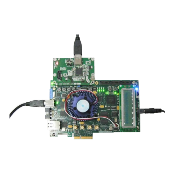
Figure 1 1 1 1 : Altera demo environment for USB3D
Figure
Figure
Figure
: Altera demo environment for USB3D- - - - IP evaluation
: Altera demo environment for USB3D
: Altera demo environment for USB3D
Rev 1.3E / 15 May, 2015
IP evaluation
IP evaluation
IP evaluation
Page 1
Advertisement

Related Manuals for DG USB3D-IP


Summary of Contents for DG USB3D-IP
- Page 1 Device function IP) demo manual Rev 1.3E / 15 May, 2015 This document describes USB3D-IP (USB3.0 device function IP-Core) evaluation procedure using Altera evaluation board (CycloneIV GX board, CycloneVE board, and ArriaV GX starter board) or Xilinx evaluation board (SP605, ML605, KC705, and ZC706 board) and USB3.0 adapter board with evaluation sof-file or bit-file 1 1 1 1 .
- Page 2 dg_usb3.0_dev_ip_demo_instruction_en.doc 1 1 1 1 - - - - 2 2 2 2 Xilinx Xilinx Environment Environment Xilinx Xilinx Environment Environment For Xilinx USB3.0 Device-IP evaluation, user must arrange following environment. Xilinx evaluation board (SP-605 in this example) • USB3.0 adapter board from DesignGateway [Part# AB07-USB3FMC] •...
-
Page 3: Evaluation Procedure
dg_usb3.0_dev_ip_demo_instruction_en.doc 2 2 2 2 ..Evaluation procedure Evaluation procedure Evaluation procedure Evaluation procedure 2 2 2 2 - - - - 1 1 1 1 Altera E Altera E Altera Evaluation Procedure Altera E valuation Procedure valuation Procedure valuation Procedure For Altera USB3.0 Device-IP evaluation, follow evaluation procedure below. - Page 4 dg_usb3.0_dev_ip_demo_instruction_en.doc Figure Figure Figure Figure 4 4 4 4 : Adapter board connection to CycloneVE board : Adapter board connection to CycloneVE board : Adapter board connection to CycloneVE board : Adapter board connection to CycloneVE board Figure Figure Figure Figure 5 5 5 5 : Adapter board connection to ArriaV GX starter board : Adapter board connection to ArriaV GX starter board : Adapter board connection to ArriaV GX starter board...
- Page 5 dg_usb3.0_dev_ip_demo_instruction_en.doc Power up all boards, run ALTERA Programmer on the PC, and download evaluation sof-file to the • FPGA. After download finish, close Programmer software. (At this timing, (FPGA operation is already running and FPGA is waiting JTAG UART output.) Run nios2-terminal from “ALTERA NIOS2 Command Shell”...
- Page 6 dg_usb3.0_dev_ip_demo_instruction_en.doc After sof-file download finish and JTAG UART operation start, check USER_LED0-3 status near by • HSMC connector on the Altera board. See Table 1 for LED definition. Note that LED0 blinks and other LEDs are OFF when USB cable is unplugged. When USB cable is connected again, LED will change its state as shown in Figure 8.
- Page 7 dg_usb3.0_dev_ip_demo_instruction_en.doc After FPGA operation starts, at least following Figure 9 message will appear on the serial console. • Figure Figure 9 9 9 9 : Mass Storage Class operation start message Figure Figure : Mass Storage Class operation start message : Mass Storage Class operation start message : Mass Storage Class operation start message 15 May 2015...
- Page 8 dg_usb3.0_dev_ip_demo_instruction_en.doc 2 2 2 2 - - - - 2 2 2 2 Xilinx Xilinx E E E E valuation Procedure valuation Procedure Xilinx Xilinx valuation Procedure valuation Procedure For Xilinx USB3.0 Device-IP evaluation, follow evaluation procedure below. Check that both Xilinx board (SP605/ML605/KC705/ZC706 board) and adapter board are powered •...
- Page 9 dg_usb3.0_dev_ip_demo_instruction_en.doc Figure Figure 11 Figure Figure 11 11 11: Adapter board connection to ML605 : Adapter board connection to ML605 : Adapter board connection to ML605 : Adapter board connection to ML605 Figure Figure Figure Figure 12 12: Adapter board connection to KC705 : Adapter board connection to KC705 : Adapter board connection to KC705 : Adapter board connection to KC705...
- Page 10 dg_usb3.0_dev_ip_demo_instruction_en.doc Figure 13 Figure 13: Adapter board connection to ZC706 : Adapter board connection to ZC706 Figure Figure : Adapter board connection to ZC706 : Adapter board connection to ZC706 Power up all demo device, run serial terminal (TeraTerm for example) and set following •...
- Page 11 dg_usb3.0_dev_ip_demo_instruction_en.doc Figure Figure 16 Figure Figure 16: Run bat file to program bit and elf file on ZC706 board : Run bat file to program bit and elf file on ZC706 board : Run bat file to program bit and elf file on ZC706 board : Run bat file to program bit and elf file on ZC706 board After bit-file download finish, check GPIO_LED0-3 status on Xilinx board.
- Page 12 dg_usb3.0_dev_ip_demo_instruction_en.doc After FPGA operation starts, at least following Figure 18 message will appear on the serial console. • (same meaning of DS4). If Figure 18 message does not appear, check serial (USB mini) cable as well as serial communication parameters. Figure Figure 18 18: Device operation start message...
- Page 13 dg_usb3.0_dev_ip_demo_instruction_en.doc 3 3 3 3 ..Demo operation example Demo operation example Demo operation example Demo operation example The demo design emulates general USB removable drive so that user can check same functions and • operations. However, the demo design has following limitation. (1) The demo design uses on-board 128Mbytes DDR memory and assigns 127Mbytes as a storage memory space.
- Page 14 dg_usb3.0_dev_ip_demo_instruction_en.doc Device Manager User can confirm by the device manager of Windows that demo drive is recognized as an USB mass storage device. Figure Figure 21 Figure Figure 21: Mass Storage USB Device detected from Device Manager : Mass Storage USB Device detected from Device Manager : Mass Storage USB Device detected from Device Manager : Mass Storage USB Device detected from Device Manager Copy &...
- Page 15 dg_usb3.0_dev_ip_demo_instruction_en.doc Benchmark test User can execute benchmark test to check performance. Note that if HostPC performance is poor (for example of 1-lane PCIe adapter usage or PCIe is GEN1 case), demo drive cannot provide USB3.0 performance. Real transfer performance depends on OS type on the HostPC, CPU performance, and/or PCIe bus speed of the USB3.0 adapter card.
-
Page 16: Revision History
dg_usb3.0_dev_ip_demo_instruction_en.doc Revision History Revision History Revision History Revision History 4 4 4 4 ..Revision Date Description 18-Jul-2012 Release English version. 1.1E 04-Mar-2015 Merged both Altera and Xilinx into one document 1.2E 09-Mar-2015 Updated Figure-15 by the latest test result 1.3E 15-May-2015 Add board support...
Need help?
Do you have a question about the USB3D-IP and is the answer not in the manual?
Questions and answers