Table of Contents
Advertisement
Quick Links
Please note that Cypress is an Infineon Technologies Company.
The document following this cover page is marked as "Cypress" document as this is the
company that originally developed the product. Please note that Infineon will continue
to offer the product to new and existing customers as part of the Infineon product
portfolio.
Continuity of document content
The fact that Infineon offers the following product as part of the Infineon product
portfolio does not lead to any changes to this document. Future revisions will occur
when appropriate, and any changes will be set out on the document history page.
Continuity of ordering part numbers
Infineon continues to support existing part numbers. Please continue to use the
ordering part numbers listed in the datasheet for ordering.
www.infineon.com
Advertisement
Table of Contents

Related Manuals for Infineon Cypress S6SBP501A00VA1001


Summary of Contents for Infineon Cypress S6SBP501A00VA1001
- Page 1 The document following this cover page is marked as “Cypress” document as this is the company that originally developed the product. Please note that Infineon will continue to offer the product to new and existing customers as part of the Infineon product portfolio.
- Page 2 S6SBP501A00VA1001, S6SBP502A00VA1001 Automotive PMIC Evaluation Kit Operation Guide Doc. No. 002-08766 Rev. *E Cypress Semiconductor 198 Champion Court San Jose, CA 95134-1709 www.cypress.com...
- Page 3 Copyrights © Cypress Semiconductor Corporation, 2015-2019. This document is the property of Cypress Semiconductor Corporation and its subsidiaries (“Cypress”). This document, including any software or firmware included or referenced in this document (“Software”), is owned by Cypress under the intellectual property laws and treaties of the United States and other countries worldwide.
- Page 4 Preface This manual explains how to use the evaluation board. Be sure to read this manual before using the product. For this product, consult Cypress sales representatives or support representatives. Handling and use Handling and use of this product and notes regarding its safe use are described in the manual. Follow the instructions in the manual to use this product.
- Page 5 Cautions Caution of the products described in this document The following precautions apply to the product described in this manual. Indicates a potentially hazardous situation which could result in death or serious injury and/or a WARNING fault in the user’s system if the product is not used correctly. Before performing any operation described in this manual, turn OFF all power supplies to the Electric shock, system.
- Page 6 Cautions When turning the power on or off, follow the relevant procedure as described in this document. Before turning the power on, in particular, be sure to finish making all the required connections. Damage Furthermore, be sure to configure and use the product by following the instructions given in this document.
-
Page 7: Table Of Contents
Contents Description .................................. 7 Evaluation Board Specification ..........................8 Pin Descriptions ................................. 9 Input/Output Pin and Pin Socket Descriptions ....................9 Jumper and Pin Socket Descriptions ........................ 10 Setup ..................................11 Connecting ............................... 11 Verification ................................ 11 Layout ..................................12 Component Layout ............................ -
Page 8: Description
1. Description S6SBP501A00VA1001 and S6SBP502A00VA1001 are evaluation kits for the power block of an automotive instrument cluster. These boards implement the Cypress power management IC S6BP501A and S6BP502A, respectively. Figure 1-1. Evaluation Board Block Diagram S6SBP501A00VA1001 S6SBP502A00VA1001 VBATf π Type Filter DC Power Supply PG ND1f 4.5V to 42V... -
Page 9: Evaluation Board Specification
2. Evaluation Board Specification Table 2-1. Evaluation Board Specification Item Symbol Min. Typ. Max. Unit Input Voltage VOUT3V 3.30 Output Voltage VOUT5V 5.00 VOUT1V 1.15 S6SBP501A00VA1001 IOUT3 Output Current IOUT5 IOUT1 VOUT3V 3.30 Output Voltage VOUT5V 5.00 VOUT1V 1.20 S6SBP502A00VA1001 IOUT3 Output Current IOUT5... -
Page 10: Pin Descriptions
3. Pin Descriptions Input/Output Pin and Pin Socket Descriptions Table 3-1. Input/Output Pin Descriptions Connecter Symbol Function Description VBATf DC power supply terminal VOUT3Vf DD3V via load switch output terminal VOUT5Vf DD5V DC/DC convertor output terminal VOUT1Vf DD1V DC/DC convertor output terminal PGNDf, PGND3Vf, PGND5Vf, PGND1Vf Ground terminal EN3V... -
Page 11: Jumper And Pin Socket Descriptions
Pin Descriptions Jumper and Pin Socket Descriptions Table 3-2. Jumper Descriptions Jumper Description Initial Setting Shorted VB or GND to ENSS. Not mounted R23 Short: Shorted between VB and ENSS. SSCG function is ON. R24 Short: Shorted between GND and ENSS. SSCG function is OFF. Short R23 and R24 must not be shorted simultaneously. -
Page 12: Setup
4. Setup Connecting Connect the board to the power supply, load equipment, and voltage meter as shown in Figure 4-1. Figure 4-1. Connecting the Board and Equipment Voltage Load Meter Voltage Meter Load Voltage Meter Load +12V Power Supply Verification Insert pin sockets of EN1V, EN3V, and EN5V. -
Page 13: Layout
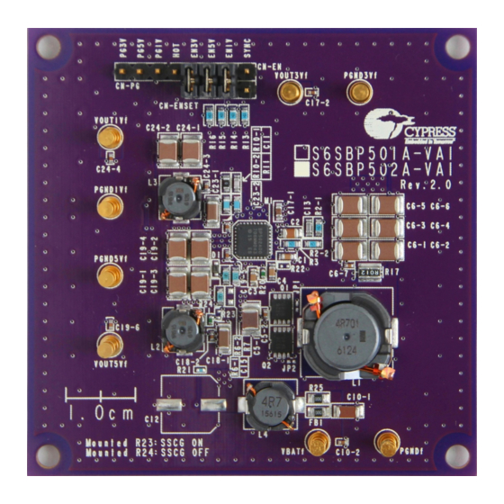
5. Layout Component Layout Figure 5-1. Evaluation Board Component Layout Layer1 Top View Layer4 Top View Board size: 65mm × 65mm S6SBP501A00VA1001, S6SBP502A00VA1001 Automotive PMIC Evaluation Kit Operation Guide, Doc. No. 002-08766 Rev. *E... -
Page 14: Wiring Layout
Layout Wiring Layout Figure 5-2. Evaluation Board Wiring Layout layer 1 Top View layer 2 Top View layer 4 Top View layer 3 Top View S6SBP501A00VA1001, S6SBP502A00VA1001 Automotive PMIC Evaluation Kit Operation Guide, Doc. No. 002-08766 Rev. *E... -
Page 15: Circuit Schematic
6. Circuit Schematic S6SBP501A00VA1001, S6SBP502A00VA1001 Automotive PMIC Evaluation Kit Operation Guide, Doc. No. 002-08766 Rev. *E... - Page 16 Figure 6-1. Evaluation Board Circuit Schematic VBATf + C10-2 C10-1 PGNDf VOUT5V C5-2 C5-1 BST3V 14 DRVH3V R2-1 R2-2 C6-1 C6-3 C6-5 C6-7 LX3V 16 FB3V DRVL3V PGND3V C6-2 C6-4 C6-6 IN3V VOUT3V VOUT3Vf PGND3Vf C17-1 C17-2 VOUT5V R6-1 R6-2 C19-1 C-19-3 C19-5...
-
Page 17: Component List
7. Component List Table 7-1. Evaluation Board Component List Rated Rated Component Part Number Vendor Value Voltage Current Remarks CGA3E2X7R1H104K080AA 0.1 µF CGA4J3X7R1C475K125AB 4.7 µF CGA3E2X7R1H104K080AA 0.1 µF CGA3E2X7R1H104K080AA 0.1 µF C5-1 CGA6P3X7S1H106M250AB 10 µF C5-2 CGA2B3X7R1H104K050BB 0.1 µF C6-1 CGA6P1X7R1C226M250AC 22 µF C6-2... - Page 18 Component List Rated Rated Compone Current Parts Number Vendor Value Voltage Remarks C23-1 CGA5L1X7R1C106K160AC 10 µF C23-2 CGA2B3X7R1H104K050BB 0.1 µF C24-1 CGA6P1X7R1C226M250AC 22 µF C24-2 CGA6P1X7R1C226M250AC 22 µF C24-3 CGA2B3X7R1H104K050BB 0.1 µF C24-4 CGA2B3X7R1H104K050BB 0.1 µF RB521S30T1G Semi RK73Z2A 0Ω CLF12577NIT-4R7N-D 4.7 µH CLF6045NIT-1R5N-D...
- Page 19 Component List Rated Rated Compone Current Parts Number Vendor Value Voltage Remarks RK73Z2A 0Ω TDK Corporation ON Semi ON Semiconductor Cypress Cypress Semiconductor Corp KOA Corporation Panasonic Corporation Pana SUSUMU CO., LTD. NMT: No mount. These components are compliant with RoHS, and ask each vendor for details if necessary. S6SBP501A00VA1001, S6SBP502A00VA1001 Automotive PMIC Evaluation Kit Operation Guide, Doc.
-
Page 20: Reference Data
8. Reference Data This chapter provides the DC\DC converter characteristics of S6SBP502A00VA1001. DC Characteristics 8.1.1 Conversion Efficiency VOUT5V VOUT3V VOUT1V Ta=+25℃, VBAT=12V, Ta=+25℃, VBAT=12V, Ta=+25℃, VBAT=12V, EN5V=VIN, EN1V=EN3V=GND EN5V=VIN, EN1V=GND, EN3V=VB EN5V=VIN, EN1V=VB, EN3V=GND VOUT5V VOUT3V VOUT1V Ta=+25℃, IOUT5=0.65A, Ta=+25℃, IOUT3=0.95A, Ta=+25℃, IOUT1=1A, EN5V=VIN, EN1V=EN3V=GND, EN5V=VIN, EN1V=GND, EN3V=VB,... -
Page 21: Regulations
Reference Data 8.1.2 Regulations Ta=+25℃, VBAT=12V, Ta=+25℃, VBAT=12V, Ta=+25℃, VBAT=12V, EN5V=VIN, EN1V=GND, EN3V=VB EN5V=VIN, EN1V=VB, EN3V=GND EN5V=VIN, EN1V=EN3V=GND Ta=+25℃, IOUT5=0.65A, Ta=+25℃, IOUT3=0.95A, Ta=+25℃, IOUT1=1A, EN5V=VIN, EN1V=EN3V=GND, EN5V=VIN, EN1V=GND, EN3V=VB, EN5V=VIN, EN1V=VB, EN3V=GND, SYNC=GND SYNC=GND SYNC=GND VBAT=12V, IOUT5=0.65A, VBAT=12V, IOUT3=0.95A, VBAT=12V, IOUT1=1A, EN5V=VIN, EN1V=EN3V=GND, EN5V=VIN, EN1V=GND, EN3V=VB, EN5V=VIN, EN1V=VB, EN3V=GND,... -
Page 22: Waveforms
Reference Data Waveforms 8.2.1 Start-up and Stop 5ms/div 5ms/div VBAT (5V/div) VOUT5V (2V/div) PG5V (5V/div) IN3V (DD3V output 2V/div) EN5V=VIN, EN3V=EN1V=GND, SYNC=GND, IOUT5=0A 5ms/div 5ms/div EN3V (5V/div) VOUT3V (2V/div) PG3V (5V/div) VBAT=12V, EN5V=VIN, EN1V=GND, SYNC=GND, IOUT5=IOUT3=0A 5ms/div 5ms/div EN1V (5V/div) VOUT1V (1V/div) PG1V (5V/div) VBAT=12V, EN5V=VIN, EN3V=GND, SYNC=GND, IOUT5=IOUT1=0A... -
Page 23: Switching Waveform
Reference Data 8.2.2 Switching Waveform LX5V 5us/div 200ns/div LX5V (1V/div) (1V/div) VBAT=12V, EN5V=VIN, EN3V= EN1V=GND, VBAT=12V, EN5V=VIN, EN3V= EN1V=GND, SYNC=GND, IOUT5=50mA SYNC=GND, IOUT5=1.3A 1us/div LX3V (2V/div) LX3V (2V/div) 20us/div VBAT=12V, EN5V=VIN, EN3V=VB, EN1V=GND, VBAT=12V, EN5V=VIN, EN3V=VB, EN1V=GND, SYNC=GND, IOUT5=0A, IOUT3=100mA SYNC=GND, IOUT5=0A, IOUT3=1.9A SSCG off LX1V (1V/div) -
Page 24: Output Ripple Waveform
Reference Data 8.2.3 Output Ripple Waveform 1us/div 1us/div VOUT5V (50mV/div) VOUT3V (20mV/div) VBAT=12V, EN5V=VIN, EN3V=EN1V=VB, VBAT=12V, EN5V=VIN, EN3V=EN1V=VB, SYNC=GND, IOUT5=1.3A, IOUT3=IOUT1=0A SYNC=GND, IOUT5=0A, IOUT3=1.9A, IOUT1=0A 1us/div 500us/div VOUT5V (50mV/div) VOUT3V (20mV/div) VOUT1V (10mV/div) VOUT1V (10mV/div) VBAT=12V, EN5V=VIN, EN3V=EN1V=VB, SYNC=GND, IOUT5=IOUT3=0A, IOUT1=2A VBAT=12V, EN5V=VIN, EN3V=EN1V=VB, SYNC=GND, IOUT5=IOUT3=IOUT1=0A 1us/div... -
Page 25: Load Transient Waveforms
Reference Data 8.2.4 Load Transient Waveforms 100us/div 100us/div VOUT5V (500mV/div) VOUT3V (200mV/div) IOUT5 0A<->1.3A (1A/div) IOUT3 0A<->1.9A (1A/div) VBAT=12V, EN5V=VIN, EN3V=EN1V=VB, VBAT=12V, EN5V=VIN, EN3V=EN1V=VB, SYNC=GND, IOUT3=IOUT1=0A SYNC=GND, IOUT3=IOUT1=0A 100us/div VOUT1V (100mV/div) IOUT1 0A<->2A (1A/div) VBAT=12V, EN5V=VIN, EN3V=EN1V=VB, SYNC=GND, IOUT5=IOUT3=0A 8.2.5 Line Transient Waveforms 5ms/div VBAT 12V<->3.7V (5V/div) -
Page 26: Protection And Detection Function Waveforms
Reference Data 8.2.6 Protection and Detection Function Waveforms Over current protection of DD1V Over voltage detection of DD5V VOUT5V (500mV/div) 5ms/div 20ms/div VOUT1V (500mV/div) Rising to 5.5V Reducing load LX5V (4V/div) resistance PG1V (5V/div) PG5V (5V/div) IOUT1 (1A/div) LX3V (10V/div) Under voltage detection of DD1V VBAT=12V, EN5V=VIN, EN3V=GND, EN1V=VB, VBAT=12V, EN5V=VIN, EN3V=EN1V=GND, SYNC=GND,... -
Page 27: Ac Characteristics
Reference Data AC Characteristics 8.3.1 Gain-Phase Characteristics DD5V Gain Phase Band width: 29kHz VBAT=12V, EN5V=VIN, Phase margin: 58degree -135 EN3V=EN1V=GND, -180 SYNC=GND, IOUT5=1.3A, 1000 10000 100000 1000000 Frequency(Hz) DD3V Gain Phase Band width: 37kHz VBAT=12V, EN5V=VIN, -135 Phase margin: 31degree EN3V=VB, EN1V=GND, -180 SYNC=GND, IOUT5=0A, IOUT3=1.9A... -
Page 28: Temperature
Reference Data Temperature =+25℃, VBAT=12V, EN5V=VIN, EN3V= EN1V=VB, =+25℃, VBAT=12V, EN5V=VIN, EN3V= EN1V=VB, Half load: IOUT5=0.65A, IOUT3=0.95A, IOUT1=1A, Full load: IOUT5=1.3A, IOUT3=1.9A, IOUT1=2A, SYNC=GND SYNC=GND EMI (Radiated Emissions Example) VBAT=12V, EN5V=VIN, EN3V= EN1V=VB, IOUT5=1.3A, IOUT3=1.9A, IOUT1=2A, SYNC=GND, SSCG=ON Measured in ALSE S6SBP501A00VA1001, S6SBP502A00VA1001 Automotive PMIC Evaluation Kit Operation Guide, Doc. -
Page 29: Ordering Information
9. Ordering Information Table 9-1. Ordering Information Part Number EVB Revision Note S6SBP501A-VA1 S6SBP501A00VA1001 Mounted IC: S6BP501A00SN2B000 S6SBP502A-VA1 S6SBP502A00VA1001 Rev 2.0 Mounted IC: S6BP502A00SN2B000 S6SBP501A00VA1001, S6SBP502A00VA1001 Automotive PMIC Evaluation Kit Operation Guide, Doc. No. 002-08766 Rev. *E... -
Page 30: Document Revision History
Revision History Document Revision History Document Title: S6SBP501A00VA1001, S6SBP502A00VA1001 Automotive PMIC Evaluation Kit Operation Guide Document Number: 002-08766 Revision Issue Date Description of Change 09/25/2015 Initial release 02/04/2016 Migrated Spansion guide from S6SBP501A00VA1001_SS901-00044-1v0-E to Cypress format 12/20/2016 Changed VOUT1f output voltage of S6SBP501A00VA1001 Changed some compoments.
Need help?
Do you have a question about the Cypress S6SBP501A00VA1001 and is the answer not in the manual?
Questions and answers