Table of Contents
Advertisement
Quick Links
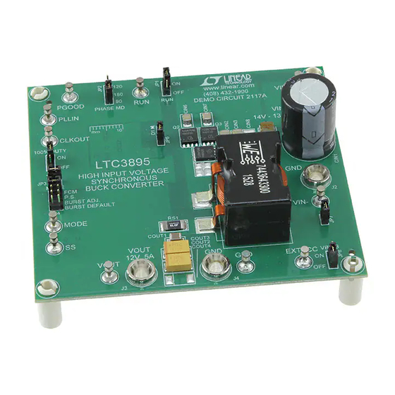
Description
Demonstration circuit 2117A is a single output high volt-
age nonisolated synchronous step-down converter that
drives all N-channel MOSFET power stage. It features the
LTC3895EFE, a high voltage step-down DC/DC controller
housed in a TSSOP-38 package with several pins removed
for high voltage spacing.
This DC2117A operates over an input voltage range from
14V to 130V, while the
LTC
This demo board produces a 12V output voltage with up to
a 5A output current, and is configured with a sense resistor
for over current protection and has optional DCR sensing.
To prevent high on-chip power dissipation in high input
voltage applications, the LTC3895 includes an NDRV pin
which drives the gate of an optional external N-channel
MOSFET acting as a low dropout linear regulator to supply
IC power and is an option on this board.
An internal charge pump allows for 100% duty cycle op-
eration in dropout, a useful feature when powered from
a battery during discharge. The LTC3895's powerful 1Ω
performance summary
Table 1.
PARAMETER
Input Voltage Range
Output Voltage V
OUT
Maximum Output Current I
OUT(MAX)
Default Operating Frequency (Typical)
External Clock Sync Frequency Range
Typical Full Load Efficiency (See Figure 4)
*Important Note: 60V or higher voltage can result in an electric shock if care is not taken. Also, hot plugging the circuit to a power supply that has more
than 40V present at its output can produce a high voltage transient exceeding the absolute maximum input voltage which can damage the DC2117A
board.
3895
can operate up to 150V.
®
Specifications are at T
CONDITIONS
DC Up to 150V
V
= 14~130V, I
IN
V
= 14~130V
IN
V
= 48V, V
IN
OUT
DEMO MANUAL DC2117A
High Input Voltage
Synchronous Buck Converter
N-channel MOSFET gate drivers can be adjusted from
5V to 10V to enable the use of logic- or standard-level
MOSFETs to maximize efficiency. The EXTV
the LTC3895 to be powered from the output of the switch-
ing regulator or other available source, reducing power
dissipation and improving efficiency.
A mode selector allows the DC2117A to operate in forced
continuous operation, pulse-skipping or low ripple Burst
Mode
operation during light loads. Additional features
®
include a power good output signal, a PLLIN, PHASEMD
and CLKOUT for multiphase operation.
The LTC3895 data sheet gives a complete description of
the part, operation and application information and must
be read in conjunction with this demo board manual.
Design files for this circuit board are available at
http://www.linear.com/demo/DC2117A
L, LT, LTC, LTM, Linear Technology, Burst Mode and the Linear logo are registered trademarks
of Linear Technology Corporation. All other trademarks are the property of their respective
owners.
= 25°C
A
Transient
PK
= 0~5A, JP4: FCM
OUT
= 12V, I
= 5A, f
= 150kHz
OUT
SW
LTC3895EFE
pin permits
CC
UNITS
14V ~ 130V
12V ± 2% (11.76V ~ 12.24V)
5A
150kHz
75kHz to 850kHz
94.9%
dc2117af
1
Advertisement
Table of Contents

Subscribe to Our Youtube Channel
Related Manuals for Linear Technology DC2117A


Summary of Contents for Linear Technology DC2117A
- Page 1 *Important Note: 60V or higher voltage can result in an electric shock if care is not taken. Also, hot plugging the circuit to a power supply that has more than 40V present at its output can produce a high voltage transient exceeding the absolute maximum input voltage which can damage the DC2117A board.
-
Page 2: Quick Start Procedure
DEMO MANUAL DC2117A Quick start proceDure Demonstration circuit DC2117A is easy to set up to evalu- 2. With power off, connect the input power supply to V ate the performance of the LTC3895EFE. Refer to Figure 1 and GND. for proper measurement equipment setup and follow the 3. -
Page 3: Frequency Synchronization And Mode Selection
PLLIN turret. Depending converter to run in forced continuous operation, pulse- upon the JP4 setting, the DC2117A will operate in different skipping operation, Burst Mode operation or Burst Mode modes. See Table 2 for the detailed description. -
Page 4: Low Quiescent Current Applications And Measurement
40µA in sleep mode as specified in the LTC3895 data value FB divider resistors should be used. In addition, some sheet. However, the input current of the DC2117A board jumpers and resistors should be configured accordingly. can be higher than this value because of additional circuit Refer to Table 4 for the low input quiescent current setup. - Page 5 DEMO MANUAL DC2117A eXtV Bias supply By default, the DC2117A EXTV turret is tied to the 12V Alternatively, EXTV can also be powered by an external to save IC power loss. power supply: To power the EXTV from onboard bias supply: 1.
- Page 6 DEMO MANUAL DC2117A eXtV Bias supply 20MHz BW 100mV/DIV 200µs/DIV DC2117a F04 Figure 4. DC2117A V 1.25A ~ 2.5A Load Transient at V = 48V 20MHz BW 100mV/DIV 200µs/DIV DC2117a F05 Figure 5. DC2117A V 1.25A ~ 2.5A Load Transient at V...
-
Page 7: Parts List
DEMO MANUAL DC2117A parts list ITEM REFERENCE PART DESCRIPTION MANUFACTURER/PART NUMBER Required Circuit Components CIN1 CAP , 100µF 20% 200V ELEC NIC NRB-XS101M200V16x20TBF CIN2, CIN3, CIN4, CIN5, C14 CAP , 1812 0.47µF 10% 200V X7R MURATA GRM43DR72E474KW01L CIN6, CIN7 CAP , 1210 0.1µF 10% 200V X7R... - Page 8 DEMO MANUAL DC2117A parts list ITEM REFERENCE PART DESCRIPTION MANUFACTURER/PART NUMBER Additional Demo Board Circuit Components CIN8 CAP , 1812 OPTION OPTION COUT4 CAP , 7343 OPTION OPTION C1, C5, C8, C16 CAP , 0603 OPTION OPTION D1, D2 DIODE, OPTION...
-
Page 9: Schematic Diagram
Information furnished by Linear Technology Corporation is believed to be accurate and reliable. However, no responsibility is assumed for its use. Linear Technology Corporation makes no representa- tion that the interconnection of its circuits as described herein will not infringe on existing patent rights. - Page 10 Linear Technology Corporation (LTC) provides the enclosed product(s) under the following AS IS conditions: This demonstration board (DEMO BOARD) kit being sold or provided by Linear Technology is intended for use for ENGINEERING DEVELOPMENT OR EVALUATION PURPOSES ONLY and is not provided by LTC for commercial use. As such, the DEMO BOARD herein may not be complete in terms of required design-, marketing-, and/or manufacturing-related protective considerations, including but not limited to product safety measures typically found in finished commercial goods.
Need help?
Do you have a question about the DC2117A and is the answer not in the manual?
Questions and answers