Advertisement
Quick Links
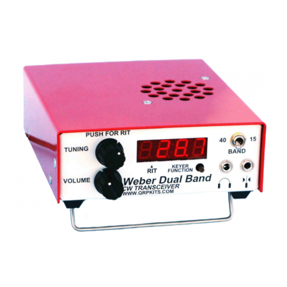
Dual Band HF CW transceiver
Hendricks kits and KD1JV Designs
QRPKITS.COM
Specifications:
Any two ham bands, 80, 40, 30, 20, 17 or 15 meters, choose at time of order.
5 watts output on all bands with 13.8V supply
Built in Iambic keyer with 5 to 40 wpm code speed, selectable Iambic A or B modes and two 63 character
message memories.
Receiver sensitivity, 0.2 uV MSD
DDS VFO for rock steady stability with 50 Hz and 200 Hz tuning rates
Easy to read four digit LED display with leading zero suppression.
Rotary knob tuning
RIT (receive incremental tuning)
Four IF crystals for excellent selectivity and opposite side band rejection
600 Hz audio filter
Audio derived AGC circuit
500 mw audio amplifier with built in speaker
Small size, 4.6" wide, 1.6" tall and 5.5" deep.
Light weight, 13 ounces.
Modest supply current requirements, 55 ma on receive (no signal) and 550 to 750 ma on transmit at 5W out
(current depends on band, higher bands draw more current)
1
Advertisement

Subscribe to Our Youtube Channel
Related Manuals for QRPKits Weber Dual Band


Summary of Contents for QRPKits Weber Dual Band
- Page 1 Dual Band HF CW transceiver Hendricks kits and KD1JV Designs QRPKITS.COM Specifications: Any two ham bands, 80, 40, 30, 20, 17 or 15 meters, choose at time of order. 5 watts output on all bands with 13.8V supply Built in Iambic keyer with 5 to 40 wpm code speed, selectable Iambic A or B modes and two 63 character message memories.
- Page 2 Assembly Instructions: The quickest and easiest way to build the rig is in “layers”. The lowest profile parts are installed first, such as resistors and diodes, then higher profile parts such as capacitors and so on. Once the board is populated with all the parts, testing will be done by inserting the various Integrated Circuit chips one at a time and testing the associated stage they are used with.
- Page 3 Parts placement guide. (color) Silk screen of Q10 missing from board.
- Page 4 Parts placement diagram, inkjet friendly. Parts with no value indicated have band specific values. Q10 silk screen missing from board.
- Page 5 Assembled board, mounted in case. Speaker mounting:...
- Page 6 Part by part placement guide: Resistors √ √ location Value Color code Location Value Color code 100 K BRN/BLK/YEL/GLD RED/VOL/BRN/GLD 47 K YEL/VOL/ORG/GLD RED/VOL/BRN/GLD GRN/BRN/BLK/GLD 1 MEG BRN/BLK/GRN/GLD 100 K BRN/BLK/YEL/GLD BRN/BLK/RED/GLD RED/VOL/BRN/GLD 2.2 K RED/RED/RED/GLD RED/VOL/BRN/GLD 1 MEG BRN/BLK/GRN/GLD YEL/VOL/BRN/GLD BRN/BLK/RED/GLD 3.9 K...
- Page 7 Capacitors: There are four types of capacitors used. ● Multi-layer (MONO) caps, which are generally yellow and rectangular is shape. ● NPO type disks will have a black dot on the top edge of the cap. Note. Some of the ceramic disk caps will have lead spacing wider then the hole spacing on the board.
- Page 8 0.1 ufd (104) MONO, YELLOW 0.1 ufd (104) MONO, YELLOW .001 ufd (102) DISK, BROWN 0.1 ufd (104) MONO, YELLOW .01 ufd SMT, PREINSTALLED .001 ufd (102) DISK, BROWN 0.01 ufd (103) FILM, GREEN 10 ufd/16 or 25V ELECTROLYTIC 0.47 ufd/16 or 25V ELECTROLYTIC 0.1 ufd (104) MONO, YELLOW...
-
Page 9: Band Specific Parts
Band specific parts: In the color parts layout, the transmitter low pass filter and associated receiver input parts are filled in with the same color. Band “A” parts are colored in light blue and Band “B” is colored in dark blue. It doesn't matter which specific band you call “A” and which you call “B”, that will be programmed later. - Page 10 T1/T2 winding: Hold the core in your left hand and start winding by passing 1/2” of the magnet wire up through the “bottom” side of the core as shown in the diagram. Then continue winding the remaining required number of turns by passing the long end of the wire in and down from the top of the core. When you get to the end of the required number of secondary turns, make about a 1/2”...
- Page 11 The speaker is wired to the two pads labeled “G” and “HP” at the front, left hand side of the main board. Paddle jack wiring is shown in the diagram below. The wires should be about 2” long so that the jack will reach the front panel for mounting later.
- Page 12 Calibration of DDS reference frequency and LO frequency: Calibration of the reference frequency and LO frequency is not absolutely necessary, but will improve the performance of the rig. If an accurate frequency counter and audio oscilloscope , either CRT or PC based, is not available, do not attempt calibration.
- Page 13 along the top edge of the board on either side of the display. • Install the BNC jack and connect to the wires from the main board. HINT: To keep the BNC jack from spinning as you tighten the nut, put a BNC plug on the jack and hold that firmly. •...
-
Page 14: Troubleshooting Guide
Trouble shooting guide: In most cases, any problems with the getting the rig to work will be tracked down to soldering problems or miss placed parts. A close visual inspection of the board is often enough to find soldering problems or the miss-placed parts. Soldering problems fall into four groups: Missing solder connections Solder bridges between closely spaced pads which should not be connected togther. -
Page 15: Operation
Operation: FRONT PANEL CONTROLS Power up: Upon power up, the display will first show a display test, lighting all LED digit segments and decimal points for a couple of seconds. The display will then indicate the selected operating band for another couple of seconds. Finally, the initial operating frequency is shown and the rig is ready to operate. - Page 16 Tune Up Mode: Clicking and holding closed the keyer switch for 1 second will access the “Tune Up Mode” function. Release the switch after the side tone annunciates the Morse letter “T” to activate this function. A character resembling a “t” will appear on the display to indicate this mode is active.
-
Page 17: Power Supply
determined by which paddle was closed first. The difference between A and B modes is what happens after the paddles are released. In A mode, the keyer simply stops sending. In B mode, an extra and opposite element is sent from the last element being sent when the paddles are released. - Page 18 Receiver circuits schematic:...
- Page 19 MPU/Transmitter/Front panel schematic:...
- Page 20 How it works: Signals from the antenna first pass through the transmitters Low Pass Filter, which are selected for the current operating band by two relays, RY1 and RY2. The receiver signal is picked off from the drains of the transmitters PA FETs and routed through a QSK switch, Q6 a 2N7000 MOSFET.
- Page 21 Q10, a P channel power MOSFET switches the supply voltage to the PA. The gate pull up resistor R1 in conjunction with C10 slows down the turn on and off times to provide the proper voltage ramp. Q1 connected back to the uP is used to turn Q10 on and off for keying.
Need help?
Do you have a question about the Weber Dual Band and is the answer not in the manual?
Questions and answers