
Related Manuals for NXP Semiconductors freescale semiconductor MC13211


Summary of Contents for NXP Semiconductors freescale semiconductor MC13211
- Page 1 MC13211/212/213 ™ ZigBee - Compliant Platform 2.4 GHz Low Power Transceiver for the ® IEEE 802.15.4 Standard plus Microcontroller Reference Manual Document Number: MC1321xRM Rev. 1.6 05/2010...
- Page 2 How to Reach Us: Information in this document is provided solely to enable system and software implementers to use Freescale Semiconductor products. There are no express or implied copyright licenses granted Home Page: hereunder to design or fabricate any integrated circuits or integrated circuits based on the information www.freescale.com in this document.
-
Page 3: Table Of Contents
Contents About This Book Audience ..............xv Organization . - Page 4 Test Pin SM ..............3-3 Internal Functional Interconnects and System Reset .
- Page 5 Modem SPI Basic Operation ........... 4-3 4.5.1 Modem SPI Pin Definition .
- Page 6 5.13 CLKO_Ctl - Register 0A ........... . . 5-15 5.14 GPIO_Dir - Register 0B .
- Page 7 6.7.3 Timer-Triggered Transceiver Events ......... . 6-6 Chapter 7 Modem Modes of Operation Modem Operational Modes Summary .
- Page 8 9.2.6 GPIO in Off, Hibernate, and Doze Modes ........9-3 Crystal Oscillator .
- Page 9 11.6.2 FLASH Options Register (FOPT and NVOPT) ....... . 11-17 11.6.3 FLASH Configuration Register (FCNFG) .
- Page 10 13.4.2 Internal Pullup Control ........... . 13-7 13.4.3 Slew Rate Control .
- Page 11 14.5.5 Filter Registers (FLTU, ICGFLTL) ......... 14-23 14.5.6 Trim Register (TRM).
- Page 12 17.2 TPM Block Diagram............17-1 17.3 Pin Descriptions .
- Page 13 18.9.6 SCI1 Control Register 3 (SCIxC3) ......... . 18-15 18.9.7 SCI1 Data Register (SCIxD).
- Page 14 20.6 ATD Registers and Control Bits ..........20-9 20.6.1 ATD Control (ATDC) .
-
Page 15: Audience
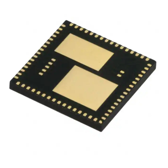
About This Book ™ This manual describes Freescale’s second-generation ZigBee platform (the MC1321x family) which incorporates a low power 2.4 GHz radio frequency transceiver and an 8-bit microcontroller into a single 9x9x1 mm 71-pin LGA package. The MC1321x solution can be used for wireless applications from simple proprietary point-to-point connectivity, to a complete ZigBee mesh network. -
Page 16: Revision History
Chapter 11 MCU Memory — Describes on-chip memory in the HCS08 series of MCUs and shows that it consists of RAM, FLASH program memory for non-volatile data storage, plus I/O and control/status registers. Chapter 12 MCU Resets, Interrupts, and System Configuration — This section discusses basic reset and interrupt mechanisms and the various sources of reset and interrupts in the HCS08. - Page 17 Definitions, Acronyms, and Abbreviations The following list defines the acronyms and abbreviations used in this document. Acknowledgement Frame Application Programming Interface Baseband Clear Channel Assessment Cyclical Redundancy Check Differential Chip Decoding Device Management Entity Frame Check Sequence Full Function Device FFD-C Full Function Device Coordinator Frame Length Indicator...
-
Page 18: References
Serial Peripheral Interface SSCS Service Specific Convergence Layer Software Voltage Controlled Oscillator References The following sources were referenced to produce this book: [1] IEEE 802.15.4 Standard [2] Freescale MC1319x Data Sheet [3] Freescale MC9S08GB/GT60 Data Sheet [4] Freescale MC1321x Data Sheet MC1321x Reference Manual, Rev. -
Page 19: Mc1321X Introduction
Chapter 1 MC1321x Introduction ™ The MC1321x family is Freescale’s second-generation ZigBee platform which incorporates a low power 2.4 GHz radio frequency transceiver and an 8-bit microcontroller into a single 9x9x1 mm 71-pin LGA package. The MC1321x solution can be used for wireless applications from simple proprietary point-to-point connectivity to a complete ZigBee mesh network. - Page 20 MC1321x Introduction NOTE • The MC1321x now uses an updated version of the 689S08A 8-bit microprocessor to correct errata associated with the onboard FLL and reset pin. Refer to the associated errata for this new device, Document Number MSE9S08GB60A_4L11Y, on the Freescale web site. •...
-
Page 21: Ordering Information
MC1321x Introduction Ordering Information Table 1-1 lists additional devices in the MC1321x family. NOTE The device marking for silicon revision 1.1 and newer is different than version 1.0 and older. For more details about the 71-pin LGA package used for the MC1321x family, see the 802.15.4/ZigBee Hardware Design Considerations Reference Manual (ZHDCRM). -
Page 22: Microcontroller Features
MC1321x Introduction Microcontroller Features • Low voltage MCU with 40 MHz low power HCS08 CPU core • Up to 60K flash memory with block protection and security and 4K RAM — MC13211: 16KB Flash, 1KB RAM — MC13212: 32KB Flash, 2KB RAM —... -
Page 23: Rf Modem Features
MC1321x Introduction RF Modem Features • Fully compliant 802.15.4 Standard transceiver supports 250 kbps O-QPSK data in 5.0 MHz channels and full spread-spectrum encode and decode • Operates on one of 16 selectable channels in the 2.4 GHz ISM band •... -
Page 24: Synkrorf Platform
MC1321x Introduction • Supports star, mesh and cluster tree topologies • Supports beaconed networks • Supports GTS for low latency • Multiple power saving modes • AES-128 Security module • 802.15.4 Sequence support • 802.15.4 Receiver Frame filtering. 1.5.3 SynkroRF Platform ®... -
Page 25: Zigbee-Compliant Network Stack
MC1321x Introduction • Channel Agility mechanism • Provides robustness and ease of use • Includes essential functionality to build and support a CE network The BeeStack Consumer layer uses components from the standard HCS08 Freescale platform, which is also used by the Freescale implementations of 802.15.4. MAC or ZigBee™ layers. For more details about the platform components, see the Freescale Platform Reference Manual. -
Page 26: System Block Diagram
MC1321x Introduction System Block Diagram Figure 1-1 shows a simplified block diagram of the MC1321x solution. Analog Background HCS08 CPU Receiver Debug Module RFIC Timers 8 Channel Flash Memory Transmit/ 10 Bit ADC Frequency Balun Receive Generator Digital Control Switch Logic 2x SCI Analog... -
Page 27: Modem Overview
MC1321x Introduction 802.15.4 Modem Overview 1.7.1 Modem Block Diagram VDDA Analog Decimation Baseband Matched Regulator VBATT 2nd IF Mix er Filter Mix er Filter IF = 1 MHz PMA 1st IF Mix er Pow er-Up Digital VDDINT IF = 65 MHz Control Regulator L Logic... -
Page 28: Modem Packet Structure
MC1321x Introduction 1.7.3 Modem Packet Structure Figure 1-3 shows the 802.15.4 Standard compliant packet structure of the MC1321x. Payloads of up to 125 bytes are supported. The MC1321x adds a four-byte preamble, a one-byte Start of Frame Delimiter (SFD), and a one-byte Frame Length Indicator (FLI) before the data. A Frame Check Sequence (FCS) is calculated and appended to the end of the data. -
Page 29: Modem Transmit Path Description
MC1321x Introduction 802.15.4 Accuracy and range Requirements -100 Input Pow er (dBm) Figure 1-4. Reported Power Level versus Input Power in Clear Channel Assessment Mode Figure 1-5 shows energy detection/LQI reported level versus input power. 802.15.4 Accuracy and Range Requirements Input Pow er Level (dBm) Figure 1-5. -
Page 30: Radio Usage
MC1321x Introduction transmitted. In both modes, a two-byte FCS is calculated in hardware from the payload data and appended to the packet. This done without intervention from the user. 1.7.6 Radio Usage The MC1321x RF analog interface has been designed to provide maximum flexibility as well as low external part count and cost. -
Page 31: Mcu Block Diagram
MC1321x Introduction Although detailed information is provided in this reference manual, the user is directed to the HCS08 Family Reference Manual, (HCS08RMv1, Rev. 1) for general family reference. Background information on Development Support and extended Instruction Set Details are especially useful. 1.8.1 MCU Block Diagram INTERNAL BUS... -
Page 32: Hcs08 Central Processing Unit (Cpu)
MC1321x Introduction NOTE The MC1321x MCU has port signals that are not pinned-out. These signals should be initialized to a known condition for low power modes. 1.8.2 HCS08 Central Processing Unit (CPU) The HCS08 CPU is fully source- and object-code-compatible with the M68HC08 CPU. Several instructions and enhanced addressing modes were added to improve C compiler efficiency and to support a new background debug system which replaces the Monitor Mode of earlier M68HC08 microcontrollers (MCU). -
Page 33: Mcu Internal Clock Distribution
MC1321x Introduction • Internal Clock Generator (ICG) - Supports external clock source or external crystal oscillator and has internal reference generator with two controlled sources. One is approximately 8 MHz and can be selected as local clock for background debug controller. The other is typically 243 kHz and can be trimmed for a low-cost MCU clock source •... -
Page 34: System Clock Configuration
MC1321x Introduction • ICGLCLK — Development tools can select this internal self-clocked source (~ 8 MHz) to speed up BDC communications in systems where the bus clock is slow • ICGERCLK — External reference clock can be selected as the real-time interrupt clock source The MCU ICG is described in detail by Chapter 14, “MCU Internal Clock Generator (ICG)”. -
Page 35: Mc1321X Pins And Connections
Chapter 2 MC1321x Pins and Connections Device Pin Assignment PTA3/KBI1P3 PTD4/TPM2CH1 MC1321x PTA4/KBI1P4 PTD2/TPM1CH2 PTA5/KBI1P5 ATTN TES T PTA6/KBI1P6 PTA7/KBI1P7 GPIO1 Flag opening VDDAD GPIO2 PTG0/BKGD/MS GPIO3 GPIO4 PTG1/XTAL PTG2/EXTAL Flag opening PAO_M CLKO PAO_P RES ET PTC0/TXD2 TES T RFIN_P PTC1/RXD2 PTC2/S DA1... -
Page 36: Pin Definitions
MC1321x Pins and Connections Pin Definitions Table 2-1 details the MC1321x pinout and functionality. Table 2-1. Pin Function Description Pin # Pin Name Type Description Functionality PTA3/KBI1P3 Digital MCU Port A Bit 3 / Keyboard Input Bit 3 Input/Output PTA4/KBI1P4 Digital MCU Port A Bit 4 / Keyboard Input Bit 4 Input/Output... - Page 37 MC1321x Pins and Connections Table 2-1. Pin Function Description (continued) Pin # Pin Name Type Description Functionality PTC7 Digital MCU Port C Bit 7 Input/Output PTE0/TXD1 Digital MCU Port E Bit 0 / SCI1 TX data out Input/Output PTE1/RXD1 Digital MCU Port E Bit 1/ SCI1 RX data in Input/Output VDDD...
- Page 38 MC1321x Pins and Connections Table 2-1. Pin Function Description (continued) Pin # Pin Name Type Description Functionality RFIN_P RF Input Modem RF input/output positive When used with internal T/R switch, this (Output) is a bi-directional RF port for the internal LNA and PA Not used May be grounded or left open...
- Page 39 MC1321x Pins and Connections Table 2-1. Pin Function Description (continued) Pin # Pin Name Type Description Functionality PTB3/AD1P3 Input/Output MCU Port B Bit 3 / ATD analog Channel 3 PTB4/AD1P4 Input/Output MCU Port B Bit 4 / ATD analog Channel 4 PTB5/AD1P5 Input/Output MCU Port B Bit 5 / ATD analog Channel 5...
- Page 40 MC1321x Pins and Connections MC1321x Reference Manual, Rev. 1.6 Freescale Semiconductor...
-
Page 41: System Considerations
Chapter 3 System Considerations Introduction The MC1321x is the embodiment of a 802.15.4 node in a single SiP package which can provide solutions to proprietary nets, 802.15.4 MAC-compatible nets, or full ZigBee-compatible nets. All control of the node is done through the onboard HCS08 processor, and all MCU peripherals, MCU GPIO, modem functionality, and modem GPIO are manipulated by the processor. - Page 42 System Considerations Table 3-1. Power Pin Descriptions (continued) Pin # Pin Name Type Description Functionality VDDLO2 Power Input Modem LO2 VDD supply Connect to VDDA externally. FLAG VSS Power input External package flag. Common VSS Connect to ground. When designing power to the MC1321x SiP, the following points need to be considered: •...
-
Page 43: Test Pin Sm
System Considerations Test Pin SM Input SM is a test pin that must be grounded for normal operation. Internal Functional Interconnects and System Reset The MCU provides control for the 802.15.4 modem. The required interconnects between the devices are routed onboard the SiP. In addition, the signals are brought out to external pads primarily for use as test points. -
Page 44: System Reset
System Considerations MC1321x M_RST PTD3 RESET M_IRQ ATTN PTD0 RXTXEN PTD1 MODEM GPIO1/Out_of_Idle PTE7 GPIO2/CRC_Valid PTE6 MOSI PTE4/MOSI1 MISO PTE3/MISO1 SPICLK PTE5/SPSCK1 PTE2/SS1 Figure 3-2. MC1321x Internal Functional Interconnects 3.4.1 System Reset The MC1321x system does not have a master input that resets the entire SiP. Instead, the MCU reset input RESET is the overriding reset and the reset input to the modem M_RST must be controlled by the MCU (in Run Mode). -
Page 45: Modem Interrupt Request To Mcu
System Considerations 3.4.1.2 Modem Reset The modem active low reset input M_RST is driven onboard the SiP from MCU GPIO pin PTD3. In the interest of lowest power, there is no pull-up resistor on input M_RST. Output PTD3 has a software controlled pull-up resistor, however, it would typically not be used because the modem can be held in hardware reset by the MCU for extended periods of time for lowest power applications. -
Page 46: Modem Control Signals
System Considerations • MCU PTE5/SPSCK1 output drives modem SPICLK. • MCU PTE2/SS1 output drives modem CE. The use and programming of the SPI command channel is described in Chapter 4, “MC1321x Serial Peripheral Interface (SPI)”. 3.4.4 Modem Control Signals The modem requires two additional input signals that are controlled by the MCU GPIO: •... -
Page 47: Modem Oscillator
System Considerations The MC321x clock connections are shown in Figure 3-3. MC 1321X 802.15.4 MOD E M HC S 08 MC U X TA L1 X TA L2 C LK O E X TA L X TA L 16MHz NOTE : If the crystal oscillator is not used with the MC U, the MC U clock source can be driven by the C LK O output of the modem. -
Page 48: Mcu Clock Sources
System Considerations • A monitor point for the modem clock frequency - the CLKO is a buffered output that can be used to observe the modem frequency for calibration and design purposes. Modem oscillator pins XTAL1 and XTAL2 cannot be used for monitoring the oscillator frequency because this will load the circuit and cause either a frequency error or shutdown the oscillator. -
Page 49: System Clock Configurations
System Considerations Load capacitors C3 and C4 are typically in the 5 pF to 25 pF range and are determined by the requirements of the specific crystal or resonator. The manufacturer will specify the load capacitance and the capacitors selected for C3 and C4 are used to match the stray circuit capacitance (the pin and PCB capacitance) to the required load capacitance. - Page 50 System Considerations either an 8 MHz or 16 MHz bus rate. The implication is that the MCU clock source must be capable of generating these bus rates with or without the MCU FLL. As far as external connections are concerned, there are three possibilities which are covered in the following sections.
-
Page 51: Mc1321X Transceiver Initialization
System Considerations • Program modem to disable CLKO. Additional considerations for this mode of operation include: • This mode of operation is also possible with CLKO tied to EXTAL • The MCU does not have a high accuracy time base when using the internal reference 3.5.4.3 Dual Crystal Operation The modem crystal can be augmented by the use of a second crystal on the MCU. -
Page 52: Mc1321X Gpio (Mixed I/O From Modem And Mcu)
System Considerations The BKGD pin is used primarily for background debug controller (BDC) communications using a custom protocol that uses 16 clock cycles of the target MCUs BDC clock per bit time. The target MCUs BDC clock could be as fast as the bus clock rate, so there should never be any significant capacitance connected to the BKGD/MS pin that could interfere with background serial communications. - Page 53 System Considerations NOTE To avoid extra current drain from floating input pins, the reset initialization routine in the application program should either enable on-chip pullup devices or change the direction of unused pins to outputs (programmed low) so the pins do not float. Outputs programmed low is the preferred option for lowest power.
-
Page 54: Modem Gpio Characteristics
System Considerations See this section for information about modules that share these pins. When an on-chip peripheral system is controlling a pin, data direction control bits still determine what is read from port data registers even though the peripheral module controls the pin direction by controlling the enable for the pin’s output buffer. -
Page 55: Mc1321X Digital Signal Properties Summary
System Considerations MC1321x Digital Signal Properties Summary 3.9.1 Signal Properties Summary Table 3-5 summarizes digital I/O pin characteristics. These characteristics are determined by the way the common pin interfaces are hard-wired to internal circuits. Table 3-5. MC1321x Digital Signal Properties High Current Output Pull-Up... - Page 56 System Considerations Table 3-5. MC1321x Digital Signal Properties (continued) High Current Output Pull-Up Comments Name Slew PTC3/SCL1 PTC4 PTC5 PTC6 PTC7 PTD0/TPM1CH0 Not available in this package PTD1/TPM1CH1 Not available in this package PTD2/TPM1CH2 PTD3/TPM2CH0 Not available in this package PTD4/TPM2CH1 PTD5/TPM2CH2 PTD6/TPM2CH3...
- Page 57 System Considerations Table 3-5. MC1321x Digital Signal Properties (continued) High Current Output Pull-Up Comments Name Slew Pullup and slew rate disabled when EXTAL pin PTG2/EXTAL function. PTG3 Not available in this package PTG4 Not available in this package PTG5 Not available in this package PTG6 Not available in this package PTG7...
-
Page 58: Transceiver Rf Configurations And External Connections
System Considerations 3.10 Transceiver RF Configurations and External Connections The MC1321x family radio has features that allow for a flexible as well as low cost RF interface: • Programmable output power - 0 dBm nominal output power, programmable from -27 dBm to +4 dBm typical •... - Page 59 System Considerations 3.10.1.1 Single Port Operation The integrated RF switch allows users to operate in a single port configuration. In Single Port Mode, an internal RX switch and separate PA are used and pins RFIN_P (PAO_P) and RFIN_M (PAO_M) become bidirectional and connect both for TX and RX.
- Page 60 System Considerations inductor L1 form a matching network. Inductors L2 and L3 are ac-coupled to ground to form a frequency trap. For the transmit side, the TX antenna is connected to the differential PAO outputs, and inductors L4 and L5 provide DC-biasing to VDDA but are ac isolated. CT_Bias is not required or used. V D D L NA RF IN_ P (P A O _ P )
-
Page 61: Controlling Rf Modes Of Operation
System Considerations 3.10.2 Controlling RF Modes of Operation Use of the RF interface pins and RF modes of operation are controlled through several bits of modem Control_B Register 07. Figure 3-7 shows the model for Register 07 with the RF interface control bits highlighted. -
Page 62: Rf Control Output Ct_Bias
System Considerations Table 3-6. RF Interface Control Bits Designation Default Operation ct_bias_en 1 = CT_Bias enabled. Output state is defined by Table 3-7. 0 = CT_Bias disabled. Output state is tri-stated. ct_bias_inv The output state of CT_Bias under varying conditions is defined in Table 3-7. -
Page 63: Mc1321X Timer Resources
System Considerations Table 3-7. CT_Bias Output vs. Register Settings (continued) Mode CT_Bias_en RF_switch_mode CT_Bias_inv CT_Bias Hi-Z Idle Idle Hi-Z Doze Doze Hi-Z Hibernate 0 (Low-Z) Hibernate Hi-Z Unknown 3.11 MC1321x Timer Resources When writing software for the ZigBee specification and/or the 802.15.4 Standard applications, the user should be aware of the set of timer resources available on the MC1321x. -
Page 64: Modem Event Timer Block With Four Timer Compare Registers
System Considerations 3.11.2 Modem Event Timer Block with Four Timer Compare Registers The MC1321x contains an internal Event Timer block whose clock is derived from a programmable prescaler which is driven by the 16 MHz crystal source. The Event Timer consists of the prescaler and a 24-bit counter which increment whenever the modem crystal clock is operating. -
Page 65: Mcu Computer Operating Properly (Cop) Watchdog
System Considerations The RTI can generate a “time tick” that is useful for a run time software time tick or to wake up the MCU from a low power (Sleep) Mode. Long battery life in many ZigBee and/or 802.15.4 applications is based on long periods of “sleep”... -
Page 66: Special Consideration Where Modem Doze Current Is Higher Than Specified
System Considerations Doze - Allows use of the Event Timer when active. The Event Timer can be used to cause a timed exit from Doze, and the CLKO output can be kept active in Doze to provide a clock to the MCU Doze uses considerable more current than Off or Hibernate. -
Page 67: Modem Low Power Exit Using Attn
System Considerations 3.12.3 Modem Low Power Exit Using ATTN Although a hardware reset will also cause the MC1321x modem to exit its low power state, the standard means to exit is use of ATTN. The ATTN input is asserted by a high-to-low signal transition. •... -
Page 68: Mcu Low Power States
System Considerations 3.12.4 MCU Low Power States Table 3-9 lists the MCU low power states and the modes are covered in detail in Chapter 10, “MCU Modes Operation”. Also, a suggested application note for in-depth coverage of the MCU low power modes is MC9S08GB/GT Low-Power Modes, AN2493. -
Page 69: Recovery Times From Low Power Modes
System Considerations Table 3-9. MC1321x MCU Low Power States (continued) Current Mode Advantages Disadvantages Comment (typ @ 3.0V) Stop3 675 nA Very low power. RAM and Power not quite as low as Best choice for node “sleep” registers contents maintained. I/O Stop2 function. - Page 70 System Considerations IDLE 500μA 25ms (300+1/CLKO)μs DOZE 35μA 20ms HIBERNATE 0.2μA 1μA Figure 3-9. MC1321x Modem Low Power Recovery Times 3.12.5.2 MCU Low Power Mode Recovery Times Recovery from MCU low power modes can be quicker than the modem because there is an internal oscillator that has a quick startup time when compared to a crystal oscillator.
-
Page 71: Run Time Current
System Considerations the RTI to use the internal RTI reference generator. The disadvantage for this condition is that the crystal oscillator must first start and stabilize and then the FLL must lock which can lead to a long wait time (similar to wait time in Stop2 after the Clock Mode is reprogrammed). If the external oscillator stays enabled (MCU control bit OSCSTEN = 1) during Stop3, then the MCU will still start with the internal 4 MHz bus clock to service the interrupt, and then the software must also wait until the FLL has locked to run with the external clock source. - Page 72 System Considerations (CCA), RX, and TX, and each has a separate current profile. Table 3-11 lists the typical currents while in the listed modes, but does not show the transition profiles when moving between modes. Table 3-11. MC1321x Active State Currents Mode Current (typ @ 2.7V) 500 μA...
- Page 73 System Considerations 3.12.6.1.2 Modem RX Timing profile The receive or RX timing profile is very similar to the CCA profile. Figure 3-11 shows the timing profile for an RX operation. There is the initial 144 μs warm-up period from idle current to full RX current (typically 37 mA) followed by the RX operation (RX is covered in detail in Section 7.3, “Active Modes”).
-
Page 74: Configuration Of Interconnected Gpio For Low Power Operation
System Considerations 3.12.6.2 MCU Active Current The MCU active (run) current is dominated by the system clock frequency. Table 3-12 shows typical MCU supply current under several conditions. The Wait Mode is not running code but has the clocks active and has a baseline of about 0.56 mA. -
Page 75: General System Considerations For Low Power
System Considerations • MCU active and transceiver held in reset. - If the transceiver is not used for an extended period, the transceiver can be held in reset (MCU port PTD3 asserted low). For lowest power in the transceiver: — SPI port pins SPSCK1, MOSI1, and MISO1 on the MCU should be driven to low. SS1 should be driven to high. - Page 76 System Considerations the advantage of crystal accuracy and next lowest power with the disadvantage of higher cost. The crystal can also supply high frequency clock performance through use of the FLL — If lowest cost is important and crystal accuracy is required for the wake up time period, one option is to use the modem Doze Mode with CLKO active.
-
Page 77: Mc1321X Serial Peripheral Interface (Spi)
Chapter 4 MC1321x Serial Peripheral Interface (SPI) The MC1321x modem and CPU communicate primarily through the onboard SPI command channel. Figure 4-1 shows the SiP internal interconnects with the SPI bus highlighted. The MCU has a single SPI module that is dedicated to the modem SPI interface. The modem is a slave only and the MCU SPI must be programmed and used as a master only. -
Page 78: Features
MC1321x Serial Peripheral Interface (SPI) Features Features of the SPI bus interface: • MCU bus master • Modem bus slave • Bi-directional data transfer • Dedicated interface; must meet modem protocol requirements • Programmable SPI clock rate; maximum rate is 8 MHz •... -
Page 79: Modem Spi Overview
MC1321x Serial Peripheral Interface (SPI) Modem SPI Overview Control of the modem and data transfers between the modem and CPU are accomplished by means of the 4-wire SPI. The modem SPI port is a fully static design that requires no additional clocks besides SPICLK for accessing internal registers, although Packet RAM accesses do require the modem reference oscillator to be running. - Page 80 MC1321x Serial Peripheral Interface (SPI) 4.5.1.3 Master Out / Slave In (MOSI) The Master Out/Slave In (MOSI) input presents incoming data from the host to the transceiver (slave input). 4.5.1.4 Master In / Slave Out (MISO) The MC1321x presents data to the master on its MISO output. This output is user configurable for both drive strength and its off state.
-
Page 81: Modem Spi Byte Burst Operation
MC1321x Serial Peripheral Interface (SPI) 4.5.2 Modem SPI Byte Burst Operation The SPI port of the MCU transfers data in bursts of 8 bits with most significant bit (MSB) first. Although a MC1321x transaction is three or more SPI bursts long, the timing of a single SPI burst is shown in Figure 4-3. -
Page 82: Mcu Spi Block Diagrams
MC1321x Serial Peripheral Interface (SPI) MCU SPI Block Diagrams This section includes block diagrams showing the internal organization of the SPI module and the SPI clock dividers that control the Master Mode bit rate. 4.6.1 MCU SPI Module Block Diagram Figure 4-4 is a block diagram of the SPI module. -
Page 83: Mcu Spi Baud Rate Generation
MC1321x Serial Peripheral Interface (SPI) 4.6.2 MCU SPI Baud Rate Generation As shown in Figure 4-5, the clock source for the SPI baud rate generator is the bus clock. The three prescale bits (SPPR2:SPPR1:SPPR0) choose a prescale divisor of 1, 2, 3, 4, 5, 6, 7, or 8. The three rate select bits (SPR2:SPR1:SPR0) divide the output of the prescaler stage by 2, 4, 8, 16, 32, 64, 128, or 256 to get the internal SPI Master Mode bit-rate clock. -
Page 84: Spi Clock Formats
MC1321x Serial Peripheral Interface (SPI) 4.7.1 SPI Clock Formats To accommodate a wide variety of synchronous serial peripherals from different manufacturers, the SPI system has a clock polarity (CPOL) bit and a clock phase (CPHA) control bit to select one of four clock formats for data transfers. -
Page 85: Mcu Spi Pin Controls
MC1321x Serial Peripheral Interface (SPI) 4.7.2 MCU SPI Pin Controls The SPI optionally shares four port pins. The function of these pins depends on the settings of SPI control bits. When the SPI is disabled (SPE = 0), these four pins revert to being general-purpose port I/O pins that are not controlled by the SPI. -
Page 86: Mode Fault Detection
MC1321x Serial Peripheral Interface (SPI) is set, a hardware interrupt request is sent to the CPU. If the interrupt mask bits are cleared, software can poll the associated flag bits instead of using interrupts. The SPI interrupt service routine (ISR) should check the flag bits to determine what event caused the interrupt. -
Page 87: Spi Control Register 1 (Spi1C1)
MC1321x Serial Peripheral Interface (SPI) 4.8.1 SPI Control Register 1 (SPI1C1) This read/write register includes the SPI enable control, interrupt enables, and configuration options. SPIE SPTIE MSTR CPOL CPHA SSOE LSBFE Reset = Unimplemented or Reserved Figure 4-7. SPI Control Register 1 (SPI1C1) Table 4-3. -
Page 88: Spi Control Register 2 (Spi1C2)
MC1321x Serial Peripheral Interface (SPI) Table 4-4. SS1 Pin Function MODFEN SSOE Master Mode Slave Mode General-purpose I/O (not SPI) Slave select input General-purpose I/O (not SPI) Slave select input SS input for mode fault Slave select input Automatic SS output Slave select input 4.8.2 SPI Control Register 2 (SPI1C2) -
Page 89: Spi Baud Rate Register (Spi1Br)
MC1321x Serial Peripheral Interface (SPI) 4.8.3 SPI Baud Rate Register (SPI1BR) This register is used to set the prescaler and bit rate divisor for an SPI master. This register may be read or written at any time. SPPR2 SPPR1 SPPR0 SPR2 SPR1 SPR0... -
Page 90: Spi Status Register (Spi1S)
MC1321x Serial Peripheral Interface (SPI) 4.8.4 SPI Status Register (SPI1S) This register has three read-only status bits. Bits 6, 3, 2, 1, and 0 are not implemented and always read 0s. Writes have no meaning or effect. SPRF SPTEF MODF Reset = Unimplemented or Reserved Figure 4-10. -
Page 91: Spi Data Register (Spi1D)
MC1321x Serial Peripheral Interface (SPI) 4.8.5 SPI Data Register (SPI1D) Bit 7 Bit 0 Reset Figure 4-11. SPI Data Register (SPI1D) Reads of this register return the data read from the receive data buffer. Writes to this register write data to the transmit data buffer. -
Page 92: Spi Singular Transaction Protocol
MC1321x Serial Peripheral Interface (SPI) Header Payload SPICLK MOSI Valid data MISO Valid data Valid data Figure 4-12. SPI Singular Read Access Figure 4-13 shows a write access transaction. Header Payload SPICLK MOSI Valid data Valid data Valid data MISO Figure 4-13. -
Page 93: Modem Symbol/Data Format
MC1321x Serial Peripheral Interface (SPI) 4.10 Modem Symbol/Data Format When the modem transceiver receives 802.15.4 symbols, they are assembled as 4 symbols per 16-bit word. They are then presented to the RX Packet RAM or to the SPI directly as a 16-bit word. The ordering of symbols vs. -
Page 94: Modem Spi Recursive Transactions
MC1321x Serial Peripheral Interface (SPI) 4.11 Modem SPI Recursive Transactions The MC1321x SPI also incorporates a recursive or ‘data burst’ transaction capability. This allows multiple sequential SPI registers to be accessed with only one header field. Recursive reads and writes provide significant reduction in SPI overhead and a corresponding increase in programming speed. -
Page 95: Special Case - Packet Ram Access
MC1321x Serial Peripheral Interface (SPI) 4.11.3 Special Case - Packet RAM Access Modem Packet RAM access is a special case access when the modem is used in the Packet Mode. The modem contains three embedded 128-byte ‘Packet RAMs’ used to facilitate reception and transmission of packet data. - Page 96 MC1321x Serial Peripheral Interface (SPI) c) The first word (or 2 bytes) read during a Packet RAM read should be discarded as the internal Packet RAM address is not accessed for the first word read operation. This has the effect of adding 2 bytes to the byte count.
- Page 97 MC1321x Serial Peripheral Interface (SPI) 4.11.3.2.1 Transmit Packet RAM Write Access Flow Before data is actually written to the Tx Packet RAM, the Tx payload length must be written into field tx_pkt_length[6:0], TX_Pkt_Ctl Register 03, Bit 6 - 0. The maximum length is 127 bytes and is the number of actual payload bytes transmitted which includes 2 CRC bytes.
-
Page 98: Modem Program Reset (Writing Address 0X00)
MC1321x Serial Peripheral Interface (SPI) 4.12 Modem Program Reset (Writing Address 0x00) A special access is a modem software reset capability known as a “Software Reset”. When R/W Register Address 0x00 is written, an internal chip reset of the digital core is generated. All synchronous logic in the MC1321x digital core is reset and the SPI register fields are returned to their default values. -
Page 99: Spi Baud Rate Control
MC1321x Serial Peripheral Interface (SPI) 4.13.1.2 SPI1C2 Register settings The following register settings apply: • MODFEN (Bit 4) = 0 - SS1 reverts to GPIO controlled as PTE2 (default) • BIDIROE (Bit 3) = 0 - Has no meaning for selected mode (default) •... - Page 100 MC1321x Serial Peripheral Interface (SPI) MC1321x Reference Manual, Rev. 1.6 4-24 Freescale Semiconductor...
-
Page 101: Modem Spi Register Descriptions
Chapter 5 Modem SPI Register Descriptions Overview All control, reading of status, writing of data, and reading of data is done through the MC1321x SPI port. The host microcontroller accesses the transceiver through SPI “transactions” in which multiple bursts of byte-long data are transmitted on the SPI bus. -
Page 102: Register Model And Description Details
Modem SPI Register Descriptions Register Model and Description Details Table 5-1 summarizes the MC1321x Register Model and the following sections describe each register in more detail. Table 5-1. Modem SPI Register Table REGISTER NAME (Hex) Reset software_reset RX_Pkt_RAM rx_pkt_ram[15:0] TX_Pkt_RAM tx_pkt_ram[15:0] TX_Pkt_Ctl tx_pkt_length[6:0]... - Page 103 Modem SPI Register Descriptions Table 5-1. Modem SPI Register Table (continued) REGISTER NAME (Hex) GPIO_Dir GPIO_Data_Out LO1_Int_Div lo1_idiv[7:0] LO1_Num lo1_num[15:0] PA_Lvl Tmr_Cmp1_A tmr_cmp1[23:16] Tmr_Cmp1_B tmr_cmp1[15:0] Tmr_Cmp2_A tmr_cmp2[23:16] Tmr_Cmp2_B tmr_cmp2[15:0] Tmr_Cmp3_A tmr_cmp3[23:16] Tmr_Cmp3_B tmr_cmp3[15:0] Tmr_Cmp4_A tmr_cmp4[23:16] Tmr_Cmp4_B tmr_cmp4[15:0] TC2_Prime tc2_prime[15:0] MC1321x Reference Manual, Rev. 1.6 Freescale Semiconductor...
- Page 104 Modem SPI Register Descriptions Table 5-1. Modem SPI Register Table (continued) REGISTER NAME (Hex) IRQ_Status RST_Ind Current_Time_A et[23:16] Current_Time_B et[15:0] GPIO_Data_In Chip_Id chip_id[8:0] RX_Status cca_final[7:0] rx_pkt_latch[6:0] Timestamp_A timestamp[23:16] Timestamp_B timestamp[15:0] BER_Enable PSM_Mode psm_tm[2:0] Reserved MC1321x Reference Manual, Rev. 1.6 Freescale Semiconductor...
-
Page 105: Reset - Register 00
Modem SPI Register Descriptions Reset - Register 00 Writing to Reset Register 00 causes a reset condition where the digital logic is reset, but the transceiver is not powered down. The device is forced to the Idle Mode and the SPI registers are all reset and forced to their default condition although all data in the Packet RAMs is retained. -
Page 106: Tx_Pkt_Ram - Register 02
Modem SPI Register Descriptions Table 5-3. Register 01 Description Name Description Operation Bits 15-0 rx_pkt_ram[15:0] — These bits are the data channel for host access Default from RST reset is indeterminate. to the receive Packet RAM. TX_Pkt_RAM - Register 02 The transmit Packet RAM register is accessed when the MC1321x is being used in Packet Mode or Stream Mode for data transfer. -
Page 107: Tx_Pkt_Ctl - Register 03
Modem SPI Register Descriptions TX_Pkt_Ctl - Register 03 The TX_Pkt_RAM_Ctl Register 03 contains two fields that control operation of the two transmit Packet RAMs. The first field tx_ram2_select, Bit 15, determines which of the transmit Packet RAMs is selected for present operations. The second field tx_pkt_length, Bits 6-0, defines the length of the payload data for a transmission data packet. -
Page 108: Irq_Mask - Register 05
Modem SPI Register Descriptions Register 04 0x04 cca_vt[7:0] power_comp[7:0] TYPE RESET 0x008D Table 5-6. Register 04 Description Name Description Operation Bits 15-8 cca_vt[7:0] - Threshold value for Clear Channel Assessment in dB-linear format Default is 0x00. Bits 7-0 power_comp[7:0] - This is a binary value that is added to the measured value of the Default is 0x8D CCA operation. - Page 109 Modem SPI Register Descriptions Table 5-7. Register 05 Description (continued) Name Description Operation Bit 11 arb_busy_mask — The Packet RAM arbiter busy error 1 = Allows arb_busy_err to generate an interrupt on interrupt mask bit controls the arb_busy_err interrupt on the IRQ pin.
-
Page 110: Control_A - Register 06
Modem SPI Register Descriptions Control_A - Register 06 The Control_A Register 06 is one of several registers that provide control fields for the MC1321x. Register 06 0x06 TYPE r/w r/w r/w r/w r/w r/w RESET 0x4010 Table 5-8. Register 06 Description Name Description Operation... -
Page 111: Control_C - Register 09
Modem SPI Register Descriptions Table 5-8. Register 06 Description (continued) Name Description Operation Bits 5-4 cca_type[1:0] — The clear channel assessment type bits 01 = clear channel assessment selects one of two possible CCA functions. Algorithm results 10 = energy detection are reported in field cca_final[7:0], RX_Status Register 2D, Bits 15 - 8. - Page 112 Modem SPI Register Descriptions Table 5-9. Register 07 Description (continued) Name Description Operation Bit 12 RF_switch_mode — This bit selects the mode of operation of the RF 1= Single Port Mode selected where RF interface, i.e., between Dual Port Mode and Single Port Mode. switch is active and RFIN_M and RFIN_P and bidirectional signals.
- Page 113 Modem SPI Register Descriptions Table 5-9. Register 07 Description (continued) Name Description Operation Bit 1 hib_en — The hibernate enable bit can set the MC1321x into its 1 = Places the MC1321x into its lowest lowest power saving mode without a running time base. power operating mode without a running time base.
- Page 114 Modem SPI Register Descriptions 5.12 Control_C - Register 09 The Control_C Register 09 is one of several registers that provide control fields for the MC1321x. Register 09 0x09 TYPE RESET 0xF36B Table 5-11. Register 09 Description Name Description Operation Bits 15-8, 6, Reserved Leave default 4, 3...
-
Page 115: Clko_Ctl - Register 0A
Modem SPI Register Descriptions 5.13 CLKO_Ctl - Register 0A The MC1321x provides the ability to trim the crystal oscillator frequency and an output clock with a programmable frequency that can be used to drive another device, such as a microcontroller. The field xtal_trim[7:0], CLKO_Ctl Register 0A, Bits 15-8, alter the capacitive loading to the crystal and affects the oscillator frequency. -
Page 116: Gpio_Dir - Register 0B
Modem SPI Register Descriptions 5.14 GPIO_Dir - Register 0B The GPIO_Dir Register 0B contains control bits for GPIO1 through GPIO7 that configure the data direction of each GPIO as well as a control field that sets the output drive strength of GPIO1 through GPIO4. -
Page 117: Gpio_Data_Out - Register 0C
Modem SPI Register Descriptions Table 5-14. Register 0B Description (continued) Name Description Operation Bit 4 gpio5_ien— This bit configures GPIO5 as an input. 1 = GPIO5 enabled as input. 0 = GPIO5 disabled as input. Bit 3 gpio4_ien— This bit configures GPIO4 as an input. 1 = GPIO4 enabled as input. -
Page 118: Lo1_Int_Div - Register 0F
Modem SPI Register Descriptions Table 5-15. Register 0C Description (continued) Name Description Operation Bit 7 irqb_pup_en — IRQ pullup enable. 1 = Onboard pullup enabled (nominal Ω 40 k ) on IRQ pin (default) 0 = Open drain only (external pullup required). -
Page 119: Lo1_Num - Register 10
Modem SPI Register Descriptions 5.17 LO1_Num - Register 10 The LO1_Num Register 10 contains the 16-bit integer numerator value for the LO1 fractional-N synthesizer that sets transceiver channel frequency. See Table 5-18. Register 10 0x10 lo1_num[15:0] TYPE RESET 0x5000 Table 5-17. Register 10 Description Name Description Operation... -
Page 120: Pa_Lvl - Register 12
Modem SPI Register Descriptions 5.18 PA_Lvl - Register 12 The PA_Lvl Register 12 sets the power level and drive level of the transmitter power amplifier. See Table 7-3 for power level versus field settings. Register 12 0x12 TYPE RESET 0x00BC Table 5-19. -
Page 121: Tmr_Cmp1_B - Register 1C
Modem SPI Register Descriptions Register 1B 0x1B tmr_cmp1[23:16] TYPE RESET 0x00FF Table 5-20. Register 1B Description Name Description Operation Bits 14-8 Reserved Leave default Bit 15 tmr_cmp1_dis — This bit disables the Event Timer Comparator 1 1 = Disables the Event Timer Compare 1 function. -
Page 122: Tmr_Cmp2_A - Register 1D
Modem SPI Register Descriptions 5.21 Tmr_Cmp2_A - Register 1D The Tmr_Cmp2_A Register 1B contains the disable bit for Timer Comparator 2 and stores the most significant 8 bits of the 24-bit compare value (the lower 16 bits of the compare value are stored in Tmr_CMP2_B Register 1E). -
Page 123: Tmr_Cmp2_B - Register 1E
Modem SPI Register Descriptions 5.22 Tmr_Cmp2_B - Register 1E The Tmr_CMP2_B Register 1E stores the least significant 16 bits of the 24-bit compare value. Writing to Register 1E causes an internal load of the full 24-bit comparator value (see Section 5.21, “Tmr_Cmp2_A - Register 1D”) and activates the mode presently set into the tmr_cmp2_dis control bit. -
Page 124: Tmr_Cmp3_B - Register 20
Modem SPI Register Descriptions Table 5-24. Register 1F Description Name Description Operation Bits 14-8 Reserved Leave default Bit 15 tmr_cmp3_dis — This bit disables the Event Timer Comparator 3 1 = Disables Event Timer Compare 3 interrupt and status bit. function. -
Page 125: Tmr_Cmp4_B - Register 22
Modem SPI Register Descriptions Register 21 0x21 tmr_cmp4[23:16] TYPE RESET 0x00FF Table 5-26. Register 21 Description Name Description Operation Bits 14-8 Reserved Leave default Bit 15 tmr_cmp4_dis — This bit disables the Event Timer Comparator 4 1 = Disables Event Timer Compare 4 interrupt and status bit. -
Page 126: Tc2_Prime - Register 23
Modem SPI Register Descriptions 5.27 TC2_Prime - Register 23 When the MC1321x is used in Stream Mode (Register 7, Bit 5 = 1), the 16-bit TC2_Prime Register 23 is used in place of the 24-bit Tmr_Cmp2 register(s) to initiate timer-triggered sequences. For an interrupt to be generated, tmr2_mask must be set (value = 1) and the interrupt is generated via the tmr2_irq status. - Page 127 Modem SPI Register Descriptions Table 5-29. Register 24 Description Name Description Operation Bit 11 Reserved Leave default Bit 15 pll_lock_irq — The Local Oscillator 1 Lock Detect Interrupt bit 1 = LO1 PLL out of lock. Will cause an interrupt indicates whether the LO1 PLL is in or out of lock.
- Page 128 Modem SPI Register Descriptions Table 5-29. Register 24 Description (continued) Name Description Operation Bit 10 attn_irq — The Attention Interrupt bit indicates the ATTN pin The bit being set indicates the ATTN signal has MC1321x has been asserted or Power-up complete condition from a been asserted low or that the reset condition.
-
Page 129: Rst_Ind - Register 25
Modem SPI Register Descriptions Table 5-29. Register 24 Description (continued) Name Description Operation Bit 1 cca — The Clear Channel Assessment bit indicates channel 1 = channel busy detected busy or channel idle. 0 = channel idle detected Note: For cca_type[1:0], Register 6, Bits 5:4 = 10, Energy Detect Mode, CCA is not calculated and cca is held low. -
Page 130: Current_Time_A - Register 26
Modem SPI Register Descriptions 5.30 Current_Time_A - Register 26 The Current_Time_A Register 26 is read to get the 8 most significant bits of the current value of the 24-bit counter of the Event Timer. Register 26 0x26 et[23:16] TYPE RESET 0x0000 Table 5-31. -
Page 131: Gpio_Data_In - Register 28
Modem SPI Register Descriptions 5.32 GPIO_Data_In - Register 28 The GPIO_Data_In Register 28 is read to determine the state of any GPIO that are configured as an input. Register 28 0x28 TYPE RESET Unknown from reset Table 5-33. Register 28 Description Name Description Operation... -
Page 132: Chip_Id - Register 2C
Modem SPI Register Descriptions 5.33 Chip_ID - Register 2C The Chip_ID Register 2C is read to get the 9-bit chip version code contained in the chip_id[8:0] field. Valid version numbers include: • 0x6000 • 0x6400 • 0x6800 (latest version) NOTE The latest version of the MC1321x uses transceiver Chip_ID 0x6800. -
Page 133: Timestamp_A - Register 2E
Modem SPI Register Descriptions Register 2D 0x2D cca_final[7:0] rx_pkt_latch[6:0] TYPE RESET 0x0000 Table 5-35. Register 2D Description Name Description Operation Bit 7 Reserved Bits 15-8 cca_final [7:0] — Average CCA energy. These bits represent the average result of the CCA algorithm selected by cca_type[1:0], Register 6, Bits 5-4. -
Page 134: Timestamp_B - Register 2F
Modem SPI Register Descriptions 5.36 Timestamp_B - Register 2F The Timestamp_B Register 2F stores the least significant 16 bits of the value in the Event Timer counter (et[23:0]) when the beginning of the most recent receive packet occurred. The value is latched immediately following reception of the FLI field and at the beginning of the payload data. -
Page 135: Psm_Mode - Register 31
Modem SPI Register Descriptions 5.38 PSM_Mode - Register 31 The PSM_Mode Register 31 contains the phase shift modulator Test Mode field. The psm_tm[2:0] 3-bit field is only used in two modes: • When psm_tm[2:0] = 0b000, there is normal TX modulation and normal operation. •... -
Page 136: Reserved - Register 34
Modem SPI Register Descriptions 5.39 Reserved - Register 34 The reserved Register 34 is listed only in that it must be over-written for latest devices. NOTE The reserved Register 34 must be over-written for proper transceiver operation for devices that read Chip_ID Register 2C as 0x6800 (See Section 5.33, “Chip_ID - Register 2C”): •... -
Page 137: Modem Timer Information
Chapter 6 Modem Timer Information Event Timer Block et[23:0] tmr_clk 16 MHz Prescale 24-Bit Counter tmr_cmp1[23:0] tmr_prescale[2:0] tc2_prime[15:0] tmr_cmp2[23:0] tmr1_irq 24/16 tmr1_mask tmr_cmp3[23:0] tmr2_irq tmr2_mask tmr_cmp4[23:0] tmr3_irq tmr3_mask tmr4_irq tmr4_mask Figure 6-1. Event Timer Block Diagram The MC1321x contains an internal Event Timer block that manages system timing. A simplified block diagram is shown in Figure 6-1. -
Page 138: Event Timer Time Base
Modem Timer Information Event Timer Time Base The Event Timer’s base clock (tmr_clk) is derived from a programmable prescaler which is clocked by the 16 MHz crystal source. The prescaler provides counter input frequencies from 2 MHz down to 15.625 kHz, which sets the granularity and resolution of the current time. The prescaler, and thus the Event Timer only increment when the crystal oscillator is active. -
Page 139: Reading Current Time
Modem Timer Information Reading Current Time The current value of the Event Timer can be read via the SPI using et[23:16], Current_Time_A Register 26, Bits 7-0, and et[15:0], Current_Time_B Register 27, Bits 15-0. The “current time” may be obtained using two single SPI reads, or one recursive 2-word SPI read (or as part of a longer recursive read operation as well). -
Page 140: Timer Disable Bits
Modem Timer Information 6.6.2 Timer Disable Bits Each timer comparator has a disable bit that enables or disables the compare function. The disable bit is written to a “1” to disable the corresponding comparator and the default condition is the timer enabled (reset to “0”): 1. -
Page 141: Intended Event Timer Usage
Modem Timer Information NOTE It is important to realize that not all bits of the timer compare value are updated simultaneously within the SPI. To prevent the Event Timer from generating a false match to a partially updated timer compare value, the compare hardware is inhibited temporarily. -
Page 142: Using Tmr_Cmp2[23:0] To Exit Doze Mode
Modem Timer Information 2. Enable the timer compare interrupt mask. 3. Read the “current time” value from et[23:0]. 4. Add an offset to this value to equal desired “future time”. 5. Program the appropriate timer_compare value to “future time”. 6. Program the appropriate tmr_cmpx_dis bit to enable the compare. 7. - Page 143 Modem Timer Information in the compare field, the selected operation sequence will commence automatically without intervention from the host. This allows the host to arm the MC1321x to execute a desired operation at a future time, and go off to perform other necessary system functions. 6.7.3.1 Packet Mode Timer_Triggered TX or RX Events In Packet Mode only tmr_cmp2 [23:0] can be used to initiate a transceiver event.
- Page 144 Modem Timer Information 6. Program field tc2_prime[15:0] to value “future time”. 7. If desired, program tmr2_mask, IRQ_Mask Register 05, Bit 1 high to enable an interrupt when the timer compare function completes and starts the transceiver. 8. For a TX operation only, load tx_pkt_length[6:0] and first word of payload data into tx_pkt_RAM[15:0].
-
Page 145: Modem Modes Of Operation
Chapter 7 Modem Modes of Operation Modem Operational Modes Summary The MC1321x has a number of passive operational modes that allow for low-current operation as well as modes where the transceiver is active. These modes are summarized, along with the transition times, in Table 7-1. - Page 146 Modem Modes of Operation Mode, the xcvr_seq field should be set to 0x0 so the selected TX or RX sequence starts from the Idle condition. As with the Packet Mode, the Stream Mode can be modified to have timer-initiated sequences, only for this case TC2_Prime is used as the timer comparator.
- Page 147 Modem Modes of Operation RXTXEN = 1 CCA/ED and tx_strm = 1 and use_strm_mode = 1 RXTXEN = 1 cca_irq and tmr_cmp2 = et[23:0] and xcvr_seq = 0x1 RST = 1 RST = 0 tx_sent_irq IDLE rx_strm_irq/ rx_done_irq set hib_en ATTN = 0 (edge) RXTXEN = 1 and rx_strm = 1...
-
Page 148: Low Power Modes
Modem Modes of Operation Low Power Modes The MC1321x supports several low-power modes where the transceiver circuitry is not active. Each mode has a different advantage, these modes are described in the following sections. 7.2.1 Off Mode The Off or Reset condition has the absolutely lowest power, and is controlled by the RST input. As long as RST is asserted low the MC1321x remains in the Off Mode. -
Page 149: Active Modes
Modem Modes of Operation Doze Mode is entered from Idle by programming doze_en, Control_B Register 07, Bit 0, to “1”. Doze Mode is then entered 128 CLKO cycles after doze_en is set. After the 128 CLKO cycles, the transceiver transitions to the low power state The intended primary way to exit Doze Mode is through a “wake-up”... -
Page 150: Controlling Transition To Other Active Modes From Idle
Modem Modes of Operation will not be cleared to an Idle value although the transceiver returns to the Idle condition. In this case, a read from the xcvr_seq[1:0] field will return the code of the last programmed operation. In Idle Mode, the crystal oscillator is active, CLKO is available (if enabled), and the SPI is active. 7.3.2 Controlling Transition to Other Active Modes from Idle Reviewing the state diagrams in... - Page 151 Modem Modes of Operation 7.3.3.1 Packet Receive Mode Receive Mode is the state where the transceiver is waiting for an incoming data frame. The advantage of Packet Receive Mode is that it allows the MC1321x to receive the whole packet without intervention from the microcontroller.
- Page 152 Modem Modes of Operation 4. rx_rcvd_mask, Control_A Register 06, Bit 8 is programmed to “1” to enable an interrupt request when the RX packet has been received. 5. Transceiver sequence is programmed to xcvr_seq[1:0] = 0x2 for receive. 6. RXTXEN must be asserted and held high. 7.
-
Page 153: Stream Mode Data Transfer Tx And Rx Operation
Modem Modes of Operation 4. tx_sent_mask, Control_A Register 06, Bit 9 is programmed to “1” to enable an interrupt request when the TX packet has been sent. 5. The MCU loads the value of the number of data bytes plus two (for FCS) into tx_pkt_length[6:0] TX_Pkt_Ctl Register 03, Bits 6 - 0. - Page 154 Modem Modes of Operation The Stream Mode requires that the host MCU either supply a data word every 64 microseconds for a TX sequence or read a data word every 64 microseconds for a RX sequence (with the exception shown being in the note below).
- Page 155 Modem Modes of Operation b.) The frame length is valid with a value of 3 or greater. NOTE This following shows use of the RXTXEN signal to control a sequence. The RXTXEN signal can be tied high and left high. The sequence will then start based on writing of the bit rx_strm.
- Page 156 Modem Modes of Operation 13. When a packet is successfully received, the following are reported: a) crc_valid, IRQ_Status Register 24, Bit 0 - reports the results of the CRC check, where a “1” indicates valid CRC. GPIO2 also reports valid CRC. b) cca_final[7:0], RX_Pkt_Latch Register 2D, Bits 15 - 8 - reports Link Quality Indicator.
-
Page 157: Clear Channel Assessment (Cca) Modes (Including Link Quality Indication)
Modem Modes of Operation c) rx_strm = 0. 4. Program gpio_alt_en = 1 to enable GPIO1 as an “out-of_idle” indicator and GPIO2 as a CRC “valid” indicator. 5. tx_sent_mask, Control_A Register 06, Bit 9 is programmed to “1” to enable an interrupt request when a word of TX payload data needs to be written. - Page 158 Modem Modes of Operation The CCA modes are associated with the following register fields: 1. cca_type[1:0], Control_A Register 06, Bits 5 - 4, determines channel energy assessment algorithm where value 0x1 selects CCA and value 0x2 selects energy detect. 2. cca_vt[7:0], CCA_Thresh Register 04, Bits 15 - 8, sets the threshold level for the CCA function. 3.
- Page 159 Modem Modes of Operation The resulting formula for dBm means that the power_comp[7:0] value must be incremented or decremented by 4 to cause a 1 dBm change, which equates to a 1/4 dBm resolution for the power_comp correction. The power_comp[7:0] default value is 0x8D and the value must be incremented to set a lower final CCA value.
- Page 160 Modem Modes of Operation NOTE The control bit use_strm_mode, Control_B Register 07, Bit 5 should be set to “0”. 1. The RX frequency must be programmed. 2. If not already low, the MCU sets RXTXEN low. 3. The CCA threshold must be programmed (cca_vt[7:0] = 0xA4 as an example). 4.
- Page 161 Modem Modes of Operation 802.15.4 Accuracy and Range Requirements Input Power Level (dBm) Figure 7-7. ED and LQI Reported Power vs. Input Power Status bit cca is unaffected by energy detect. Once the energy detect operation is complete, cca_irq is asserted.
-
Page 162: Frequency Of Operation
Modem Modes of Operation 7.3.5.3 CCA / ED While in Stream Mode (use_strm is one) It is recommended that a CCA or ED operation be performed while use_strm control bit is not active. However, for software timing considerations, there are times that it may be desirable to leave use_stream active and a CCA/ED can be done through an alternate procedure. -
Page 163: Transmit Power Adjustment
Modem Modes of Operation – Integer lo1_idiv[7:0] = N – Fractional lo1_num[15:0] is found by converting the decimal fraction to a 16-bit hexadecimal fraction - frac = lo1_num / 65536 or lo1_num = 65536 * frac then, lo1_num[15:0] = lo1_num As an example use Channel 23 (desired frequency is 2465 MHz): ([N+1].frac) = 2465 MHz / 16 MHz = 154.0625... -
Page 164: Ghz Pll Out-Of-Lock Interrupt
Modem Modes of Operation Table 7-3. MC1321x Power Output vs. SPI Settings (Register 12) (continued) PA Power Adjust Typical Differential Power at Typical PA Current Reg 12[7:0] Comments Output Contact (dBm) (mA) (Hex) -8.5 25.9 Reg 12[3:0] default -7.6 26.0 Reg 12[3:0] default -7.2 26.1... - Page 165 Modem Modes of Operation Examples of where this could be troublesome is in Packet Mode RX or a CCA operation. If the RX or CCA is aborted due to an out-of-lock condition, no rx_done_irq status or cca_irq status is set and a corresponding IRQ signal is not asserted, and as a result, no interrupt is generated unless the pll_lock_irq is enabled to generate an interrupt.
- Page 166 Modem Modes of Operation MC1321x Reference Manual, Rev. 1.6 7-22 Freescale Semiconductor...
-
Page 167: Modem Interrupt Description
Chapter 8 Modem Interrupt Description Modem Interrupts Interrupts provide a way for the MC1321x to inform the host microcontroller (MCU) of onboard events without requiring the MCU to constantly query MC1321x status. For a given event, the interrupt flow is as follows. •... - Page 168 Modem Interrupt Description Table 8-1. Modem Interrupt Sources (continued) Interrupt Clear Item Status Bit Mask Bit Source Description Mechanism arb_busy_err / arb_busy_mask / 1. Arbitration busy error - When in Packet Data Read IRQ_Status Reg rx_done_irq rx_done_mask Mode, a SPI access to Packet RAM was attempted (for either mode) during packet reception or transmission.
-
Page 169: Output Pin Irq
Modem Interrupt Description Table 8-1. Modem Interrupt Sources (continued) Interrupt Clear Item Status Bit Mask Bit Source Description Mechanism tmr1_irq tmr1_mask Tmr_cmp1 match has been made. Read IRQ_Status Reg or set tmr_cmp1_dis bit tmr2_irq tmr2_mask Tmr_cmp2 or tc2_prime match has been made. Read IRQ_Status Reg or (Not functional when Tmr_cmp2 is used to exit set tmr_cmp2_dis bit... -
Page 170: Attn_Irq Status Bit And Interrupt Operation
Modem Interrupt Description attempting any further transceiver active operations (TX, RX or CCA). If the status bit is not cleared, any subsequent active operation will abort immediately. This condition occurs because the LO1 unlock causes an operation abort and the status bit must be cleared or any follow-on operation will also abort. The best practice is to enable the pll_lock_irq interrupt so that IRQ will be asserted if an unlock occurs. -
Page 171: Exiting Doze Mode(S)
Modem Interrupt Description 8.4.3 Exiting Doze Mode(s) Doze can be exited via assertion of ATTN or through use of tmr_cmp2 (again reset can override). Asserting ATTN will always cause Doze to be exited even if the timer option is enabled. If an interrupt is desired, set attn_mask before entering Doze which will cause the interrupt when the attn_irq status is set upon exiting Doze due to ATTN. - Page 172 Modem Interrupt Description MC1321x Reference Manual, Rev. 1.6 Freescale Semiconductor...
-
Page 173: Modem Miscellaneous Functions
Chapter 9 Modem Miscellaneous Functions Reset Function The MC1321x can be placed in one of two reset conditions either through hardware input M_RSTB or by writing to Reset Register 00. 9.1.1 Input Pin M_RSTB Asserting input pin M_RSTB low places the transceiver in a complete reset condition (Off Mode and power down), and the device stays in this reset mode until M_RSTB is released high. -
Page 174: General Purpose Input/Output
Modem Miscellaneous Functions General Purpose Input/Output The MC1321x has seven (7) general purpose input/output (GPIO) pins (GPIO1 through GPIO7). Features include: • CMOS logic levels with +/- 1 mA load current • Programmable as inputs or outputs • During reset outputs are disabled and exit reset as inputs •... -
Page 175: Gpio1 And Gpio2 As Stream Mode Status Indicators
Modem Miscellaneous Functions 9.2.5 GPIO1 and GPIO2 as Stream Mode Status Indicators To support easier and quicker status indication for the MCU, GPIO1 and GPIO2 can be programmed for special alternative functionality. If the gpio_alt_en bit of Control_C Register 09 is set to 1 then: 1. -
Page 176: Crystal Requirements
Modem Miscellaneous Functions MC1321x XTAL1 XTAL2 CRYSTAL Figure 9-1. Crystal Oscillator Circuit 9.3.1 Crystal Requirements The MC1321x requires that only a 16 MHz crystal with a <9 pF load capacitance can be used. The load capacitance limitation is required due to internal oscillator circuit and the ability to trim the oscillator as described in the next section. -
Page 177: Output Clock Pin Clko
Modem Miscellaneous Functions - 100 - 200 - 300 - 400 - 500 - 600 - 700 - 800 - 900 xtal_trim[7:0] (decimal) Figure 9-2. Crystal Frequency Variation vs. xtal_trim[7:0] Figure 9-2 shows typical oscillator frequency decrease versus the value programmed in xtal_trim[7:0]. Output Clock Pin CLKO The MC1321x can supply a clock output useful as a frequency source for a microcontroller, frequency test point, or reference for other uses. -
Page 178: Enable Clko During Doze Mode (Clko_Doze_En, Control_B Register 07, Bit 9)
Modem Miscellaneous Functions 9.4.3 Enable CLKO During Doze Mode (clko_doze_en, Control_B Register 07, Bit 9) Bit clko_doze_en, Control_B register 07, Bit 9, is used to control CLKO during Doze Mode. If clko_doze_en is set to 1 before entering Doze Mode, CLKO will continue to toggle while the MC1321x is in Doze Mode. -
Page 179: Mcu Modes Of Operation
Chapter 10 MCU Modes of Operation 10.1 Introduction The operating modes of the HCS08 are described in this section. Entry into each mode, exit from each mode, and functionality while in each of the modes are described. 10.2 Features • Active background mode for code development •... -
Page 180: Wait Mode
MCU Modes of Operation • When encountering a DBG breakpoint After entering Active Background Mode, the CPU is held in a suspended state waiting for serial background commands rather than executing instructions from the user’s application program. Background commands are of two types: •... -
Page 181: Stop Modes
MCU Modes of Operation 10.6 Stop Modes One of three stop modes is entered upon execution of a STOP instruction when the STOPE bit in the system option register is set. In all stop modes, all internal clocks are halted. If the STOPE bit is not set when the CPU executes a STOP instruction, the MCU will not enter any of the stop modes and an illegal opcode reset is forced. -
Page 182: Stop2 Mode
MCU Modes of Operation 10.6.2 Stop2 Mode The Stop2 Mode provides very low standby power consumption and maintains the contents of RAM and the current state of all of the I/O pins. Stop2 can be entered only if the LVD circuit is not enabled in stop modes (either LVDE or LVDSE not set). -
Page 183: Active Bdm Enabled In Stop Mode
MCU Modes of Operation If Stop3 is exited by means of the RESET pin, then the MCU will be reset and operation will resume after taking the reset vector. Exit by means of an asynchronous interrupt or the real-time interrupt will result in the MCU taking the appropriate interrupt vector. -
Page 184: On-Chip Peripheral Modules In Stop Modes
MCU Modes of Operation Table 10-3. LVD Enabled Stop Mode Behavior CPU, Digital Mode PPDC Peripherals, Regulator I/O Pins FLASH Stop3 Don’t Don’t Standby Standby Standby Disabled Active States held Optionally on care care Either ATD Stop Mode or Power-Down Mode depending on the state of ATDPU. 10.6.6 On-Chip Peripheral Modules in Stop Modes When the MCU enters any Stop Mode, system clocks to the internal peripheral modules are stopped. - Page 185 MCU Modes of Operation KBI — During Stop3, the KBI pins that are enabled continue to function as interrupt sources that are capable of waking the MCU from Stop3. The KBI is disabled in Stop1 and Stop2 and must be re initialized after waking up from either of these modes.
- Page 186 MCU Modes of Operation MC1321x Reference Manual, Rev. 1.6 10-8 Freescale Semiconductor...
-
Page 187: Mcu Memory
Chapter 11 MCU Memory 11.1 HCS08 Memory Map As shown in Figure 11-1, on-chip memory in the HCS08 MCUs consists of RAM, FLASH program memory for non-volatile data storage, plus I/O and control/status registers. The registers are divided into three groups: •... -
Page 188: Reset And Interrupt Vector Assignments
MCU Memory Note that the MC13213 has a high ~60k block of flash memory and a second smaller ~2k low block of flash memory. The high block can be fully protected while the low block is left writable for storing parameters and data as non volatile values. -
Page 189: Register Addresses And Bit Assignments
MCU Memory Table 11-1. Reset and Interrupt Vectors (continued) Address Vector Vector Name (High/Low) 0xFFFC:FFFD Vswi 0xFFFE:FFFF Reset Vreset 11.2 Register Addresses and Bit Assignments The registers in the HCS08 are divided into these three groups: • Direct-page registers are located in the first 128 locations in the memory map, so they are accessible with efficient direct addressing mode instructions. - Page 190 MCU Memory Table 11-2. Direct-Page Register Summary (Sheet 1 of 3) Address Register Name Bit 7 Bit 0 0x0000 PTAD PTAD7 PTAD6 PTAD5 PTAD4 PTAD3 PTAD2 PTAD1 PTAD0 0x0001 PTAPE PTAPE7 PTAPE6 PTAPE5 PTAPE4 PTAPE3 PTAPE2 PTAPE1 PTAPE0 0x0002 PTASE PTASE7 PTASE6 PTASE5...
- Page 191 MCU Memory Table 11-2. Direct-Page Register Summary (Sheet 2 of 3) Address Register Name Bit 7 Bit 0 0x0028 SPI1C1 SPIE SPTIE MSTR CPOL CPHA SSOE LSBFE 0x0029 SPI1C2 MODFEN BIDIROE SPISWAI SPC0 0x002A SPI1BR SPPR2 SPPR1 SPPR0 SPR2 SPR1 SPR0 0x002B SPI1S SPRF...
- Page 192 MCU Memory Table 11-2. Direct-Page Register Summary (Sheet 3 of 3) Address Register Name Bit 7 Bit 0 0x0050 ATD1C ATDPU RES8 0x0051 ATD1SC ATDIE ATDCO ATDCH 0x0052 ATD1RH Bit 7 Bit 0 0x0053 ATD1RL Bit 7 Bit 0 0x0054 ATD1PE ATDPE7 ATDPE6...
- Page 193 MCU Memory Table 11-3. High-Page Register Summary Address Register Name Bit 7 Bit 0 0x1800 ILOP 0x1801 SBDFR BDFR 0x1802 SOPT COPE COPT STOPE STOPT— BKGDPE — 0x1803 – — — — — — — — — Reserved 0x1805 — —...
-
Page 194: Ram
MCU Memory Table 11-4. Nonvolatile Register Summary Address Register Name Bit 7 Bit 0 0xFFB0 NVBACKKEY – 8-Byte Comparison Key 0xFFB7 0xFFB8 Reserved — — — — — — — — – — — — — — — — — 0xFFBC 0xFFBD NVPROT FPOPEN... -
Page 195: Flash
MCU Memory 11.4 FLASH The FLASH memory is intended primarily for program storage. In-circuit programming allows the operating program to be loaded into the FLASH memory after final assembly of the application product. It is possible to program the entire array through the single-wire background debug interface. Because no special voltages are needed for FLASH erase and programming operations, in-application programming is also possible through other software-controlled communication paths. -
Page 196: Program And Erase Command Execution
MCU Memory Table 11-5. Program and Erase Times Parameter Cycles of FCLK Time if FCLK = 200 kHz 45 μs Byte program 20 μs Byte program (burst) Page erase 4000 20 ms Mass erase 20,000 100 ms Excluding start/end overhead 11.4.3 Program and Erase Command Execution The steps for executing any of the commands are listed below. -
Page 197: Burst Program Execution
MCU Memory burst programming. The FCDIV register must be initialized before using any FLASH commands. This must be done only once following a reset. START FACCERR? CLEAR ERROR Only required once WRITE TO FCDIV after reset. WRITE TO FLASH TO BUFFER ADDRESS AND DATA WRITE COMMAND TO FCMD WRITE 1 TO FCBEF Wait at least four bus cycles b... -
Page 198: Access Errors
MCU Memory The first byte of a series of sequential bytes being programmed in burst mode will take the same amount of time to program as a byte programmed in standard mode. Subsequent bytes will program in the burst program time provided that the conditions above are met. In the case the next sequential address is the beginning of a new row, the program time for that byte will be the standard time instead of the burst time. -
Page 199: Flash Block Protection
MCU Memory Any of the following specific actions will cause the access error flag (FACCERR) in FSTAT to be set. FACCERR must be cleared by writing a 1 to FACCERR in FSTAT before any command can be processed. • Writing to a FLASH address before the internal FLASH clock frequency has been set by writing to the FCDIV register •... -
Page 200: Vector Redirection
MCU Memory 11.4.7 Vector Redirection Whenever any block protection is enabled, the reset and interrupt vectors will be protected. Vector redirection allows users to modify interrupt vector information without unprotecting bootloader and reset vector space. Vector redirection is enabled by programming the FNORED bit in the NVOPT register located at address 0xFFBF to zero. -
Page 201: Flash Registers And Control Bits
MCU Memory 2. Writing the user-entered key values to the NVBACKKEY through NVBACKKEY+7 locations. These writes must be done in order, starting with the value for NVBACKKEY and ending with NVBACKKEY+7. STHX should not be used for these writes because these writes cannot be done on adjacent bus cycles. - Page 202 MCU Memory Offset DIVLD PRDIV8 DIV5 DIV4 DIV3 DIV2 DIV1 DIV0 Reset = Unimplemented or Reserved Figure 11-4. FLASH Clock Divider Register (FCDIV) Table 11-6. FCDIV Field Descriptions Field Description Divisor Loaded Status Flag — When set, this read-only status flag indicates that the FCDIV register has been DIVLD written since reset.
-
Page 203: Flash Options Register (Fopt And Nvopt)
MCU Memory 11.6.2 FLASH Options Register (FOPT and NVOPT) During reset, the contents of the non volatile location NVOPT are copied from FLASH into FOPT. Bits 5 through 2 are not used and always read 0. This register may be read at any time, but writes have no meaning or effect. -
Page 204: Flash Configuration Register (Fcnfg)
MCU Memory 11.6.3 FLASH Configuration Register (FCNFG) Bits 7 through 5 may be read or written at any time. Bits 4 through 0 always read 0 and cannot be written. Offset KEYACC Reset = Unimplemented or Reserved Figure 11-6. FLASH Configuration Register (FCNFG) Table 11-9. -
Page 205: Flash Status Register (Fstat)
MCU Memory Table 11-10. FPROT Field Descriptions Field Description Open Unprotected FLASH for Program/Erase FPOPEN 0 Entire FLASH memory is block protected (no program or erase allowed). 1 Any FLASH location, not otherwise block protected or secured, may be erased or programmed. FLASH Protection Disable FPDIS 0 FLASH block specified by FPS2:FPS0 is block protected (program and erase not allowed). -
Page 206: Flash Command Register (Fcmd)
MCU Memory Table 11-12. FSTAT Field Descriptions Field Description FLASH Command Buffer Empty Flag — The FCBEF bit is used to launch commands. It also indicates that the FCBEF command buffer is empty so that a new command sequence can be executed when performing burst programming. - Page 207 MCU Memory Table 11-13. FCMD Field Descriptions Field Description Table 11-14 for a description of FCMD[7:0]. FCMD[7:0] Table 11-14. FLASH Commands Command FCMD Equate File Label Blank check 0x05 mBlank Byte program 0x20 mByteProg Byte program — burst mode 0x25 mBurstProg Page erase (512 bytes/page) 0x40...
- Page 208 MCU Memory MC1321x Reference Manual, Rev. 1.6 11-22 Freescale Semiconductor...
-
Page 209: Mcu Resets, Interrupts, And System Configuration
Chapter 12 MCU Resets, Interrupts, and System Configuration 12.1 Introduction This section discusses basic reset and interrupt mechanisms and the various sources of reset and interrupts in the HCS08. Some interrupt sources from peripheral modules are covered in greater detail within other sections of this data manual. -
Page 210: Mcu Reset
MCU Resets, Interrupts, and System Configuration 12.3 MCU Reset Resetting the MCU provides a way to start processing from a known set of initial conditions. During reset, most control and status registers are forced to initial values and the program counter is loaded from the reset vector ($FFFE:$FFFF). -
Page 211: Interrupts
MCU Resets, Interrupts, and System Configuration The write to SRS that services (clears) the COP timer should not be placed in an interrupt service routine (ISR) because the ISR could continue to be executed periodically even if the main application program fails. -
Page 212: Interrupt Stack Frame
MCU Resets, Interrupts, and System Configuration When two or more interrupts are pending when the I bit is cleared, the highest priority source is serviced first (see Table 12-1). 12.5.1 Interrupt Stack Frame Figure 12-1 shows the contents and organization of a stack frame. Before the interrupt, the stack pointer (SP) points at the next available byte location on the stack. - Page 213 MCU Resets, Interrupts, and System Configuration 12.5.2.1 Pin Configuration Options The IRQ pin enable (IRQPE) control bit in the IRQSC register must be 1 for the IRQ pin to act as the interrupt request (IRQ) input. When the pin is configured as an IRQ input, the user can choose the polarity of edges or levels detected (IRQEDG), whether the pin detects edges-only or edges and levels (IRQMOD), and whether an event causes an interrupt or only sets the IRQF flag (which can be polled by software).
-
Page 214: Low-Voltage Detect (Lvd) System
MCU Resets, Interrupts, and System Configuration Table 12-1. Vector Summary (continued) Vector Vector Address Vector Name Module Source Enable Description Priority Number (High/Low) $FFE0/FFE1 Vspi1 SPIF SPIE MODF SPIE SPTEF SPTIE $FFE2/FFE3 Vtpm2ovf TPM2 TOIE TPM2 overflow $FFE4/FFE5 Vtpm2ch4 TPM2 CH4F CH4IE TPM2 channel 4... -
Page 215: Power-On Reset Operation
MCU Resets, Interrupts, and System Configuration 12.6.1 Power-On Reset Operation When power is initially applied to the MCU, or when the supply voltage drops below the V level, the POR circuit will cause a reset condition. As the supply voltage rises, the LVD circuit will hold the chip in reset until the supply has risen above the V level. -
Page 216: Interrupt Pin Request Status And Control Register (Irqsc)
MCU Resets, Interrupts, and System Configuration One 8-bit register in the direct page register space and eight 8-bit registers in the high-page register space are related to reset and interrupt systems. Refer to the direct-page register summary in Chapter 11, “MCU Memory”, for the absolute address assignments for all registers. -
Page 217: System Reset Status Register (Srs)
MCU Resets, Interrupts, and System Configuration IRQACK — IRQ Acknowledge This write-only bit is used to acknowledge interrupt request events (write 1 to clear IRQF). Writing 0 has no meaning or effect. Reads always return 0. If edge-and-level detection is selected (IRQMOD = 1), IRQF cannot be cleared while the IRQ pin remains at its asserted level. - Page 218 MCU Resets, Interrupts, and System Configuration PIN — External Reset Pin Reset was caused by an active-low level on the external reset pin. 1 = Reset came from external reset pin. 0 = Reset not caused by external reset pin. COP —...
-
Page 219: System Background Debug Force Reset Register (Sbdfr)
MCU Resets, Interrupts, and System Configuration 12.7.3 System Background Debug Force Reset Register (SBDFR) This register contains a single write-only control bit. A serial background command such as WRITE_BYTE must be used to write to SBDFR. Attempts to write this register from a user program are ignored. -
Page 220: System Device Identification Register (Sdidh, Sdidl)
MCU Resets, Interrupts, and System Configuration COPT — COP Watchdog Timeout This write-once bit defaults to 1 after reset. 1 = Long timeout period selected (2 cycles of BUSCLK). 0 = Short timeout period selected (2 cycles of BUSCLK). STOPE — Stop Mode Enable This write-once bit defaults to 0 after reset, which disables Stop Mode. -
Page 221: System Real-Time Interrupt Status And Control Register (Srtisc)
MCU Resets, Interrupts, and System Configuration REV[3:0] — Revision Number The high-order 4 bits of address $1806 are hard coded to reflect the current mask set revision number (0–F). ID[11:0] — Part Identification Number Each derivative in the HCS08 Family has a unique identification number. The HCS08 is hard coded to the value $002. -
Page 222: System Power Management Status And Control 1 Register (Spmsc1)
MCU Resets, Interrupts, and System Configuration RTIS2:RTIS1:RTIS0 — Real-Time Interrupt Period Selects These read/write bits select the wakeup period for the RTI. The clock source for the real-time interrupt is its own clock source, which oscillates with a period of approximately 1/f , and it is independent of other MCU clock sources. -
Page 223: System Power Management Status And Control 2 Register (Spmsc2)
MCU Resets, Interrupts, and System Configuration LVDIE — Low-Voltage Detect Interrupt Enable This read/write bit enables hardware interrupt requests for LVDF. 1 = Request a hardware interrupt when LVDF = 1. 0 = Hardware interrupt disabled (use polling). LVDRE — Low-Voltage Detect Reset Enable This read/write bit enables LVDF events to generate a hardware reset (provided LVDE = 1). - Page 224 MCU Resets, Interrupts, and System Configuration The LVWF bit indicates the low-voltage warning status. 1 = Low voltage warning is present or was present. 0 = Low voltage warning not present. LVWACK — Low-Voltage Warning Acknowledge The LVWACK bit indicates the low-voltage warning acknowledge. Writing a 1 to LVWACK clears LVWF to 0 if a low voltage warning is not present.
-
Page 225: Mcu Parallel Input/Output
Chapter 13 MCU Parallel Input/Output 13.1 Introduction This section explains software controls related to parallel input/output (I/O). The MC9S08GBxxA device on the MC1321x has seven I/O ports which include a total of 56 general-purpose I/O pins (one of these pins is output only). See Chapter 2, “MC1321x Pins and Connections”, for more information about the logic and hardware aspects of these pins. - Page 226 MCU Parallel Input/Output INTERNAL BUS HCS08 CORE PTA7/KBI1P7– DEBUG NOTES 1, 6 PTA0/KBI1P0 MODULE (DBG) HCS08 SYSTEM CONTROL 8-BIT KEYBOARD RESET INTERRUPT MODULE (KBI1) PTB7/AD1P7– NOTE 4 RESETS AND INTERRUPTS NOTE 1 PTB0/AD1P0 MODES OF OPERATION POWER MANAGEMENT IRQ/V PTC7 IIC MODULE (IIC1) (Note 2) PTC6...
-
Page 227: Features
MCU Parallel Input/Output 13.2 Features Parallel I/O features, depending on package choice, include: • A total of 56 general-purpose I/O pins in seven ports (PTG0 is output only) • High-current drivers on port C and port F pins • Hysteresis input buffers •... -
Page 228: Port B And Analog To Digital Converter Inputs
MCU Parallel Input/Output Port A can be configured to be keyboard interrupt input pins. Refer to Chapter 16, “MCU Keyboard Interrupt (KBI)”, for more information about using port A pins as keyboard interrupts pins. 13.3.2 Port B and Analog to Digital Converter Inputs Bit 7 Bit 0 Port B... -
Page 229: Port D, Tpm1 And Tpm2
MCU Parallel Input/Output 13.3.4 Port D, TPM1 and TPM2 Bit 7 Bit 0 Port D PTD7/ PTD6/ PTD5/ PTD4/ PTD3/ PTD2/ PTD1/ PTD0/ MCU Pin: TPM2CH4 TPM2CH3 TPM2CH2 TPM2CH1 TPM2CH0 TPM1CH2 TPM1CH1 TPM1CH0 Figure 13-5. Port D Pin Names Port D is an 8-bit port shared with the two TPM modules, TPM1 and TPM2, and general-purpose I/O. When the TPM1 or TPM2 modules are enabled in output compare or input capture modes of operation, the pin direction will be controlled by the module function. -
Page 230: Port F And High-Current Drivers
MCU Parallel Input/Output 13.3.6 Port F and High-Current Drivers Bit 7 Bit 0 Port F PTF7 PTF6 PTF5 PTF4 PTF3 PTF2 PTF1 PTF0 MCU Pin: Figure 13-7. Port F Pin Names Port F is an 8-bit port general-purpose I/O that is not shared with any peripheral module. Port F has high current output drivers. -
Page 231: Parallel I/O Controls
MCU Parallel Input/Output 13.4 Parallel I/O Controls Provided no on-chip peripheral is controlling a port pin, the pins operate as general-purpose I/O pins that are accessed and controlled by a data register (PTxD), a data direction register (PTxDD), a pullup enable register (PTxPE), and a slew rate control register (PTxSE) where x is A, B, C, D, E, F, or G. -
Page 232: Stop Modes
MCU Parallel Input/Output 13.5 Stop Modes Depending on the Stop Mode, I/O functions differently as the result of executing a STOP instruction. An explanation of I/O behavior for the various stop modes follows: • When the MCU enters Stop1 Mode, all internal registers including general-purpose I/O control and data registers are powered down. - Page 233 MCU Parallel Input/Output Bit 7 Bit 0 PTAD Read: PTAD7 PTAD6 PTAD5 PTAD4 PTAD3 PTAD2 PTAD1 PTAD0 Write: Reset: PTAPE Read: PTAPE7 PTAPE6 PTAPE5 PTAPE4 PTAPE3 PTAPE2 PTAPE1 PTAPE0 Write: Reset: PTASE Read: PTASE7 PTASE6 PTASE5 PTASE4 PTASE3 PTASE2 PTASE1 PTASE0 Write: Reset:...
-
Page 234: Port B Registers (Ptbd, Ptbpe, Ptbse, And Ptbdd)
MCU Parallel Input/Output PTASEn — Slew Rate Control Enable for Port A Bit n (n = 0–7) For port A pins that are outputs, these read/write control bits determine whether the slew rate controlled outputs are enabled. For port A pins that are configured as inputs, these bits are ignored. 1 = Slew rate control enabled. -
Page 235: Port C Registers (Ptcd, Ptcpe, Ptcse, And Ptcdd)
MCU Parallel Input/Output PTBDn — Port B Data Register Bit n (n = 0–7) For port B pins that are inputs, reads return the logic level on the pin. For port B pins that are configured as outputs, reads return the last value written to this register. Writes are latched into all bits of this register. - Page 236 MCU Parallel Input/Output Bit 7 Bit 0 PTCD Read: PTCD7 PTCD6 PTCD5 PTCD4 PTCD3 PTCD2 PTCD1 PTCD0 Write: Reset: PTCPE Read: PTCPE7 PTCPE6 PTCPE5 PTCPE4 PTCPE3 PTCPE2 PTCPE1 PTCPE0 Write: Reset: PTCSE Read: PTCSE7 PTCSE6 PTCSE5 PTCSE4 PTCSE3 PTCSE2 PTCSE1 PTCSE0 Write: Reset:...
-
Page 237: Port D Registers (Ptdd, Ptdpe, Ptdse, And Ptddd)
MCU Parallel Input/Output PTCDDn — Data Direction for Port C Bit n (n = 0–7) These read/write bits control the direction of port C pins and what is read for PTCD reads. 1 = Output driver enabled for port C bit n and PTCD reads return the contents of PTCDn. 0 = Input (output driver disabled) and reads return the pin value. -
Page 238: Port E Registers (Pted, Ptepe, Ptese, And Ptedd)
MCU Parallel Input/Output Writes are latched into all bits of this register. For port D pins that are configured as outputs, the logic level is driven out the corresponding MCU pin. Reset forces PTDD to all 0s, but these 0s are not driven out the corresponding pins because reset also configures all port pins as high-impedance inputs with pullups disabled. - Page 239 MCU Parallel Input/Output Bit 7 Bit 0 PTED Read: PTED7 PTED6 PTED5 PTED4 PTED3 PTED2 PTED1 PTED0 Write: Reset: PTEPE Read: PTEPE7 PTEPE6 PTEPE5 PTEPE4 PTEPE3 PTEPE2 PTEPE1 PTEPE0 Write: Reset: PTESE Read: PTESE7 PTESE6 PTESE5 PTESE4 PTESE3 PTESE2 PTESE1 PTESE0 Write: Reset:...
-
Page 240: Port F Registers (Ptfd, Ptfpe, Ptfse, And Ptfdd)
MCU Parallel Input/Output PTEDDn — Data Direction for Port E Bit n (n = 0–7) These read/write bits control the direction of port E pins and what is read for PTED reads. 1 = Output driver enabled for port E bit n and PTED reads return the contents of PTEDn. 0 = Input (output driver disabled) and reads return the pin value. -
Page 241: Port G Registers (Ptgd, Ptgpe, Ptgse, And Ptgdd)
MCU Parallel Input/Output PTFPEn — Pullup Enable for Port F Bit n (n = 0–7) For port F pins that are inputs, these read/write control bits determine whether internal pullup devices are enabled. For port F pins that are configured as outputs, these bits are ignored and the internal pullup devices are disabled. - Page 242 MCU Parallel Input/Output PTGD Bit 7 Bit 0 Read: PTGD7 PTGD6 PTGD5 PTGD4 PTGD3 PTGD2 PTGD1 PTGD0 Write: Reset: PTGPE Read: PTGPE7 PTGPE6 PTGPE5 PTGPE4 PTGPE3 PTGPE2 PTGPE1 PTGPE0 Write: Reset: PTGSE Read: PTGSE7 PTGSE6 PTGSE5 PTGSE4 PTGSE3 PTGSE2 PTGSE1 PTGSE0 Write: Reset:...
- Page 243 MCU Parallel Input/Output PTGSEn — Slew Rate Control Enable for Port G Bit n (n = 0–7) For port G pins that are outputs, these read/write control bits determine whether the slew rate controlled outputs are enabled. For port G pins that are configured as inputs, these bits are ignored. 1 = Slew rate control enabled.
- Page 244 MCU Parallel Input/Output MC1321x Reference Manual, Rev. 1.6 13-20 Freescale Semiconductor...
-
Page 245: Mcu Internal Clock Generator (Icg)
MCU Internal Clock Generator (ICG) Chapter 14 MCU Internal Clock Generator (ICG) 14.1 Introduction Figure 14-1 is a top-level diagram that shows the functional organization of the internal clock generation (ICG) module. This section includes a general description and a feature list. EXTAL OSCILLATOR (OSC) CLOCK... -
Page 246: Features
MCU Internal Clock Generator (ICG) • Frequency-locked loop — A frequency-locked loop (FLL) stage takes either the internal or external clock source and multiplies it to a higher frequency. Status bits provide information when the circuit has achieved lock and when it falls out of lock. Additionally, this block can monitor the external reference clock and signals whether the clock is valid or not. -
Page 247: Modes Of Operation
MCU Internal Clock Generator (ICG) 14.1.2 Modes of Operation This is a high-level description only. Detailed descriptions of operating modes are contained in Section 14.3, “Functional Description”. • Mode 1 — Off The output clock, ICGOUT, is static. This mode may be entered when the STOP instruction is executed. -
Page 248: Xtal- Oscillator Output
MCU Internal Clock Generator (ICG) 14.2.2 XTAL— Oscillator Output If upon the first write to ICGC1, either FEE Mode or FBE Mode is selected, this pin functions as the output of the oscillator circuit. If upon the first write to ICGC1, either FEI Mode or SCM Mode is selected, this pin is not used by the ICG. -
Page 249: Functional Description
MCU Internal Clock Generator (ICG) 14.3 Functional Description This section provides a functional description of each of the five operating modes of the ICG. Also covered are the loss of clock and loss of lock errors and requirements for entry into each mode. The ICG is very flexible, and in some configurations, it is possible to exceed certain clock specifications. - Page 250 MCU Internal Clock Generator (ICG) In this state, the FLL loop is open. The DCO is on, and the output clock signal ICGOUT frequency is given by f / R. The ICGDCLK frequency can be varied from 8 MHz to 40 MHz by writing a new value ICGDCLK into the filter registers (ICGFLTU and ICGFLTL).
-
Page 251: Fll Engaged, Internal Clock (Fei) Mode
MCU Internal Clock Generator (ICG) 14.3.3 FLL Engaged, Internal Clock (FEI) Mode FLL engaged internal (FEI) is entered when any of the following conditions occur: • CLKS bits are written to • The DCO clock stabilizes (DCOS = 1) while in SCM upon exiting the off state with CLKS = 01 In FLL Engaged Internal Mode, the reference clock is derived from the internal reference clock ICGIRCLK, and the FLL loop will attempt to lock the ICGDCLK frequency to the desired value, as selected by the MFD bits. -
Page 252: Fll Engaged, External Clock (Fee) Mode
MCU Internal Clock Generator (ICG) 14.3.5 FLL Engaged, External Clock (FEE) Mode The FLL Engaged External (FEE) Mode is entered when any of the following conditions occur: • CLKS = 11 and ERCS and DCOS are both high. • The DCO stabilizes (DCOS = 1) while in SCM upon exiting the off state with CLKS = 11. In FEE Mode, the reference clock is derived from the external reference clock ICGERCLK, and the FLL loop will attempt to lock the ICGDCLK frequency to the desired value, as selected by the MFD bits. -
Page 253: Fll Loss-Of-Clock Detection
MCU Internal Clock Generator (ICG) LOLS is cleared by reading ICGS1 then writing 1 to ICGIF (LOLRE = 0), or by a loss-of-lock induced reset (LOLRE = 1), or by any MCU reset. If the ICG enters the off state due to Stop Mode when ENBDM = OSCSTEN = 0, the FLL loses locked status (LOCK is cleared), but LOLS remains unchanged because this is not an unexpected loss-of-lock condition. -
Page 254: Clock Mode Requirements
MCU Internal Clock Generator (ICG) Table 14-1. Clock Monitoring (When LOCD = 0) (continued) External Reference DCO Clock Mode CLKS REFST ERCS Clock Monitored? Monitored? Forced High (CLKST = 10) Real-Time Real-Time (CLKST = 11) If ENABLE is high (waiting for external crystal start-up after exiting stop). DCO clock will not be monitored until DCOS = 1 upon entering SCM from off or FLL Bypassed External Mode. -
Page 255: Fixed Frequency Clock
MCU Internal Clock Generator (ICG) Table 14-2. ICG State Table (continued) Actual Desired Reference Reason Comparison Conditions Mode Mode Range Frequency ICGOUT CLKS1 = Cycle Time CLKS = CLKST (CLKST) (CLKS) CLKST REFERENCE — ICGERCLK/R ERCS = 1 — (10) (10) LOCS = 1 &... -
Page 256: Initialization/Application Information
MCU Internal Clock Generator (ICG) 14.4 Initialization/Application Information 14.4.1 Introduction This section is intended to give some basic direction on which configuration a user would want to select when initializing the ICG. For some applications, the serial communication link may dictate the accuracy of the clock reference. -
Page 257: Example #1: External Crystal = 32 Khz, Bus Frequency = 4.19 Mhz
MCU Internal Clock Generator (ICG) * R, does not exceed f Ensure that , which is equal to ICGDCLK ICGOUT ICGDCLKmax. Table 14-5. MFD and RFD Decode Table MFD Value Multiplication Factor (N) Division Factor (R) ÷1 ÷2 ÷4 ÷8 ÷16 ÷32 ÷64... - Page 258 MCU Internal Clock Generator (ICG) Bit 6 RANGE Configures oscillator for low-frequency range; FLL prescale factor is 64 Bit 5 REFS Oscillator using crystal or resonator is requested Bits 4:3 CLKS FLL engaged, external reference clock mode Bit 2 OSCSTEN 0 Oscillator disabled in stop modes Bit 1 LOCD...
-
Page 259: Example #2: External Crystal = 4 Mhz, Bus Frequency = 20 Mhz
MCU Internal Clock Generator (ICG) 14.4.3 Example #2: External Crystal = 4 MHz, Bus Frequency = 20 MHz In this example, the FLL will be used (in FEE Mode) to multiply the external 4 MHz oscillator up to 40-MHz to achieve 20 MHz bus frequency. After the MCU is released from reset, the ICG is in Self-clocked Mode (SCM) and supplies approximately 8 MHz on ICGOUT which corresponds to a 4 MHz bus frequency (f During reset initialization software, the clock scheme will be set to FLL engaged, external (FEE). -
Page 260: Example #3: No External Crystal Connection, 5.4 Mhz Bus Frequency
MCU Internal Clock Generator (ICG) RECOVERY FROM RECOVERY RESET, STOP1, STOP2 FROM STOP3 INITIALIZE ICG SERVICE INTERRUPT ICG1 = $7A ICG2 = $30 SOURCE (f = 4 MHz) CHECK FLL LOCK STATUS CHECK LOCK = 1? FLL LOCK STATUS LOCK = 1? CONTINUE CONTINUE Figure 14-7. - Page 261 MCU Internal Clock Generator (ICG) Bit 0 Unimplemented or reserved, always reads zero ICGC2 = $31 (%00110001) Bit 7 LOLRE Generates an interrupt request on loss of lock Bit 6:4 MFD 011 Sets the MFD multiplication factor to 10 Bit 3 LOCRE Generates an interrupt request on loss of clock 001 Sets the RFD division factor to ÷2...
-
Page 262: Example #4: Internal Clock Generator Trim
MCU Internal Clock Generator (ICG) 14.4.5 Example #4: Internal Clock Generator Trim The internally generated clock source is guaranteed to have a period ± 25% of the nominal value. In some case this may be sufficient accuracy. For other applications that require a tight frequency tolerance, a trimming procedure is provided that will allow a very accurate source. -
Page 263: Icg Registers And Control Bits
MCU Internal Clock Generator (ICG) 14.5 ICG Registers and Control Bits Refer to the direct-page register summary in Chapter 11, “MCU Memory” for the absolute address assignments for all ICG registers. This section refers to registers and control bits only by their names. A Freescale-provided equate or header file is used to translate these names into the appropriate absolute addresses. -
Page 264: Control Register 2 (C2)
MCU Internal Clock Generator (ICG) Table 14-6. C1 Field Descriptions (continued) Field Description Enable Oscillator in Off Mode — The OSCTEN bit controls whether or not the oscillator circuit remains enabled OSCSTEN when the ICG enters Off Mode. 0 Oscillator disabled when is in Off Mode unless ENABLE is high, CLKS = 10, and REFST = 1. 1 Oscillator enabled when is in Off Mode, CLKS = 1X and REFST = 1. -
Page 265: Status Register 1 (S1)
MCU Internal Clock Generator (ICG) Table 14-7. C2 Field Descriptions (continued) Field Description Loss of Clock Reset Enable — The LOCRE bit determines how the system handles a loss of clock condition. LOCRE Generate an interrupt request on loss of clock. Generate a reset request on loss of clock. -
Page 266: Status Register 2 (S2)
MCU Internal Clock Generator (ICG) Table 14-8. S1 Field Descriptions (continued) Field Description FLL Lock Status — The LOCK bit indicates whether the FLL has acquired lock. The LOCK bit is cleared in Off, LOCK Self-clocked, and FLL bypassed modes. 0 FLL is currently unlocked. -
Page 267: Filter Registers (Fltu, Icgfltl)
MCU Internal Clock Generator (ICG) 14.5.5 Filter Registers (FLTU, ICGFLTL) The filter registers show the filter value (FLT). Offset Read Write Reset = Unimplemented or Reserved Figure 14-14. Upper Filter Register (FLTU) Table 14-10. FLTU Field Descriptions Field Description Filter Value — The FLT bits indicate the current filter value, which controls the DCO frequency. The FLT bits are read only except when the CLKS bits are programmed to Self-clocked Mode (CLKS = 00). -
Page 268: Trim Register (Trm)
MCU Internal Clock Generator (ICG) 14.5.6 Trim Register (TRM) Offset Read TRIM Write POR: Reset: = Unimplemented or Reserved u = Unaffected by MCU reset Figure 14-16. ICG Trim Register (TRM) Table 14-12. TRM Field Descriptions Field Description ICG Trim Setting — The TRIM bits control the internal reference generator frequency. They allow a ± 25% TRIM adjustment of the nominal (POR) period. -
Page 269: Introduction
Chapter 15 MCU Central Processor Unit (CPU) 15.1 Introduction This section provides summary information about the registers, addressing modes, and instruction set of the CPU of the HCS08 Family. For a more detailed discussion, refer to the HCS08 Family Reference Manual, volume 1, Freescale Semiconductor document order number HCS08RMV1/D. -
Page 270: Programmer's Model And Cpu Registers
MCU Central Processor Unit (CPU) 15.3 Programmer’s Model and CPU Registers Figure 15-1 shows the five CPU registers. CPU registers are not part of the memory map. ACCUMULATOR 16-BIT INDEX REGISTER H:X INDEX REGISTER (HIGH) INDEX REGISTER (LOW) STACK POINTER PROGRAM COUNTER CONDITION CODE REGISTER V 1 1 H I N Z... -
Page 271: Stack Pointer (Sp)
MCU Central Processor Unit (CPU) 15.3.3 Stack Pointer (SP) This 16-bit address pointer register points at the next available location on the automatic last-in-first-out (LIFO) stack. The stack may be located anywhere in the 64-Kbyte address space that has RAM and can be any size up to the amount of available RAM. -
Page 272: Addressing Modes
MCU Central Processor Unit (CPU) Table 15-1. CCR Register Field Descriptions Field Description Two’s Complement Overflow Flag — The CPU sets the overflow flag when a two’s complement overflow occurs. The signed branch instructions BGT, BGE, BLE, and BLT use the overflow flag. 0 No overflow 1 Overflow Half-Carry Flag —... -
Page 273: Inherent Addressing Mode (Inh)
MCU Central Processor Unit (CPU) of an operand for a test and then use relative addressing mode to specify the branch destination address when the tested condition is true. For BRCLR, BRSET, CBEQ, and DBNZ, the addressing mode listed in the instruction set tables is the addressing mode needed to access the operand to be tested, and relative addressing mode is implied for the branch destination. -
Page 274: Special Operations
MCU Central Processor Unit (CPU) 15.4.6.1 Indexed, No Offset (IX) This variation of indexed addressing uses the 16-bit value in the H:X index register pair as the address of the operand needed to complete the instruction. 15.4.6.2 Indexed, No Offset with Post Increment (IX+) This variation of indexed addressing uses the 16-bit value in the H:X index register pair as the address of the operand needed to complete the instruction. -
Page 275: Reset Sequence
MCU Central Processor Unit (CPU) 15.5.1 Reset Sequence Reset can be caused by a power-on-reset (POR) event, internal conditions such as the COP (computer operating properly) watchdog, or by assertion of an external active-low reset pin. When a reset event occurs, the CPU immediately stops whatever it is doing (the MCU does not wait for an instruction boundary before responding to a reset event). -
Page 276: Wait Mode Operation
MCU Central Processor Unit (CPU) 15.5.3 Wait Mode Operation The WAIT instruction enables interrupts by clearing the I bit in the CCR. It then halts the clocks to the CPU to reduce overall power consumption while the CPU is waiting for the interrupt or reset event that will wake the CPU from Wait Mode. -
Page 277: Hcs08 Instruction Set Summary
MCU Central Processor Unit (CPU) 15.6 HCS08 Instruction Set Summary The instruction set summary nomenclature listed here is used in the instruction descriptions in Table 15-2. Operators Contents of register or memory location shown inside parentheses ← Is loaded with (read: “gets”) &... - Page 278 MCU Central Processor Unit (CPU) Bit forced to 1 Þ Bit set or cleared according to results of operation Undefined after the operation Machine coding notation Low-order 8 bits of a direct address 0x0000–0x00FF (high byte assumed to be 0x00) Upper 8 bits of 16-bit offset Lower 8 bits of 16-bit offset or 8-bit offset One byte of immediate data...
- Page 279 MCU Central Processor Unit (CPU) 16-bit indexed no offset, post increment (CBEQ and MOV only) 16-bit indexed with 8-bit offset from H:X IX1+ 16-bit indexed with 8-bit offset, post increment (CBEQ only) 16-bit indexed with 16-bit offset from H:X 8-bit relative offset Stack pointer with 8-bit offset Stack pointer with 16-bit offset Table 15-2.
- Page 280 MCU Central Processor Unit (CPU) Table 15-2. HCS08 Instruction Set Summary (Sheet 2 of 7) Effect on CCR Source Operation Description Form V H I N Z C – – – – – – DIR (b0) DIR (b1) DIR (b2) DIR (b3) Mn ←...
- Page 281 MCU Central Processor Unit (CPU) Table 15-2. HCS08 Instruction Set Summary (Sheet 3 of 7) Effect on CCR Source Operation Description Form V H I N Z C – – – – – Þ DIR (b0) dd rr DIR (b1) dd rr DIR (b2) dd rr...
- Page 282 MCU Central Processor Unit (CPU) Table 15-2. HCS08 Instruction Set Summary (Sheet 4 of 7) Effect on CCR Source Operation Description Form V H I N Z C CPX #opr8i Þ – – Þ Þ Þ CPX opr8a CPX opr16a hh ll Compare X (Index (X) –...
- Page 283 MCU Central Processor Unit (CPU) Table 15-2. HCS08 Instruction Set Summary (Sheet 5 of 7) Effect on CCR Source Operation Description Form V H I N Z C LDX #opr8i 0 – – Þ Þ – LDX opr8a LDX opr16a hh ll LDX oprx16,X Load X (Index Register...
- Page 284 MCU Central Processor Unit (CPU) Table 15-2. HCS08 Instruction Set Summary (Sheet 6 of 7) Effect on CCR Source Operation Description Form V H I N Z C ROR opr8a Þ – – Þ Þ Þ RORA RORX Rotate Right through ROR oprx8,X Carry ROR ,X...
- Page 285 MCU Central Processor Unit (CPU) Table 15-2. HCS08 Instruction Set Summary (Sheet 7 of 7) Effect on CCR Source Operation Description Form V H I N Z C Transfer Accumulator to Þ Þ Þ Þ Þ Þ CCR ← (A) Transfer Accumulator to –...
- Page 286 MCU Central Processor Unit (CPU) Table 15-3. Opcode Map (Sheet 2 of 3) BRCLR7 BCLR7 CLRA CLRX WAIT Inherent Relative Stack Pointer, 8-Bit Offset Immediate Indexed, No Offset Stack Pointer, 16-Bit Offset Direct Indexed, 8-Bit Offset Indexed, No Offset with Extended Indexed, 16-Bit Offset Post Increment...
- Page 287 MCU Central Processor Unit (CPU) Table 15-3. Opcode Map (Sheet 3 of 3) Bit-Manipulation Branch Read-Modify-Write Control Register/Memory 9E60 9ED0 9EE0 9E61 9ED1 9EE1 CBEQ 9ED2 9EE2 9E63 9ED3 9EE3 9EF3 CPHX 9E64 9ED4 9EE4 9ED5 9EE5 9E66 9ED6 9EE6 9E67 9ED7 9EE7...
- Page 288 MCU Central Processor Unit (CPU) MC1321x Reference Manual, Rev. 1.6 15-20 Freescale Semiconductor...
-
Page 289: Mcu Keyboard Interrupt (Kbi)
MCU Keyboard Interrupt (KBI) Chapter 16 MCU Keyboard Interrupt (KBI) 16.1 Introduction The KBI module allows up to eight pins to act as additional interrupt sources. Four of these pins allow falling-edge sensing while the other four can be configured for either rising-edge sensing or falling-edge sensing. -
Page 290: Kbi Status And Control Register (Kbisc)
MCU Keyboard Interrupt (KBI) 16.2.1 KBI Status and Control Register (KBISC) Offset KBEDG7 KBEDG6 KBEDG5 KBEDG4 KBIE KBIMOD KBACK Reset = Unimplemented or Reserved Figure 16-2. KBI Status and Control Register (KBISC) Table 16-1. KBISC Register Field Descriptions Field Description Keyboard Edge Select for KBI Port Bits —... -
Page 291: Kbi Pin Enable Register (Kbipe)
MCU Keyboard Interrupt (KBI) 16.2.2 KBI Pin Enable Register (KBIPE) Offset KBIPE7 KBIPE6 KBIPE5 KBIPE4 KBIPE3 KBIPE2 KBIPE1 KBIPE0 Reset = Unimplemented or Reserved Figure 16-3. KBI Pin Enable Register (KBIPE) Table 16-2. KBIPE Register Field Descriptions Field Description Keyboard Pin Enable for KBI Port Bits — Each of these read/write bits selects whether the associated KBI KBIPE[7:0] port pin is enabled as a keyboard interrupt input or functions as a general-purpose I/O pin. -
Page 292: Kbi Interrupt Controls
MCU Keyboard Interrupt (KBI) 16.3.3 KBI Interrupt Controls The KBF status flag becomes set (1) when an edge event has been detected on any KBI input pin. If KBIE = 1 in the KBISC register, a hardware interrupt will be requested whenever KBF = 1. The KBF flag is cleared by writing a 1 to the keyboard acknowledge (KBACK) bit. -
Page 293: Mcu Timer/Pwm (Tpm Module)
MCU Timer/PWM (TPM Module) Chapter 17 MCU Timer/PWM (TPM Module) 17.1 Introduction The MC1321x includes two independent timer/PWM (TPM) modules which support traditional input capture, output compare, or buffered edge-aligned pulse-width modulation (PWM) on each channel. A control bit in each TPM configures all channels in that timer to operate as center-aligned PWM functions. In each of these two TPMs, timing functions are based on a separate 16-bit counter with prescaler and modulo features to control frequency and range (period between overflows) of the time reference. - Page 294 MCU Timer/PWM (TPM Module) BUSCLK CLOCK SOURCE PRESCALE AND SELECT SELECT DIVIDE BY XCLK OFF, BUS, XCLK, EXT SYNC 1, 2, 4, 8, 16, 32, 64, or 128 TPM1) EXT CLK CLKSB CLKSA CPWMS MAIN 16-BIT COUNTER INTERRUPT COUNTER RESET LOGIC TOIE 16-BIT COMPARATOR...
-
Page 295: Pin Descriptions
MCU Timer/PWM (TPM Module) All TPM channels are programmable independently as input capture, output compare, or buffered edge-aligned PWM channels. 17.3 Pin Descriptions Table 17-2 shows the MCU pins related to the TPM modules. When TPM1CH0 is used as an external clock input, the associated TPM channel 0 can not use the pin. -
Page 296: Counter
MCU Timer/PWM (TPM Module) and interrupt activity depend on the operating mode, these topics are covered in the associated mode sections. 17.4.1 Counter All timer functions are based on the main 16-bit counter (TPM1CNTH:TPM1CNTL). This section discusses selection of the clock source, up-counting vs. up-/down-counting, end-of-count overflow, and manual counter reset. -
Page 297: Channel Mode Selection
MCU Timer/PWM (TPM Module) The main timer counter can be reset manually at any time by writing any value to either byte of the timer count TPM1CNTH or TPM1CNTL. Resetting the counter in this manner also resets the coherency mechanism in case only one byte of the counter was read before resetting the count. 17.4.2 Channel Mode Selection Provided CPWMS = 0 (center-aligned PWM operation is not specified), the MSnB and MSnA control bits... -
Page 298: Center-Aligned Pwm Mode
MCU Timer/PWM (TPM Module) forces the PWM signal low. If ELSnA = 1, the counter overflow forces the PWM signal low and the output compare forces the PWM signal high. OVERFLOW OVERFLOW OVERFLOW PERIOD PULSE WIDTH TPM1C OUTPUT OUTPUT OUTPUT COMPARE COMPARE COMPARE... -
Page 299: Tpm Interrupts
MCU Timer/PWM (TPM Module) but when CPWMS = 1 the counter needs a valid match to the modulus register somewhere other than at $0000 in order to change directions from up-counting to down-counting. Figure 17-3 shows the output compare value in the TPM channel registers (multiplied by 2), which determines the pulse width (duty cycle) of the CPWM signal. -
Page 300: Clearing Timer Interrupt Flags
MCU Timer/PWM (TPM Module) “MCU Resets, Interrupts, and System Configuration” for absolute interrupt vector addresses, priority, and local interrupt mask control bits. For each interrupt source in the TPM, a flag bit is set on recognition of the interrupt condition such as timer overflow, channel input capture, or output compare events. -
Page 301: Tpm Registers And Control Bits
MCU Timer/PWM (TPM Module) • When the channel is configured for center-aligned PWM, the timer count matches the channel value register twice during each PWM cycle. In this CPWM case, the channel flag is set at the start and at the end of the active duty cycle, which are the times when the timer counter matches the channel value register. - Page 302 MCU Timer/PWM (TPM Module) Table 17-1. TPM1SC Register Field Descriptions Field Description Timer Overflow Flag — This flag is set when the TPM counter changes to $0000 after reaching the modulo value programmed in the TPM counter modulo registers. When the TPM is configured for CPWM, TOF is set after the counter has reached the value in the modulo register, at the transition to the next lower count value.
-
Page 303: Timer X Counter Registers (Tpm1Cnth:tpm1Cntl)
MCU Timer/PWM (TPM Module) Table 17-3. Prescale Divisor Selection PS2:PS1:PS0 TPM Clock Source Divided-By 1:0:1 1:1:0 1:1:1 17.6.2 Timer x Counter Registers (TPM1CNTH:TPM1CNTL) The two read-only TPM counter registers contain the high and low bytes of the value in the TPM counter. Reading either byte (TPM1CNTH or TPM1CNTL) latches the contents of both bytes into a buffer where they remain latched until the other byte is read. -
Page 304: Timer X Counter Modulo Registers (Tpm1Modh:tpm1Modl)
MCU Timer/PWM (TPM Module) 17.6.3 Timer x Counter Modulo Registers (TPM1MODH:TPM1MODL) The read/write TPM modulo registers contain the modulo value for the TPM counter. After the TPM counter reaches the modulo value, the TPM counter resumes counting from $0000 at the next clock (CPWMS = 0) or starts counting down (CPWMS = 1), and the overflow flag (TOF) becomes set. - Page 305 MCU Timer/PWM (TPM Module) Table 17-4. TPM1CnSC Register Field Descriptions Field Description Channel n Flag — When channel n is configured for input capture, this flag bit is set when an active edge occurs CHnF on the channel n pin. When channel n is an output compare or edge-aligned PWM channel, CHnF is set when the value in the TPM counter registers matches the value in the TPM channel n value registers.
-
Page 306: Timer X Channel Value Registers (Tpm1Cnvh:tpm1Cnvl)
MCU Timer/PWM (TPM Module) Table 17-5. Mode, Edge, and Level Selection CPWMS MSnB:MSnA ELSnB:ELSnA Mode Configuration Pin not used for TPM channel; use as an external clock for the TPM or revert to general-purpose I/O Capture on rising edge only Input capture Capture on falling edge only Capture on rising or falling edge... - Page 307 MCU Timer/PWM (TPM Module) In Input Capture Mode, reading either byte (TPM1CnVH or TPM1CnVL) latches the contents of both bytes into a buffer where they remain latched until the other byte is read. This latching mechanism also resets (becomes unlatched) when the TPM1CnSC register is written. In output compare or PWM Modes, writing to either byte (TPM1CnVH or TPM1CnVL) latches the value into a buffer.
- Page 308 MCU Timer/PWM (TPM Module) MC1321x Reference Manual, Rev. 1.6 17-16 Freescale Semiconductor...
-
Page 309: Mcu Serial Communications Interface (Sci)
MCU Serial Communications Interface (SCI) Chapter 18 MCU Serial Communications Interface (SCI) 18.1 Features Features of SCI module include: • Full-duplex, standard non-return-to-zero (NRZ) format • Double-buffered transmitter and receiver with separate enables • Programmable baud rates (13-bit modulo divider) •... -
Page 310: Transmitter Functional Description
MCU Serial Communications Interface (SCI) SCI communications require the transmitter and receiver (which typically derive baud rates from independent clock sources) to use the same baud rate. Allowed tolerance on this baud frequency depends on the details of how the receiver synchronizes to the leading edge of the start bit and how bit sampling is performed. -
Page 311: Send Break And Queued Idle
MCU Serial Communications Interface (SCI) The transmitter is enabled by setting the TE bit in SCIxC2. This queues a preamble character that is one full character frame of logic high. The transmitter then remains idle (TxD1 pin remains high) until data is available in the transmit data buffer. -
Page 312: Receiver Block Diagram
MCU Serial Communications Interface (SCI) 18.5.1 Receiver Block Diagram Figure 18-3 shows the receiver portion of the SCI. INTERNAL BUS (READ-ONLY) SCID – Rx BUFFER 16 × BAUD DIVIDE RATE CLOCK BY 16 11-BIT RECEIVE SHIFT REGISTER DATA RECOVERY FROM RxD1 PIN SHIFT DIRECTION LOOPS WAKE... -
Page 313: Data Sampling Technique
MCU Serial Communications Interface (SCI) Section 18.7.1, “8-Bit and 9-Bit Data Modes”. For the remainder of this discussion, we assume the SCI is configured for normal 8-bit data Mode. After receiving the stop bit into the receive shifter, and provided the receive data register is not already full, the data character is transferred to the receive data register and the receive data register full (RDRF) status flag is set. -
Page 314: Receiver Wakeup Operation
MCU Serial Communications Interface (SCI) 18.5.3 Receiver Wakeup Operation Receiver wakeup is a hardware mechanism that allows an SCI receiver to ignore the characters in a message that is intended for a different SCI receiver. In such a system, all receivers evaluate the first character(s) of each message, and as soon as they determine the message is intended for a different receiver, they write logic 1 to the receiver wake up (RWU) control bit in SCIxC2. -
Page 315: Additional Sci Functions
MCU Serial Communications Interface (SCI) When a program detects that the receive data register is full (RDRF = 1), it gets the data from the receive data register by reading SCIxD. The RDRF flag is cleared by reading SCIxS1 while RDRF = 1 and then reading SCIxD. -
Page 316: Stop Mode Operation
MCU Serial Communications Interface (SCI) 18.8 Stop Mode Operation During all stop modes, clocks to the SCI module are halted. In Stop1 and Stop2 Modes, all SCI register data is lost and must be re-initialized upon recovery from these two stop modes. No SCI module registers are affected in Stop3 Mode. -
Page 317: Sci1 Baud Rate Registers (Scixbdh, Scixbdl)
MCU Serial Communications Interface (SCI) 18.9.1 SCI1 Baud Rate Registers (SCIxBDH, SCIxBDL) This pair of registers controls the prescale divisor for SCI baud rate generation. To update the 13-bit baud rate setting [SBR12:SBR0], first write to SCIxBDH to buffer the high half of the new value and then write to SCIxBDL. -
Page 318: Sci1 Control Register 1 (Scixc1)
MCU Serial Communications Interface (SCI) 18.9.2 SCI1 Control Register 1 (SCIxC1) This read/write register is used to control various optional features of the SCI system. Bit 7 Bit 0 Read: LOOPS SCISWAI RSRC WAKE Write: Reset: Figure 18-6. SCI1 Control Register 1 (SCIxC1) LOOPS —... -
Page 319: Sci1 Control Register 2 (Scixc2)
MCU Serial Communications Interface (SCI) Setting this bit to 1 ensures that the stop bit and logic 1 bits at the end of a character do not count toward the 10 or 11 bit times of the logic high level by the idle line detection logic. Refer to Section 18.5.3.1, “Idle-Line Wakeup”,... - Page 320 MCU Serial Communications Interface (SCI) TE — Transmitter Enable 1 = Transmitter on. 0 = Transmitter off. TE must be 1 in order to use the SCI transmitter. Normally, when TE = 1, the SCI forces the TxD1 pin to act as an output for the SCI system. If LOOPS = 1 and RSRC = 0, the TxD1 pin reverts to being a port B general-purpose I/O pin even if TE = 1.
-
Page 321: Sci1 Status Register 1 (Scixs1)
MCU Serial Communications Interface (SCI) 18.9.4 SCI1 Status Register 1 (SCIxS1) This register has eight read-only status flags. Writes have no effect. Special software sequences (that do not involve writing to this register) are used to clear these status flags. Bit 7 Bit 0 Read:... - Page 322 MCU Serial Communications Interface (SCI) 11 bit times depending on the M control bit) needed for the receiver to detect an idle line. When ILT = 1, the receiver doesn’t start counting idle bit times until after the stop bit. So the stop bit and any logic high bit times at the end of the previous character do not count toward the full character time of logic high needed for the receiver to detect an idle line.
-
Page 323: Sci1 Status Register 2 (Scixs2)
MCU Serial Communications Interface (SCI) 18.9.5 SCI1 Status Register 2 (SCIxS2) This register has one read-only status flag. Writes have no effect. Bit 7 Bit 0 Read: Write: Reset: = Unimplemented or Reserved Figure 18-9. SCI1 Status Register 2 (SCIxS2) RAF —... -
Page 324: Sci1 Data Register (Scixd)
MCU Serial Communications Interface (SCI) TXDIR — TxD1 Pin Direction in Single-Wire Mode When the SCI is configured for single-wire half-duplex operation (LOOPS = RSRC = 1), this bit determines the direction of data at the TxD1 pin. 1 = TxD1 pin is an output in Single-wire Mode. 0 = TxD1 pin is an input in Single-wire Mode. -
Page 325: Inter-Integrated Circuit (Iic)
Inter-Integrated Circuit (IIC) Chapter 19 Inter-Integrated Circuit (IIC) 19.1 Introduction The inter-integrated circuit (IIC) provides a method of communication between a number of devices. The interface is designed to operate up to 100 kbps with maximum bus loading and timing. The device is capable of operating at higher baud rates, up to a maximum of clock/20, with reduced bus loading. -
Page 326: Block Diagram
Inter-Integrated Circuit (IIC) 19.1.3 Block Diagram Figure 19-1 is a block diagram of the IIC. ADDRESS DATA BUS INTERRUPT ADDR_DECODE DATA_MUX CTRL_REG FREQ_REG ADDR_REG STATUS_REG DATA_REG INPUT SYNC IN/OUT START DATA STOP SHIFT ARBITRATION REGISTER CONTROL CLOCK ADDRESS CONTROL COMPARE Figure 19-1. -
Page 327: External Signal Description
Inter-Integrated Circuit (IIC) 19.3 External Signal Description This section describes each user-accessible pin signal. 19.3.1 SCL — Serial Clock Line The bidirectional SCL is the serial clock line of the IIC system. 19.3.2 SDA — Serial Data Line The bidirectional SDA is the serial data line of the IIC system. 19.4 Register Definitions This section provides a detailed description of all IIC registers accessible to the end user. -
Page 328: Register Descriptions
Inter-Integrated Circuit (IIC) 19.4.2 Register Descriptions This section consists of the IIC register descriptions in address order. Refer to the direct-page register summary in Chapter 11, “MCU Memory” for the absolute address assignments for all IIC registers. This section refers to registers and control bits only by their names. A Freescale-provided equate or header file is used to translate these names into the appropriate absolute addresses. - Page 329 Inter-Integrated Circuit (IIC) Table 19-4. IIC1F Register Field Descriptions Field Description IIC Multiplier Factor — The MULT bits define the multiplier factor mul. This factor is used along with the SCL MULT divider to generate the IIC baud rate. The multiplier factor mul as defined by the MULT bits is provided below. 00 mul = 01 01 mul = 02 10 mul = 04...
- Page 330 Inter-Integrated Circuit (IIC) Table 19-5. IIC Divider and Hold Values ICRTAP2- TAP2-TAP1IC SDA Hold SDA Hold TAP1 SCL Divider SCL Divider Value Value (hex) (hex) 1024 1152 1280 1536 1920 1280 1536 1792 2048 2304 2560 3072 3840 MC1321x Reference Manual, Rev. 1.6 19-6 Freescale Semiconductor...
-
Page 331: Iic Control Register (Iic1C)
Inter-Integrated Circuit (IIC) 19.4.5 IIC Control Register (IIC1C) Offset IICEN IICIE TXAK RSTA Reset = Unimplemented or Reserved Figure 19-4. IIC Control Register (IIC1C) Table 19-6. IIC1C Register Field Descriptions Field Description IIC Enable — The IICEN bit determines whether the IIC module is enabled. IICEN 0 IIC is not enabled. -
Page 332: Iic Status Register (Iic1S)
Inter-Integrated Circuit (IIC) 19.4.6 IIC Status Register (IIC1S) Offset BUSY RXAK IAAS ARBL IICIF Reset = Unimplemented or Reserved Figure 19-5. IIC Status Register (IIC1S) Table 19-7. IIC1S Register Field Descriptions Field Description Transfer Complete Flag — This bit is set on the completion of a byte transfer. Note that this bit is only valid during or immediately following a transfer to the IIC module or from the IIC module.The TCF bit is cleared by reading the IIC1D register in Receive Mode or writing to the IIC1D in Transmit Mode. -
Page 333: Iic Data I/O Register (Iic1D)
Inter-Integrated Circuit (IIC) 19.4.7 IIC Data I/O Register (IIC1D) Offset DATA Reset Figure 19-6. IIC Data I/O Register (IIC1D) Table 19-8. IIC1D Register Field Descriptions Field Description Data — In Master Transmit Mode, when data is written to the IIC1D, a data transfer is initiated. The most DATA significant bit is sent first. - Page 334 Inter-Integrated Circuit (IIC) • Slave address transmission • Data transfer • STOP signal The STOP signal should not be confused with the CPU STOP instruction. The IIC bus system communication is described briefly in the following sections and illustrated in Figure 19-7.
- Page 335 Inter-Integrated Circuit (IIC) No two slaves in the system may have the same address. If the IIC module is the master, it must not transmit an address that is equal to its own slave address. The IIC cannot be master and slave at the same time.
- Page 336 Inter-Integrated Circuit (IIC) clock, for which the low period is equal to the longest clock low period and the high is equal to the shortest one among the masters. The relative priority of the contending masters is determined by a data arbitration procedure, a bus master loses arbitration if it transmits logic 1 while another master transmits logic 0.
-
Page 337: Resets
Inter-Integrated Circuit (IIC) 19.6 Resets The IIC is disabled after reset. The IIC cannot cause an MCU reset. 19.7 Interrupts The IIC generates a single interrupt. An interrupt from the IIC is generated when any of the events in Table 19-9 occur provided the IICIE bit is set. - Page 338 Inter-Integrated Circuit (IIC) MC1321x Reference Manual, Rev. 1.6 19-14 Freescale Semiconductor...
-
Page 339: Analog To Digital (Atd) Module
Analog to Digital (ATD) Module Chapter 20 Analog to Digital (ATD) Module 20.1 Introduction The ATD module is an analog-to-digital converter with a successive approximation register (SAR) architecture with sample and hold. 20.1.1 Features • 8-/10-bit resolution 14.0 μsec, 10-bit single conversion time at a conversion frequency of 2 MHz •... -
Page 340: Block Diagram
Analog to Digital (ATD) Module 20.1.3 Block Diagram Figure 20-1 shows the functional structure of the ATD module. CONTROL SAR_REG INTERRUPT DATA <9:0> CONTROL AND JUSTIFICATION ADDRESS RESULT REGISTERS STATUS R/W DATA REGISTERS STATUS PRESCALER CONVERSION MODE BUSCLK STATE CLOCK PRESCALER CONTROL BLOCK MACHINE... -
Page 341: Signal Description
Analog to Digital (ATD) Module 20.2 Signal Description 20.2.1 Overview The ATD supports eight input channels and requires 4 supply/reference/ground pins. These pins are listed Table 20-1. Table 20-1. Signal Properties Name Function AD7–AD0 Channel input pins High reference voltage for ATD converter REFH Low reference voltage for ATD converter REFL... -
Page 342: Mode Control
Analog to Digital (ATD) Module 20.3.1 Mode Control The ATD has a mode control unit to communicate with the sample and hold (S/H) machine and the SAR machine when necessary to collect samples and perform conversions. The mode control unit signals the S/H machine to begin collecting a sample and for the SAR machine to begin receiving a sample. - Page 343 Analog to Digital (ATD) Module • Analog source capacitance (C ) — This is the filtering capacitance on the analog input, which (if large enough) may help the analog source network charge the ATD input in the case of high R •...
-
Page 344: Analog Input Multiplexer
Analog to Digital (ATD) Module large C is used and sufficient time to recharge C is provided between samples. In order to achieve accuracy specified under the worst case conditions of maximum ΔV and minimum C must SAMP be less than the maximum value of 10 kΩ. The maximum value of 10 kΩ for R is to ensure low sampling error in the worst case condition of maximum ΔV and minimum C... - Page 345 Analog to Digital (ATD) Module ideal transition to code $001, but in some cases the first transition may be to a higher code. The ideal transition to any code is: Eqn. 20-7 (Current Code - 1/2) Ideal Transition V = –...
- Page 346 Analog to Digital (ATD) Module CODE TOTAL UNADJUSTED ERROR BOUNDARY IDEAL TRANSFER FUNCTION NEGATIVE DNL (CODE WIDTH <1LSB) IDEAL STRAIGHT-LINE TRANSFER FUNCTION QUANTIZATION ERROR (ASSUMES E = 0) 1 LSB TOTAL UNADJUSTED ERROR AT THIS CODE POSITIVE DNL (CODE WIDTH >1LSB) NOTES: Graph is for example only and may not represent actual performance Figure 20-3.
-
Page 347: Resets
Analog to Digital (ATD) Module 20.4 Resets The ATD module is reset on system reset. If the system reset signal is activated, the ATD registers are initialized back to their reset state and the ATD module is powered down. This occurs as a function of the register file initialization;... -
Page 348: Atd Control (Atdc)
Analog to Digital (ATD) Module 20.6.1 ATD Control (ATDC) Bit 7 Bit 0 Read: ATDPU RES8 Write: Reset: Figure 20-4. ATD Control Register (ATD1C) Writes to the ATD control register will abort the current conversion, but will not start a new conversion. ATDPU —... - Page 349 Analog to Digital (ATD) Module The effect of the RES8 bit on the result is shown in Table 20-3. 1 = 8-bit resolution selected. 0 = 10-bit resolution selected. SGN — Signed Result Select This bit determines whether the result will be signed or unsigned data. Signed data is represented as 2’s complement data and is achieved by complementing the MSB of the result.
-
Page 350: Atd Status And Control (Atd1Sc)
Analog to Digital (ATD) Module Table 20-4. Clock Prescaler Values (continued) Max Bus Clock Max Bus Clock Min Bus Clock Factor = (PRS +1) × 2 (2 MHz max ATD Clock) (1 MHz max ATD Clock) (500 kHz min ATD Clock) 0110 0111 1000... -
Page 351: Atd Result Data (Atd1Rh, Atd1Rl)
Analog to Digital (ATD) Module ATDIE — ATD Interrupt Enabled When this bit is set, an interrupt is generated upon completion of an ATD conversion. At this time, the result registers contain the result data generated by the conversion. The interrupt will remain pending as long as the conversion complete flag CCF is set. -
Page 352: Atd Pin Enable (Atd1Pe)
Analog to Digital (ATD) Module For Right-justified Mode, result data bits 9 and 8 map onto bits 1 and 0 of ATD1RH, result data bits 7–0 map onto ATD1RL bits 7–0, where bit 1 of ATD1RH is the most significant bit (MSB). ATD1RH ATD1RL Figure 20-9. -
Page 353: Development Support
Development Support Chapter 21 Development Support 21.1 Features Features of the Background Debug Controller (BDC) include: • Single pin for mode selection and background communications • BDC registers are not located in the memory map • SYNC command to determine target communications rate •... -
Page 354: Background Debug Controller (Bdc)
Development Support 21.2 Background Debug Controller (BDC) All MCUs in the HCS08 Family contain a single-wire background debug interface that supports in-circuit programming of on-chip nonvolatile memory and sophisticated non-intrusive debug capabilities. Unlike debug interfaces on earlier 8-bit MCUs, this system does not interfere with normal application resources. It does not use any user memory or locations in the memory map and does not share any on-chip peripherals. -
Page 355: Bkgd Pin Description
Development Support 21.2.1 BKGD Pin Description BKGD is the single-wire background debug interface pin. The primary function of this pin is for bidirectional serial communication of Active Background Mode commands and data. During reset, this pin is used to select between starting in Active Background Mode or starting the user’s application program. This pin is also used to request a timed sync response pulse to allow a host development tool to determine the correct clock frequency for background debug serial communications. - Page 356 Development Support to where the target perceives the beginning of the bit time. Ten target BDC clock cycles later, the target senses the bit level on the BKGD pin. Typically, the host actively drives the pseudo-open-drain BKGD pin during host-to-target transmissions to speed up rising edges. Because the target does not drive the BKGD pin during the host-to-target transmission period, there is no need to treat the line as an open-drain signal during this period.
-
Page 357: Bdc Commands
Development Support Figure 21-4 shows the host receiving a logic 0 from the target HCS08 MCU. Because the host is asynchronous to the target MCU, there is a 0-to-1 cycle delay from the host-generated falling edge on BKGD to the start of the bit time as perceived by the target MCU. The host initiates the bit time but the target HCS08 finishes it. - Page 358 Development Support WD16 16 bits of write data in the host-to-target direction the contents of BDCSCR in the target-to-host direction (STATUS) 8 bits of write data for BDCSCR in the host-to-target direction (CONTROL) RBKP 16 bits of read data in the target-to-host direction (from BDCBKPT breakpoint register) WBKP 16 bits of write data in the host-to-target direction (for BDCBKPT...
- Page 359 Development Support Table 21-1. BDC Command Summary (continued) Command Active BDM/ Coding Description Mnemonic Non-intrusive Structure Increment H:X by one then read memory byte located at READ_NEXT_WS Active BDM 71/d/SS/RD H:X. Report status and data. WRITE_A Active BDM 48/WD/d Write accumulator (A) WRITE_CCR Active BDM 49/WD/d...
-
Page 360: Bdc Hardware Breakpoint
Development Support 21.2.5 BDC Hardware Breakpoint The BDC includes one relatively simple hardware breakpoint that compares the CPU address bus to a 16-bit match value in the BDCBKPT register. This breakpoint can generate a forced breakpoint or a tagged breakpoint. A forced breakpoint causes the CPU to enter Active Background Mode at the first instruction boundary following any access to the breakpoint address. -
Page 361: Bus Capture Information And Fifo Operation
Development Support additional purpose, in full address plus data comparisons they are used to decide which of these buses to use in the comparator B data bus comparisons. If RWAEN = 1 (enabled) and RWA = 0 (write), the CPU’s write data bus is used. -
Page 362: Change-Of-Flow Information
Development Support 21.3.3 Change-of-Flow Information To minimize the amount of information stored in the FIFO, only information related to instructions that cause a change to the normal sequential execution of instructions is stored. With knowledge of the source and object code program stored in the target system, an external debugger system can reconstruct the path of execution through many instructions from the change-of-flow information stored in the FIFO. - Page 363 Development Support A debug run is started by writing a 1 to the ARM bit in the DBGC register, which sets the ARMF flag and clears the AF and BF flags and the CNT bits in DBGS. A begin-trace debug run ends when the FIFO gets full.
-
Page 364: Hardware Breakpoints
Development Support Inside Range (A ≤ Address ≤ B) — A trigger occurs when the address is greater than or equal to • the value in comparator A and less than or equal to the value in comparator B at the same time. •... - Page 365 Development Support 21.4.1.1 BDC Status and Control Register (BDCSCR) This register can be read or written by serial BDC commands (READ_STATUS and WRITE_CONTROL) but is not accessible to user programs because it is not located in the normal memory map of the MCU. Offset BDMACT ENBDM...
- Page 366 Development Support Table 21-2. BDCSCR Register Field Descriptions (continued) Field Description Wait or Stop Status — When the target CPU is in wait or Stop Mode, most BDC commands cannot function. However, the BACKGROUND command can be used to force the target CPU out of wait or stop and into Active Background Mode where all BDC commands work.
-
Page 367: System Background Debug Force Reset Register (Sbdfr)
Development Support 21.4.2 System Background Debug Force Reset Register (SBDFR) This register contains a single write-only control bit. A serial Active Background Mode command such as WRITE_BYTE must be used to write to SBDFR. Attempts to write this register from a user program are ignored. - Page 368 Development Support 21.4.3.5 Debug FIFO High Register (DBGFH) This register provides read-only access to the high-order eight bits of the FIFO. Writes to this register have no meaning or effect. In the event-only trigger modes, the FIFO only stores data into the low-order byte of each FIFO word, so this register is not used and will read 0x00.
- Page 369 Development Support 21.4.3.7 Debug Control Register (DBGC) This register can be read or written at any time. Offset DBGEN BRKEN RWAEN RWBEN Reset Figure 21-7. Debug Control Register (DBGC) Table 21-3. DBGC Register Field Descriptions Field Description Debug Module Enable — Used to enable the debug module. DBGEN cannot be set to 1 if the MCU is secure. DBGEN 0 DBG disabled 1 DBG enabled...
- Page 370 Development Support 21.4.3.8 Debug Trigger Register (DBGT) This register can be read any time, but may be written only if ARM = 0, except bits 4 and 5 are hard-wired to 0s. Offset TRGSEL BEGIN TRG3 TRG2 TRG1 TRG0 Reset = Unimplemented or Reserved Figure 21-8.
- Page 371 Development Support 21.4.3.9 Debug Status Register (DBGS) This is a read-only status register. Offset ARMF CNT3 CNT2 CNT1 CNT0 Reset = Unimplemented or Reserved Figure 21-9. Debug Status Register (DBGS) Table 21-5. DBGS Register Field Descriptions Field Description Trigger Match A Flag — AF is cleared at the start of a debug run and indicates whether a trigger match A condition was met since arming.
- Page 372 Development Support MC1321x Reference Manual, Rev. 1.6 21-20 Freescale Semiconductor...
Need help?
Do you have a question about the freescale semiconductor MC13211 and is the answer not in the manual?
Questions and answers