
Subscribe to Our Youtube Channel
Related Manuals for Velleman-Kit K8055


Summary of Contents for Velleman-Kit K8055
- Page 1 Total solder points: 159 Difficulty level: beginner 1 advanced USB Experiment interface board K8055 ILLUSTRATED ASSEMBLY MANUAL H8055IP-1...
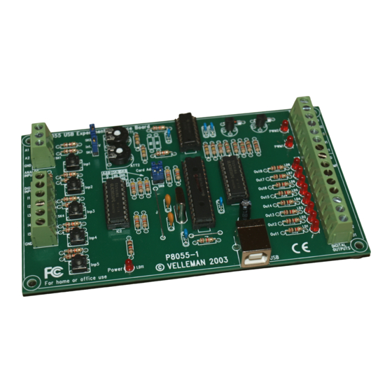
- Page 3 Features Features: 5 Digital inputs (0= ground, 1= open). On board test buttons provided. 2 Analog inputs with attenuation and amplification option. Internal test +5V provided. 8 Digital open collector output switches (max 50V/100mA). On board LED indication. 2 Analog outputs 0 to 5V, output resistance 1K5.
- Page 4 Assembly hints 1. Assembly (Skipping this can lead to troubles ! ) Ok, so we have your attention. These hints will help you to make this project successful. Read them carefully. 1.1 Make sure you have the right tools: • A good quality soldering iron (25-40W) with a small tip.
- Page 5 Assembly hints 1.3 Soldering Hints : 1- Mount the component against the PCB surface and carefully solder the leads 2- Make sure the solder joints are cone-shaped and shiny 3- Trim excess leads as close as possible to the solder joint REMOVE THEM FROM THE TAPE ONE AT A TIME ! AXIAL COMPONENTS ARE TAPED IN THE COR- RECT MOUNTING SEQUENCE !
- Page 6 Construction 3. Resistors R24 : 10K (1 - 0 - 3 - B) 1. Jumper R25 : 10K (1 - 0 - 3 - B) R26 : 10K (1 - 0 - 3 - B) R... R27 : 1K (1 - 0 - 2 - B) R28 : 47K (4 - 7 - 3 - B) R29 : 47K...
- Page 7 Construction 4. Ceramic Capacitors 6. Push buttons 8. Capacitors. C... C... SW... C1 : 100nF (104, 0.1, u1) C2 : 100nF (104, 0.1, u1) C6 : 220nF/50V~ C3 : 100nF (104, 0.1, u1) C4 : 33pF (33) C5 : 33pF (33) 9.
- Page 8 Construction 10. Transistors 12. Electrolytic capacitor. 14. Header Watch the polarity ! C8 : 4,7µF/50V C... T1 : BC337 T2 : BC337 SK2 : 2P 13. Quartz crystal SK3 : 2P 11. USB connector SK5 : 2P X... SK6 : 2P 15.
- Page 9 Construction 16. IC’s. Watch the position of the notch! IC1 : TLV274IN IC2 : ULN2803 IC3 : VK8055 (Programmed PIC16C745-IP) PIN 1 IC4 : ULN2803 SK4 : 2 x 3P SK8 : 5 x 3P...
-
Page 10: Gain Factor
Gain factor 17. GAIN FACTOR The analogue inputs A1 and A2 have a standard range of 0 ~ +5Vdc. To use them externally, remove the jumper caps on SK2 and SK3. The internal 5V voltage source can only be used for testing purposes. When the input voltage is too low you can amplify it x4 / x15. -
Page 11: Rubber Feet
Rubber feet 18. Rubber feet Mount the rubber feet on the solder side of the PCB, see fig 1.0. Fig. 1.0... - Page 12 Connection / settings 19. Connection / settings...
- Page 13 Connection / settings 5 digital inputs (e.g. push button, switch, relay contact, ...). Input is generally "high" (1), connection to GND makes the input "low" (0) Analogue inputs (e.g. temperature sensor, potentiometer, ...) 0 ... +5VDC MAX! If the jumper is mounted, then you can use the internal voltage and adjust it using RV2/RV1. If the jumper is not mounted you must use the external voltage A2/A1.
-
Page 14: Digital Outputs
Connection / settings Select the correct address in the test program DIGITAL OUTPUTS : 8 open collector contacts, to be connected with suitable inputs. These exits function as ‘dry contact points’: you need an external voltage to control a component such as a LED or a relay switch. - Page 15 • Start “Setup.exe”, this software is located at the folder K8055 from the Velleman Software CD. If the necessary software is not included or if you want to check for updates, you can always download it for free from our Velle- man Website www.velleman.be...
-
Page 16: Test Procedure
LED LD3 'Power' lights up if the connection has been executed properly. After startup LD8 (output 8) will flash momentarily to indicate that the circuit works as it should. Start the program 'K8055_Demo.exe'. Next press the 'connect' button to connect the K8055 with the computer. - Page 17 Test procedure The message "Card x connected" is displayed if the connection is successful, see fig 3.0. FIG 3.0 You can now simulate the inputs via push buttons Inp1 through Inp5. The matching check box remains ticked off as long as you keep one of the push buttons pressed down. Always tick off the check box for the matching output if you wish to test a digital output.
- Page 18 Test procedure Counter 1 & 2 are hardware integrated 16-bit counters, they are triggered by INP1 & INP2. You can test the counter with push buttons Inp1 and Inp2 : the counter adds 1every time one of these two buttons is pressed.
-
Page 19: Connection Scheme
Connection scheme 22. CONNECTION SCHEME ANALOG VOLTAGE 0 ...5V RVx : FOR EXPERIMENTAL USE mount SK2 & SK3 when using RV1,2 "1" "0" To external electronics analog output 0 ... 5V 220V P8055-1 VELLEMAN 2003 EXTERNAL ! DC voltage 5 ... 30V DC Adapter (ex. - Page 20 23. PCB...
- Page 21 Schematic diagram 24. Schematic diagram.
- Page 22 This device complies with Part 15 of the FCC Rules provided the enclosed instructions are followed to the letter. Use of the device is subject to the following conditions: (1) this device must not cause harmful interference and (2) the operation of this device should not be influenced by unwanted interfer- ence.
- Page 24 VELLEMAN Components NV Legen Heirweg 33 9890 Gavere Belgium Europe www.velleman.be www.velleman-kit.com Modifications and typographical errors reserved © Velleman Components nv. H8055IP - 2005 - ED1 (rev 3.0) 5 4 1 0 3 2 9 2 9 2 0 6 5...
Need help?
Do you have a question about the K8055 and is the answer not in the manual?
Questions and answers