Table of Contents
Advertisement
Quick Links
Advertisement
Table of Contents

Related Manuals for Clevo NJ70PU


Summary of Contents for Clevo NJ70PU
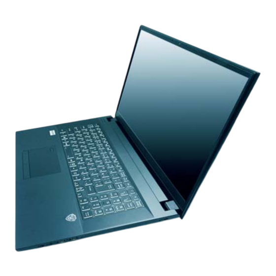
- Page 1 NJ70PU...
- Page 3 Preface Notebook Computer NJ70PU Service Manual...
- Page 4 Preface Notice The company reserves the right to revise this publication or to change its contents without notice. Information contained herein is for reference only and does not constitute a commitment on the part of the manufacturer or any subsequent ven- dor.
- Page 5 This manual is intended for service personnel who have completed sufficient training to undertake the maintenance and inspection of personal computers. It is organized to allow you to look up basic information for servicing and/or upgrading components of the NJ70PU se- ries notebook PC.
- Page 6 Preface IMPORTANT SAFETY INSTRUCTIONS Follow basic safety precautions, including those listed below, to reduce the risk of fire, electric shock and injury to per- sons when using any electrical equipment: 1. Do not use this product near water, for example near a bath tub, wash bowl, kitchen sink or laundry tub, in a wet basement or near a swimming pool.
- Page 7 Preface Instructions for Care and Operation The notebook computer is quite rugged, but it can be damaged. To prevent this, follow these suggestions: Don’t drop it, or expose it to shock. If the computer falls, the case and the components could be damaged. Do not expose the computer Do not place it on an unstable Do not place anything heavy...
- Page 8 Preface Avoid interference. Keep the computer away from high capacity transformers, electric motors, and other strong mag- netic fields. These can hinder proper performance and damage your data. Take care when using peripheral devices. Use only approved brands of Unplug the power cord before peripherals.
- Page 9 Preface Battery Precautions • Only use batteries designed for this computer. The wrong battery type may explode, leak or damage the computer. • Do not continue to use a battery that has been dropped, or that appears damaged (e.g. bent or twisted) in any way. Even if the computer continues to work with a damaged battery in place, it may cause circuit damage, which may possibly result in fire.
- Page 10 Preface Related Documents You may also need to consult the following manual for additional information: User’s Manual on CD/DVD This describes the notebook PC’s features and the procedures for operating the computer and its ROM-based setup pro- gram. It also describes the installation and operation of the utility programs provided with the notebook PC. System Startup 1.
-
Page 11: Table Of Contents
Preface Contents Introduction ..........1-1 Top ....................A-3 Bottom ................... A-4 Overview ..................1-1 LCD ....................A-5 Specifications ..................1-2 DVD ....................A-6 External Locator - Top View with LCD Panel Open ......1-4 HDD ....................A-7 External Locator - Front & Right Side Views .........1-5 MB .................... - Page 12 Preface M Key PCIE SSD ................. B-25 USB, HDD, ODD ................. B-26 LAN I219V .................. B-27 Card Reader OZ711 ..............B-28 M.2 Card (3G/LTE) ..............B-29 M.2 Card (BT/WLAN) ..............B-30 Audio Codec ................. B-31 CONN FAN, TP, CCD, LED ............B-32 KBC ITE IT5570 ................
-
Page 13: Introduction
Chapter 1: Introduction Overview This manual covers the information you need to service or upgrade the NJ70PU series notebook computer. Information about operating the computer (e.g. getting started, and the Setup utility) is in the User’s Manual. Information about dri- vers (e.g. -
Page 14: Specifications
Introduction Specifications Processor Options Video Adapter Intel® Core™ i7 Processor Intel Iris Xe Graphics ( i7-1255U, i5-1235U) i7-1255U (1.70GHz) HDR Support Intel® Core™ i5 Processor Rec. 2020 (Wide Color Gamut) i5-1235U (1.30GHz) Microsoft DirectX® 12 Compatible Latest Specification Information Intel®... - Page 15 Introduction Card Reader Power Embedded Multi-In-1 Card Reader Full Range AC/DC Adapter MMC (MultiMedia Card) / RS MMC AC Input: 100 - 240V, 50 - 60Hz DC Output: 19V, 2.37A (45W) SD (Secure Digital) / Mini SD / SDHC/ SDXC Removable 4 Cell Smart Lithium-Ion Battery Pack, 32WH Interface (Factory Option) Removable 4 Cell Smart Lithium-Ion Battery...
-
Page 16: External Locator - Top View With Lcd Panel Open
Introduction External Locator - Top View with LCD Panel Open Figure 1 Top View 1. Webcam 2. *Camera LED *When the PC camera is in use, the LED will be illuminated in white. 3. Built-In Array Microphone 4. Display 5. Power Button 6. -
Page 17: External Locator - Front & Right Side Views
Introduction External Locator - Front & Right Side Views Figure 2 Front View 1. LED Indicators 2. Multi-in-1 Card Reader FRONT VIEW Figure 3 Right Side View 1. 2-In-1 Audio Jack (Headphone and Microphone) 2. Microphone-In Jack RIGHT SIDE VIEW 3. -
Page 18: External Locator - Left Side & Rear View
Introduction External Locator - Left Side & Rear View Figure 4 Left Side View 1. DC-In Jack 2. RJ-45 LAN Jack 3. External Monitor LEFT SIDE VIEW Port 4. USB 3.2 Gen 2 Type-C Port with DisplayPort and Power Delivery 5. -
Page 19: External Locator - Bottom View
Introduction External Locator - Bottom View Figure 6 Bottom View 1. Battery 2. Vent 3. Speakers 4. Multi-in-1 Card Reader Overheating To prevent your com- puter from overhea- ting, make sure no- thing blocks any vent while the computer is in use. -
Page 20: Mainboard Overview - Top (Key Parts)
Introduction Mainboard Overview - Top (Key Parts) Figure 7 Mainboard Top Key Parts 1 - 8 Mainboard Overview - Top (Key Parts) -
Page 21: Mainboard Overview - Bottom (Key Parts)
Introduction Mainboard Overview - Bottom (Key Parts) Figure 8 Mainboard Bottom Key Parts 1. CPU 2. Memory Slots DDR4 SO-DIMM 3. KBC-ITE IT5570 4. CMOS Battery Mainboard Overview - Bottom (Key Parts) 1 - 9... -
Page 22: Mainboard Overview - Top (Connectors)
Introduction Mainboard Overview - Top (Connectors) Figure 9 Mainboard Top Connectors 1. DC-In Jack 2. RJ-45 LAN Jack 3. External Monitor Port 4. USB 3.2 Gen 2 Type-C Port with Power Delivery 5. HDMI-Out Port 6. USB 3.2 Gen 1 Type-A Port (Factory Option) Powered USB 3.2... -
Page 23: Mainboard Overview - Bottom (Connectors)
Introduction Mainboard Overview - Bottom (Connectors) Figure 10 Mainboard Bottom Connectors 1. ODD Connector 2. HDD Connector 3. Multi-in-1 Card Reader 4. M.2 Card Connector 5. Fan Connector 6. LCD Cable Connector 7. WLAN Connector 8. LTE Connector 9. SIM Card Reader 10. - Page 24 Introduction 1 - 12...
-
Page 25: Disassembly
Chapter 2: Disassembly Overview This chapter provides step-by-step instructions for disassembling the NJ70PU series notebook’s parts and subsystems. When it comes to reassembly, reverse the procedures (unless otherwise indicated). We suggest you completely review any procedure before you take the computer apart. -
Page 26: Maintenance Tools
Disassembly NOTE: All disassembly procedures assume that the system is turned OFF, and disconnected from any power supply (the battery is removed too). Maintenance Tools The following tools are recommended when working on the notebook PC: • M3 Philips-head screwdriver •... -
Page 27: Maintenance Precautions
Disassembly Maintenance Precautions The following precautions are a reminder. To avoid personal injury or damage to the computer while performing a removal and/or replacement job, take the following precautions: Power Safety Don't drop it. Perform your repairs and/or upgrades on a stable surface. If the computer falls, the case and other components Warning could be damaged. -
Page 28: Disassembly Steps
Disassembly Disassembly Steps The following table lists the disassembly steps, and on which page to find the related information. PLEASE PERFORM THE DISASSEMBLY STEPS IN THE ORDER INDICATED. To remove the Battery: To remove the 4G Module: 1. Remove the battery page 2 - 5 1. -
Page 29: Removing The Battery
Disassembly Removing the Battery Figure 1 Battery Removal 1. Turn off the computer, turn it over. 2. Slide the latch in the direction of the arrow (Figure 1a a. Slide the latch and hold it 3. Slide the latch in the direction of the arrow, and hold it in place (Figure 1a in place. -
Page 30: Removing The Hard Disk Drive
Disassembly Removing the Hard Disk Drive Figure 2 The hard disk drive can be taken out to accommodate other 2.5" serial (SATA) hard disk drives with a height of 7.0mm HDD Assembly (h). Follow your operating system’s installation instructions, and install all necessary drivers and utilities (as outlined in Removal Chapter 4 of the User’s Manual) when setting up a new hard disk. - Page 31 Disassembly 5. Remove screws from the HDD assembly (Figure 3d). Figure 3 6. Slightly lift and pull the hard disk assembly up using the tab (Figure 3e HDD Assembly 7. Lift the hard disk assembly out of the bay (Figure 3f Removal (cont’d.) 8.
-
Page 32: Removing The System Memory (Ram)
Disassembly Removing the System Memory (RAM) Figure 4 RAM Module The computer has two memory sockets for 260 pin Small Outline Dual In-line Memory Modules (SO-DIMM) supporting Removal DDR4 3200MHz. The main memory can be expanded up to 64GB. The total memory size is automatically detected by the POST routine once you turn on your computer. - Page 33 Disassembly 5. Pull the latches to release the second module if necessary. 6. Insert a new module holding it at about a 30° angle and fit the connectors firmly into the memory slot. 7. The module will only fit one way as defined by its pin alignment. Make sure the module is seated as far into the slot as it will go.
-
Page 34: Removing The Keyboard
Disassembly Removing the Keyboard Figure 5 1. Turn off the computer, turn it over to remove the battery (page 2 - 10) and component cover (page 2 - Keyboard Removal 2. Locate the release points from the open bottom case (Figure 5a). -
Page 35: Removing The Optical (Cd/Dvd) Device
Disassembly Removing the Optical (CD/DVD) Device Figure 6 Optical Device 1. Turn off the computer, remove the battery (page 2 - 5), and bottom case (page 2 - Removal 2. Remove the screw and push the optical device out of the bay in the direction of the arrow (Figure 6a 3. -
Page 36: Removing The Wireless Lan Module
Disassembly Removing the Wireless LAN Module Figure 7 Wireless LAN 1. Turn off the computer, turn it over to remove the keyboard (page 2 - 10) and battery (page 2 - Module Removal 2. The Wireless LAN module will be visible at point on the mainboard (Figure 7a). -
Page 37: Wireless Lan, And Combo Module Cables
Disassembly Wireless LAN, and Combo Module Cables Note that the cables for connecting to the antennae on WLAN, WLAN & Bluetooth Combo modules are not labelled. The cables/covers (each cable will have either a black or transparent cable cover) are color coded for identification as outlined in the table below. -
Page 38: Removing The 4G Module
Disassembly Removing the 4G Module Figure 8 4G Module Removal 1. Turn off the computer, turn it over to remove the keyboard (page 2 - 10) and battery (page 2 - 2. The module will be visible at point on the mainboard (Figure 7a). -
Page 39: Removing The M.2 Ssd Module
Disassembly Removing the M.2 SSD Module Figure 9 M.2 SSD Module 1. Turn off the computer, turn it over to remove the keyboard (page 2 - 10) and battery (page 2 - Removal 2. The M.2 SSD module will be visible at point on the mainboard (Figure 9a). -
Page 40: Removing The Ccd
Disassembly Removing the CCD Figure 10 CCD Removal 1. Turn off the computer, turn it over to remove the keyboard (page 2 - 10) and battery (page 2 - 2. Run your fingers around the inner frame of the LCD panel at the points as indicated by the arrows (Figure a. - Page 41 Disassembly 4. Disconnect the cable (Figure 11f). Figure 11 5. Remove the CCD module (Figure 11g). CCD Removal 6. Reverse the process to install a new CCD module. (cont’d.) c. Disconnect the cable. d. Remove the CCD mod- ule. 6.
- Page 42 Disassembly 2 - 18...
-
Page 43: Part Lists
Appendix A: Part Lists This appendix breaks down the NJ70PU series notebook’s construction into a series of illustrations. The component part numbers are indicated in the tables opposite the drawings. Note: This section indicates the manufacturer’s part numbers. Your organization may use a different system, so be sure to cross-check any relevant documentation. -
Page 44: Part List Illustration Location
Part List Illustration Location The following table indicates where to find the appropriate part list illustration. Table A - 1 Part List Illustration Part Location page A - 3 page A - 4 Bottom page A - 5 page A - 6 page A - 7 page A - 8 A - 2... -
Page 45: Top
Figure A - 1 Top A - 3... -
Page 46: Bottom
Bottom Figure A - 2 Bottom A - 4 Bottom... -
Page 47: Lcd
Figure A - 3 LCD A - 5... -
Page 48: Dvd
Figure A - 4 A - 6 DVD... -
Page 49: Hdd
Figure A - 5 HDD A - 7... - Page 50 Figure A - 6 A - 8 MB...
-
Page 51: Schematic Diagrams
Schematic Diagrams Appendix B: Schematic Diagrams This appendix has circuit diagrams of the NJ70PU notebook’s PCB’s. The following table indicates where to find the appropriate schematic diagram. Diagram - Page Diagram - Page Diagram - Page Table B - 1... - Page 52 Schematic Diagrams System Block Diagram NJ50PU Alder Lake P System Block Diagram NJ50/70 AUDIO BOARD VDD3,VDD5 SHEET 33 6-71-NJ5P8-D01 SHEET 43.44 DD_ON#, SUSB, 5V, 5VS, 1.8V NJ50 CLICK BOARD DDR4 IT6516 3.3V, 3.3VS, 3.3VA TCP0 6-71-NJ5P2-D01 SHEET 45 SHEET 34 SO-DIMM_A_0 DP TO VGA <10"...
-
Page 53: Processor 10/13
Schematic Diagrams Processor 1/13 U48B INS116297625 BMAP_REV = 0.52 M_A_DQ[63:0] DDR4(IL) / DDR4(NIL) / DDR5(NIL) / LP4x-LP5(NIL) M_A_DQ63 DH58 CD49 DDR0_DQ_0_7/DDR0_DQ_0_7/DDR0_DQ_0_7/DDR0_DQ_0_7 DDR0_CLK_P_1/DDR3_CLK_P/DDR3_CLK_P/DDR3_CLK_P/DDR1_CLK_P_1 M_A_CLK_DDR1 M_A_DQ62 DG57 CD48 DDR0_DQ_0_6/DDR0_DQ_0_6/DDR0_DQ_0_6/DDR0_DQ_0_6 DDR0_CLK_N_1/DDR3_CLK_N/DDR3_CLK_N/DDR3_CLK_N/DDR1_CLK_N_1 M_A_DQ61 M_A_CLK_DDR#1 DH56 CH61 DDR0_DQ_0_5/DDR0_DQ_0_5/DDR0_DQ_0_5/DDR0_DQ_0_5 NC/DDR2_CLK_P/DDR2_CLK_P/DDR2_CLK_P/DDR1_CLK_P_0 M_A_DQ60 DG60 CF61 DDR0_DQ_0_4/DDR0_DQ_0_4/DDR0_DQ_0_4/DDR0_DQ_0_4 NC/DDR2_CLK_N/DDR2_CLK_N/DDR2_CLK_N/DDR1_CLK_N_0 M_A_DQ59 DL60 CN49 DDR0_DQ_0_3/DDR0_DQ_0_3/DDR0_DQ_0_3/DDR0_DQ_0_3... - Page 54 Schematic Diagrams Processor 2/13 U48C INS116299312 BMAP_REV = 0.52 M_B_DQ[63:0] DDR4 / LP4x / LP5_ascend / LP5_descend / DDR5 M_B_DQ63 BB58 DDR0_DQ_4_7/DDR1_DQ_0_7/DDR2_DQ_0_7/DDR4_DQ_0_7 DDR1_CLK_P_1/DDR7_CLK_P/DDR7_CLK_P/DDR7_CLK_P/DDR3_CLK_P_1 M_B_CLK_DDR1 M_B_DQ62 BA57 DDR0_DQ_4_6/DDR1_DQ_0_6/DDR2_DQ_0_6/DDR4_DQ_0_6 DDR1_CLK_N_1/DDR7_CLK_N/DDR7_CLK_N/DDR7_CLK_N/DDR3_CLK_N_1 M_B_CLK_DDR#1 M_B_DQ61 BB56 AB61 DDR0_DQ_4_5/DDR1_DQ_0_5/DDR2_DQ_0_5/DDR4_DQ_0_5 NC/DDR6_CLK_P/DDR6_CLK_P/DDR6_CLK_P/DDR3_CLK_P_0 M_B_DQ60 BA60 DDR0_DQ_4_4/DDR1_DQ_0_4/DDR2_DQ_0_4/DDR4_DQ_0_4 NC/DDR6_CLK_N/DDR6_CLK_N/DDR6_CLK_N/DDR3_CLK_N_0 M_B_DQ59 BE60 AG49 DDR0_DQ_4_3/DDR1_DQ_0_3/DDR2_DQ_0_3/DDR4_DQ_0_3 NC/DDR5_CLK_P/DDR5_CLK_P/DDR5_CLK_P/DDR2_CLK_P_1...
-
Page 55: Processor 11/13
Schematic Diagrams Processor 3/13 U48A INS116300728 BMAP_REV = 0.52 EDP_TXP_3 DDIA_TXP_3 TCP0_TXRX_P1 DDIA_TXN_3 TCP0_TXRX_N1 EDP_TXN_3 EDP_TXP_2 DDIA_TXP_2 TCP0_TXRX_P0 VGA_1P EDP_TXN_2 DDIA_TXN_2 TCP0_TXRX_N0 VGA_1N EDP_TXP_1 DDIA_TXP_1 TCP0_TX_P1 VGA PORT eDP PANEL EDP_TXN_1 DDIA_TXN_1 TCP0_TX_N1 VGA_0P EDP_TXP_0 DDIA_TXP_0 TCP0_TX_P0 DIFF=85ohm DDIA_TXN_0 TCP0_TX_N0 VGA_0N EDP_TXN_0 TCP0_AUX_P... - Page 56 Schematic Diagrams Processor 4/13 ADL-P I2C, ISH, AUDIO For BIOS Debug VDD3 UART0_RX R662 *10K_04 R667 *0_06 UART0_TX R666 *10K_04 U48F REWORK INS116301360 BMAP_REV = 0.52 UART0_TX EN48 EY28 GPP_H11/UART0_TXD/M2_SKT2_CFG1 GPP_D14/ISH_UART0_TXD/I2C4B_SCL SSD1_PWR_EN UART0_RX EN46 EV28 GPP_H10/UART0_RXD/M2_SKT2_CFG0 GPP_D13/ISH_UART0_RXD/I2C4B_SDA WLAN_WAKEUP#_R GPP_H13 EL41 EY36 GPP_H13/I2C7_SCL/UART0_CTS#/M2_SKT2_CFG3/ISH_GP7B/DEVSLP1B GPP_D16/ISH_UART0_CTS#/I2C7B_SCL...
-
Page 57: Processor 12/13
Schematic Diagrams Processor 5/13 ADL-P PEG PCIE Zdiff=85Ω 2.5" ~ 8 " 3.3VS U48H INS116302031 WLAN_CLKREQ# R656 10K_04 BMAP_REV = 0.52 R222 10K_04 CARD_CLKREQ# PCIE4_TXP3_SSD PCIEX4_A_TX_P_3 PCIEX8_TX_P_7 PCIEX4_A_TX_N_3 PCIEX8_TX_N_7 GLAN_CLKREQ# PCIE4_TXN3_SSD R655 *10K_04 PCIE4_RXP3_SSD PCIEX4_A_RX_P_3 PCIEX8_TX_P_6 SSD1_CLKREQ# PCIE4_RXN3_SSD PCIEX4_A_RX_N_3 PCIEX8_TX_N_6 R663 10K_04 PCIEX8_TX_P_5... - Page 58 Schematic Diagrams Processor 6/13 U48I ADL-P PCIE, USB3, USB2 INS116302999 BMAP_REV = 0.52 DY10 SATA_TXP1_ODD PCIE12_TXP/SATA1_TXP USB2P_10 USB_PP10_BT BLUETOOTH DY11 DIFF=85ohm SATA_TXN1_ODD PCIE12_TXN/SATA1_TXN USB2N_10 USB_PN10_BT SATA_RXP1_ODD PCIE12_RXP/SATA1_RXP EL18 SATA_RXN1_ODD PCIE12_RXN/SATA1RXN USB2P_9 EN18 USB2N_9 EB10 SATA_TXP0_HDD PCIE11_TXP/SATA0_TXP EB11 PCIE11_TXN/SATA0_TXN USB2P_8 SATA_TXN0_HDD SATA_RXP0_HDD PCIE11_RXP/SATA0_RXP USB2N_8...
-
Page 59: Processor 13/13
Schematic Diagrams Processor 7/13 ADL-P SPI,ESPI, THC, MLINK,SMLINK,SMBUS 3.3VA TO TPM SML0_DATA R693 499_1%_04 SPI_SCLK_R SML0_CLK R509 56_1%_04 R694 499_1%_04 TPM_SPI_CLK SMB_DATA R314 1K_04 SPI_SO_R R505 56_1%_04 SMB_CLK R315 1K_04 TPM_SPI_MISO GPP_C6 R670 1K_04 SPI_SI_R GPP_C7 R512 56_1%_04 R246 1K_04 TPM_SPI_MOSI 0_04 SPI0_CS2#... - Page 60 Schematic Diagrams Processor 8/13 ADL-P RSVD ADL-P CSI, CNV U48J To M.2 INS116304474 BMAP_REV = 0.52 DIFF=85ohm, L<10" AD41 FC46 CSI_D_DP_1/CSI_C_DP_2 CNV_WT_D1P CNVI_WT_D1P AB41 FA46 M.2 PCIE CSI_D_DN_1/CSI_C_DN_2 CNV_WT_D1N CNVI_WT_D1N AG41 EV43 CSI_D_DP_0/CSI_C_DP_3 CNV_WT_D0P U48T CNVI_WT_D0P AF41 EY43 (PCIEX4 A) CSI_D_DN_0/CSI_C_DN_3 CNV_WT_D0N CNVI_WT_D0N...
- Page 61 Schematic Diagrams Processor 9/13 ADL-P CPU JTAG, PCH JTAG, MISC PU/PD for JTAG signals VCCST H_THERMTRIP# R237 1K_04 PCH_JTAG_TDI R179 51_04 PCH_JTAG_TMS R175 51_04 PCH_JTAG_TDO R189 100_04 CPU_JTAG_TDO R187 100_04 XDP_PREQ# R171 *51_04 EAR# R217 1K_04 CPU_JTAG_TCLK R173 51_04 PCH_JTAG_TRST R174 *51_04 U48V...
- Page 62 Schematic Diagrams Processor 10/13 ADL-P SYSTEM POWER MANAGEMENT 3.3VS U48L SYS_RESET# R234 10K_04 INS116306042 BMAP_REV = 0.52 3.3VA PWR_BTN# EN53 EM61 SLP_SUS# GPD3/PWRBTN# 32,34,36 SLP_SUS# PWR_BTN# EM56 PM_BATLOW# GPD0/BATLOW# PM_BATLOW# PCIE_WAKE# SLP_S5# AC_PRESENT R692 8.2K_04 EG60 EJ59 GPD10/SLP_S5# GPD1/ACPRESENT AC_PRESENT SUSC#_PCH EP56 GPD5/SLP_S4#...
- Page 63 Schematic Diagrams Processor 11/13 ADL-P CPU POWER PRIMARY SIDE U48M U48O 47uF_6.3v_X5R_06 x 5 VCORE VCORE VDDQ VCCGT INS116307569 INS116307281 VCORE BMAP_REV = 0.52 BMAP_REV = 0.52 2.57A BA44 AD61 CP44 VCCCORE_1 VCCCORE_51 VDD2_1 VCCGT_1 BB43 AG61 CR45 VCCCORE_2 VCCCORE_52 VDD2_2 VCCGT_2 C454...
- Page 64 Schematic Diagrams Processor 12/13 PRIMARY SIDE ADL-P PCH POWER 47u_6.3V_X5R_06 VCCIN_AUX U48N 1.8VA VCCIN_AUX INS116309120 BMAP_REV = 0.52 1.533A AL20 DW20 VCCIN_AUX_1 VCCPRIM_1P8_1 AL32 DW22 VCCIN_AUX_2 VCCPRIM_1P8_2 AN20 DW27 VCCIN_AUX_3 VCCPRIM_1P8_3 AN22 DW30 VCCIN_AUX_4 VCCPRIM_1P8_4 AN30 DY21 VCCIN_AUX_5 VCCPRIM_1P8_5 AN32 DY23 VCCIN_AUX_6 VCCPRIM_1P8_6...
- Page 65 Schematic Diagrams Processor 13/13 ADL-P GND U48P U48Q U48R U48S INS116313805 INS116312893 INS116314262 INS116313351 BMAP_REV = 0.52 BMAP_REV = 0.52 BMAP_REV = 0.52 BMAP_REV = 0.52 NCTF AL15 BF58 CD58 DC47 ED58 NCTF AL17 CE51 DC54 BG12 CE55 ED60 AL22 DC57 BG44 CF47...
-
Page 66: Ddr4 So_Dimm_A
Schematic Diagrams DDR4 SO_DIMM_A SO-DIMM A VDDQ VDDQ_VTT J_DIMMA1A J_DIMMA1B M_A_DQ[63:0] M_A_DQ7 M_A_CLK_DDR0 CK0_T VDD19 M_A_DQ2 2.5V M_A_CLK_DDR#0 CK0_C VDD18 M_A_DQ3 M_A_CLK_DDR1 CK1_T M_A_DQ0 VDD17 M_A_CLK_DDR#1 CK1_C VDD16 VPP2 M_A_DQ6 VDD15 VPP1 M_A_DQ5 M_A_CKE0 CKE0 VDD14 M_A_DQ4 M_A_CKE1 CKE1 M_A_DQ1 VDD13 3.3VS VDD12... -
Page 67: Ddr4 So_Dimm_B
Schematic Diagrams DDR4 SO_DIMM_B SO-DIMM B VDDQ_VTT VDDQ J_DIMMB1A J_DIMMB1B M_B_DQ[63:0] M_B_DQ23 M_B_CLK_DDR0 CK0_T M_B_DQ20 VDD19 2.5V M_B_CLK_DDR#0 CK0_C VDD18 M_B_DQ16 M_B_CLK_DDR1 CK1_T VDD17 M_B_DQ19 M_B_CLK_DDR#1 CK1_C VDD16 VPP2 M_B_DQ21 M_B_DQ22 VDD15 VPP1 M_B_CKE0 CKE0 M_B_DQ17 VDD14 M_B_CKE1 CKE1 VDD13 M_B_DQ18 3.3VS VDD12... -
Page 68: Panel, Inverter
Schematic Diagrams Panel, Inverter PANEL CONNECTOR PLVDD PANEL POWER EMI change eDP panel J_LCD1 1u_6.3V_X5R_04 0.1u_50V_X5R_04 Default Short *OPEN_2A VLED C299 0.1u_10V_X5R_04 EDP_TXN_0 *MTP3403N3 >120 mil C300 0.1u_10V_X5R_04 EDP_TXP_0 C301 0.1u_10V_X5R_04 EDP_TXN_1 C310 3.3V C302 0.1u_10V_X5R_04 EDP_TXP_1 *0.22u_25V_X7R_06 GND1 C285 C303 0.1u_10V_X5R_04 EDP_TXN_2... -
Page 69: Hdmi
Schematic Diagrams HDMI HDMI CONNECTOR ( W/O LEVELSHIFT) HDMI_5VS C144 J_HDMI1 VOUT *10u_6.3V_X5R_04 16-A2820-1A03-0 C162 C143 C142 APL3517A HDMI_HPD-C-R HOT PLUG DETECT DDC/CEC GND HDMI_SDA-C-R HDMI_SCL-C-R BY PLATFROM RESERVED HDMI_CEC BY PLATFROM TMDS_CLOCK#J TMDS CLOCK- R366 470_04 CLK SHIELD R352 470_04 TMDS_CLOCKJ TMDS_DATA0#... -
Page 70: Dp To Vga It6516
Schematic Diagrams DP to VGA IT6516 RX_AVCC IVDDO HCB1005KF-121T20 C344 3.3VS 3.3VS IVDDO RX_IVDD C361 C345 10u_6.3V_X5R_04 0.1u_10V_X7R_04 10u_6.3V_X5R_04 R576 4.7K_04 VGA_HPD C361 is close to pin25 C333 0.1u_10V_X7R_04 VGA_0P RX0P RSVD C341 0.1u_10V_X7R_04 VGA_0N RX0N RX_IVDD C339 0.1u_10V_X7R_04 IVDDO VGA_1P RX1P C340... -
Page 71: Rgb Kb
Schematic Diagrams RGB KB NJ50 RGB KB Only VDD3 RGBKB_PWR J_KBLED1 Follow , 0606 R619 100K_04 NJ50 NJ50 1K_04 R621 RGBKB-DET# KBZONE_B R620 100_04 NJ50 KBZONE_R KBZONE_G R603 0_06 RGBKBSW_R KBZONE_R FP0501H-080BN fp225h-008gxxxm_r P/N = 6-20-94K30-108 RGBKB-DET# R713 0_02 SM3422KTDSH LEDKB_DET# 32 EC_PWM_LEDKB_R NJ50... -
Page 72: Tpm, Pw Button, Lid Sw, Led
Schematic Diagrams TPM, PW Button, LID SW, LED TPM_3.3V POWER BUTTON / LED GPIO H: W / TPM ( R461) 10K_04 L: W/O TPM ( R462) 3.3VS POWER TPM_DET 11 SWITCH R475 100K_04 VDD3 TPM_3.3V W/O TPM D02,Hank,Power LED 330_04 POWER ON LED 3.3VA *0_04... -
Page 73: Type-C
Schematic Diagrams Type-C 3.3V TOTAL 23mA VDD5 Tim, 0606 3.3V C389 HCB1005KF-121T20 VDD33 1u_6.3V_X5R_02 PS8802_3.3V PS8802_3.3V VOUT C430 C431 R152 C367 DD_ON 0.1u_6.3V_X5R_02 4.7u_6.3V_X5R_04 R162 10K_04 3.48K_1%_04 AP2204K-ADJTRG1 C397 1.14V~1.26V TOTAL 393mA HCB1005KF-121T20 R161 VDD_DM_D1 VDD_DM_D1 1.2V 1.91K_1%_04 USB3.1 GEN2 EPAD Swap, 0606 0.01u_16V_X7R_04... -
Page 74: Pd Controller It8851
Schematic Diagrams PD Controller IT8851 Table 6-1. I2C0 Slave ID Decode Tim Add, 0615 PD_3.3V 3.3V R128 10K_04 *SS14WS PS8802_3.3V Slave ID SS14WS USBVCC3.1_1 VBUS_LDO3.3V 100 MIL SS14WS 7'h40 C359 C351 C352 0.1u_6.3V_X5R_02 1u_6.3V_X5R_02 10u_6.3V_X5R_04 7'h42 10u_6.3V_X5R_04 1u_25V_X5R_04 1u_25V_X5R_04 FA7616EA5R 7'h50 SOURCE_CTRL 7'h52... -
Page 75: M Key Pcie Ssd
Schematic Diagrams M Key PCIE SSD NGFF_M (M2) SSD (PCIE 4X) Port2 3.3VS R349 SSD1_3.3VS J_SSD1 C216 C228 C158 100K_04 EMI change GND13 GND12 3.3V8 *PESD5V0R1BSF GND11 3.3V7 PEDET(NC-PCIe/GND-SATA) 3.3V6 NC18 SUSCLK(32Khz)(O) M KEY FOR OPTANE SUPPORT 10u_6.3V_X5R_06 -->22u GND10 NC17 CLK_PCIE_SSD1 REFCLKP... -
Page 76: Usb, Hdd, Odd
Schematic Diagrams USB, HDD, ODD USB 3.0 port (CHARGER) Smart CDP pin8 pin4 Function C509 22u_6.3V_X5R_06 USB3.0 Max Trace length DCP autodetect with Follow Design Guide C510 22u_6.3V_X5R_06 mouse/keyboard wake up USBVCC_CH S0 Charging with SDP CLOSE TO CONNECTOR Julie SWAP J_USB3_1 USB3_TXP1_USBA USB3_1TXPC... -
Page 77: Lan I219V
Schematic Diagrams LAN I219V GIGA LAN (INTEL LAN I219) LAN i219 VDD3 The 10Kohm pull-up resistor of CLK_REQ_N is required to either 3.3V Suspend (5, 6, 7) or Core (2) rail, depending on the power well of PCH's input PCIECLKRQx# buffer. -
Page 78: Card Reader Oz711
Schematic Diagrams Card Reader OZ711 CARD READER 3.3VS OZ711 /SD NJ50CU J_CARD-REV1 CARD_RTD3_RST# CARD_RTD3_RST#_R SD_D3_R SD_CMD_R CD/DAT3 BUF_PLT_RST# 11,21,24,26,29,32 *74AHC1G08GW VSS1 VCC_CARD SD_CLK_R *MTH8_0D2_8 C401 SD_D0_R VSS2 NJ50 SD_D1_R DAT0 R347 0_04 0.1u_6.3V_X5R_02 SD_D2_R DAT1 DAT2 MS_BS/SD_WP#_R VDD3 3V3AUX SD_CD#_R WRITE PROTECT 3V3AUX VCC_CARD... -
Page 79: Card (3G/Lte
Schematic Diagrams M.2 Card (3G/LTE) NGFF_B(M2) 3G/LTE CARD *M-MARK1 *M-MARK1 *M-MARK1 *M-MARK1 3G_3.3V 80 mil J_3G1 C319 C293 C343 CONFIG_2 3.3V4 NGFF connector pin is defined as GND10 3.3V3 needing to support 500 mA/Pin continuous GND9 3.3V2 CONFIG_1 SUSCLK(32Khz)(O) SIM_DET Reset#(O)1.8V SIM Detect(O) ANTCTL3(I)1.8V... -
Page 80: Card (Bt/Wlan
Schematic Diagrams M.2 Card (BT/WLAN) WLAN+BT/CNVi POWER CNVI_WT_CLKP J_WLAN1 CNVI_WT_CLKN 80 mil WLAN_3.3V GND13 3.3V3 CNVI_WT_D0P CNVi WT_CLKP 3.3V2 CNVI_WT_D0N WT_CLKN PEWAKE1_N GND12 CLKREQ1_N CNVI_WT_D1P WT_D0P PERST1_N CNVI_WT_D1N WT_D0N REFCLK0 NEW PART 10K_04 GND11 IRQ_N(I) VDD3 WT_D1P I2C CLK(O) 0_04 11,24,27,32 PCIE_WAKE# WT_D1N... -
Page 81: Audio Codec
Schematic Diagrams Audio Codec AUDIO CODEC CM6542 R453 0_04 AVDD18 BULK_1V8 USB2.0 PORT C257 10u_6.3V_X5R_04 USB5V V4V3 RDF11_20220120_Jock 40 MIL 40 MIL HPOUT_L HPOUT_R VOUT C256 C219 C249 C250 1N914BWS SLEEVE_CONN VNEG_NEG RDF11_20220125 *10p_25V_NPO_02 C235 10u_6.3V_X5R_04 RING2_CONN 10u_6.3V_X5R_04 0.1u_6.3V_X5R_02 2.2u_6.3V_X5R_04 DVDD33 JD MODE R455... -
Page 82: Conn Fan, Tp, Ccd, Led
Schematic Diagrams CONN FAN, TP, CCD, LED TP_VCC CPU FAN CONN T/P Connect R632 3.3VS *0603_short C467 1u_6.3V_X5R_02 J_FAN1 J_TP1 C466 0.1u_6.3V_X5R_02 R704 *20mil short-p TP_CLK_CON TP_CLK TP_CLK 32 C502 C501 TP_DATA_CON TP_DATA TP_DATA 32 10u_6.3V_X5R_04 10u_6.3V_X5R_04 TP_I2C_CLK_CON T_SCL T_SCL 50271-00401-001 TP_I2C_DAT_CON T_SDA... -
Page 83: Kbc Ite It5570
Schematic Diagrams KBC ITE IT5570 MODEL_ID PROJECT NAME IT5570 KBC_AVDD 100K NJ50PU 3G_POWER 100K NJ70PU HCB1005KF-121T20 VDD3 VDD3 VDD3 C363 C356 C410 C396 C332 NJ50 MODEL_ID R543 100K_04 10u_6.3V_X5R_04 0.1u_6.3V_X5R_02 0.1u_6.3V_X5R_02 0.1u_6.3V_X5R_02 0.1u_6.3V_X5R_02 NJ50 NJ70 VDD3 J_KB2 J_KB1 R544 100K_04... -
Page 84: Vdd3 / Vdd5
Schematic Diagrams VDD3 / VDD5 E-CAP 100u_25V For Noise PR149 PR69 PC66 PC76 68K_1%_04 68K_1%_04 EN_3V EN_5V *CV-40mil PC88 VREG3 OPEN 2.5A 1000p_50V_X7R_04 PC62 PC70 PC69 PC61 PC60 PC71 VDD3 PC112 1u_6.3V_X5R_04 VREG3 PGOOD PC105 PC104 Sheet 33 of 48 PR140 0_06 PR139... -
Page 85: 3.3V, 5V, 3Vs, 5Vs, Ctl
Schematic Diagrams 3.3V, 5V, 3VS, 5VS, CTL DD_ON# SUSB VDD3 VDD3 R643 R126 100K_04 10K_04 SUSB SUSB 25,36 DD_ON# SM3018KWH SM3018KWH C477 11,17,25,30,35 SUSB# 22,25,32,33 DD_ON *30p_50V_NPO_04 *0.1u_10V_X7R_04 R649 R125 100K_04 100K_04 VDD5 VDD5 C387 FA7601 C350 Follow , 0606 Follow , 0606 0.1u_6.3V_X5R_02... -
Page 86: 2.5V, Vccst, Vccstg
Schematic Diagrams 2.5V, VCCST, VCCSTG VCC1P8_CPU VCC1P8_CPU 3.3VA 40 mil 40 mil VOUT C471 R641 C470 SHDN# 3.3VA *1u_6.3V_X5R_04 *90.9K_04 *0.1u_6.3V_X5R_02 3.3VA *AW3705D180STR *TC7SZ08FU SN74LV1T32DCKR 11,17,25,30,34,35 SUSB# VCC1P8_EN VCC1P8_PROC_EN_R R642 *10K_04 C463 R635 13,40 VCCIN_AUX_VID0 VCCIN_AUX_VID0/1 C464 *0.01u_16V_X7R_04 *200K_04 13,40 VCCIN_AUX_VID1 LEVEL SHIFT SOURCE *0.01u_16V_X7R_04... -
Page 87: Vddq, Vddq_Vtt, 1.8Va
Schematic Diagrams VDDQ, VDDQ_VTT, 1.8VA PD17 SS14WS PU10 PC141 PC140 PC139 G5616BRZ1U VTT_MEM(0.6V) VDDQ_R PC144 PC142 0.1u_25V_X7R_06 10u_6.3V_X5R_04 VDDQ (1.2V) VLDOIN VBST 45mil EMR2 0_06 VDDQ_VTT DRVH PJ12 *2mm PQ17 PL11 VDDQ_R 13.9A PC143 PDC3908Z BCIHP0730SC-1R0M-X PR157 Default SHORT VTTGND VDDQ 22u_6.3V_X5R_06 *0603_short... -
Page 88: Mp2964 Controller
Schematic Diagrams MP2964 Controller ADL-P 15W IA 2PHASE + GT 1PHASE IA2 PHASE VCORE ICCMAX_60A VCORE_CS1 TDC_32A VCORE_CS2 DC LL_2.8mΩ PR43 0_04 PR53 1K_1%_04 VRACPU_VOSEN VCC_VCORE_SENSE PR59 1K_1%_04 PR44 0_04 VRACPU_VORTN VSS_VCORE_SENSE VCORE_CSSUMA PR54 *0_04 PR52 1.13K_1%_04 PC12 *1u_6.3V_X6S_04 GT 2PHASE ICCMAX_40A VRACPU_VOSEN VRACPU_VORTN... -
Page 89: Vcore
Schematic Diagrams VCore VCORE OUTPUT STAGE phase 1 3.3V PC107 PC78 PC84 close to ic MP86941-AGQVT-Z EMC16 VIN1 0.01u_50V_X7R_04 PC98 VIN2 1u_6.3V_X6S_04 VCORE_BST_PWM1 AGND VCORE E-CAP VCORE_PWM1_R PR120 0_04 PC100 PL10 VCORE_PWM1 CMME063T-R15MS0R907 1u_25V_X7R_06 VTEMP_C_1 VCORE_SW_PWM1 PR130 0_04 100u_25V 37,38,39 VTEMP_C VTEP/FLT 37,38... -
Page 90: Vccgt
Schematic Diagrams VCCGT phase 1 3.3V close to ic PC95 PC73 PC77 EMC14 MP86941-AGQVT-Z 0.01u_50V_X7R_04 VIN1 PC83 VIN2 1u_6.3V_X6S_04 GT_BST_PWM1 AGND VCCGT PRIMARY SIDE PR112 0_04 VCCGT_PWM6_R PC94 VCCGT_PWM6 BCIH11740HC-R15N VCCGT 1u_25V_X7R_06 VTEMP_C_6 GT_SW_PWM1 PR113 0_04 37,38 VTEMP_C VTEP/FLT VCCGT_SYNC SYNC PGND9 PGND8... -
Page 91: Vccin
Schematic Diagrams VCCIN PC80 10u_25V_X6S_08 PC74 10u_25V_X6S_08 TDC 18A ICCMAX 34A PC75 10u_25V_X6S_08 PC81 10u_25V_X6S_08 MP2961_BST1 BST1 PR123 2_06 0.22u_16V_X7R_06 PC103 VCCIN_AUX VREG3 PR68 10K_04 PJ10 *CV-40mil 3.3V MP2961_3V3 MP2961_SW PC87 1u_6.3V_X5R_04 Power , 0610 VCCIN_AUX_AGND CCCA-0630-R15-MR PR142 0_04 MP2961_EN PR148 PC130 PC129... -
Page 92: Charger
Schematic Diagrams Charger SMART CHARGER OZ26786 V_BAT PD12 PD11 Tim Del 1N914BWS 1N914BWS 26786_VAC_R 3.5A Tim Add MDU1517 PDC3906Z MDU1721 PEML1 ULTRASO-8 ULTRASO-8 close to Rsense AC Detect 17.2V PRS1 HCB2012KF-800T80 WMCSL0612R005FETA , 0610 EMI change EMC9 EMC17 EMC10 PC34 PC35 PC28 PC29... -
Page 93: Ac In
Schematic Diagrams AC IN DC_IN Tin Del PD4, 0615 3.5A J_DC_JACK1 AC-IN SK540SB Follow size, 0617 GND1 GND2 PR82 PC150 2DC-G128-Q07F 100K_06 Follow , 0608 USBVCC3.1_1 PQ20 AONS21321 AONS21321 3.5A SK540SB Follow , 0610 EMC12 PR95 TYPEC-IN Sheet 42 of 48 PR89 PC39 P-CH PMOS... -
Page 94: Audio Board
Schematic Diagrams Audio Board A_USBVCC2 NJ50/70 AUDIO BOARD 60 mil USB2.0 PORT 1AR1 *0_02 4AR1 *0_02 AC24 AC22 AC23 A_USBVCC1 A_USBVCC2 Follow , 0606 USB2.0 CON PORT1 2AR1 *0_02 5AR1 *0_02 APJ1 3AR1 *0_02 6AR1 *0_02 A_USBVCC *2mm 7AR1 *0_02 8AR1 *0_02 A_USBVCC2... - Page 95 Schematic Diagrams Audio Board NJ50/70 AUDIO BOARD USB3.1 GEN1(Redriver) A_3.3V A_3.3V 0.11A AR40 *4.7K_04 AR32 *0_04 A_3.3V AR39 4.7K_04 AR31 *0_04 with Redriver AR38 4.7K_04 AR30 *0_04 AC19 AR13 *4.7K_04 AR18 2K_1%_04 0.01u_16V_X7R_04 0.1u_6.3V_X5R_02 1u_6.3V_X5R_02 AR11 AR41 *4.7K_04 *4.7K_04 AR12 *4.7K_04 AR17 0_04...
-
Page 96: Click Board
Schematic Diagrams Click Board NJ50 CLICK BOARD PCBA CHECK 1CR1 *0_02 4CR1 *0_02 2CR1 *0_02 5CR1 *0_02 3CR1 *0_02 6CR1 *0_02 CJ_TP1 CTPBUTTON_R 7CR1 *0_02 8CR1 *0_02 Sheet 45 of 48 CTPBUTTON_L Click Board FP226H-004S10M NJ50 6-20-94A40-004 FP226H-004S10M CGND 2ND 6-20-94A60-004 CSW3 CSW2 T4BJB10BQR2... -
Page 97: Odd To Hdd Caddy
Schematic Diagrams ODD to HDD Caddy NJ50/70 ODD TO HDD CADDY Caddy bay SATA Port, BIOS SATA Port Default Connect SMT Connect DJ_ODD1 DJ_HDD1 DODD_TXP0 DODD_TXN0 DODD_RXN0 DODD_RXP0 *H5_0D2_6 *O197x209D102x114 GND1 GND2 80mil Sheet 46 of 48 D_5VS GND3 ODD to HDD Caddy *H9_0D5_8 *H9_0D5_8 C18609-11305-L... -
Page 98: Lid Sw Board
Schematic Diagrams LID SW Board NJ70 LID SWITCH BOARD L_3.3V LJ_LID1 L_LID_SW# 88266-03001 NJ70 88266-03001 L_GND 6-20-63130-103 L_3.3V L_R1 *100K_04 Sheet 47 of 48 NJ70 L_U1 LID SW Board L_LID_SW# YB8251ST23 L_C1 Follow , 0606 0.1u_6.3V_X5R_02 NJ70 6-02-09249-LC0 *H5_5D2_3 *H3_2D2_2 *H3_2D2_2 AH9249NTR-G1 2ND 6-02-08251-LC0... -
Page 99: Power Seq
Schematic Diagrams Power Seq. NJ50PU Power On Sequence G3 to S0 VDD3 AC IN DSW_PWROK 75.8ms Status SLP_SUS#_R 95ms PWR_SW# Power on Status VA_EC_EN 421ms 574us 3.3VA 1.8VA 1.5ms VCCIN_AUX 2.5ms Sheet 48 of 48 VCC_VNNEXT_1P05 2.5ms CPU FIVR Power Seq. VCC_V1P05EXT 30ms DD_ON... - Page 100 Schematic Diagrams B - 50...
Need help?
Do you have a question about the NJ70PU and is the answer not in the manual?
Questions and answers