
Related Manuals for Alpine INA-N333RS


Summary of Contents for Alpine INA-N333RS
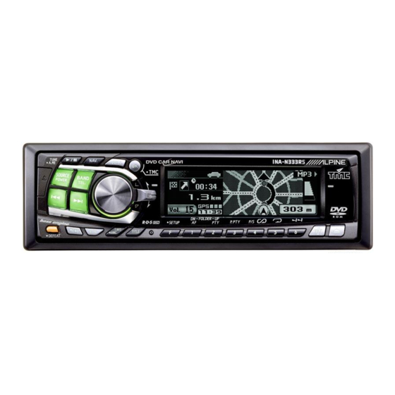
- Page 1 SERVICE MANUAL GPS Car Navigation / CD Receiver - Confidential - "Schematic Diagram (ECU P.W.Board / ASSY,FPC SHEET SW) cannot use a reference function" INA-N333RS (INA-N333RS) 3 /04-A 68E36308S01 INA-N333RS/ INA-N333RRS...
- Page 2 <Cautions for Safe Repair Work> The following cautions will prevent accidents in the workplace and will ensure safe products. *The symbols indicate caution is needed to prevent injuries and damage to property. The symbols and their meanings follow. If you ignore this symbol and handle the product incorrectly or unsafely, Warning serious injury or death may result.
- Page 3 INA-N333RS/INA-N333RRS Contents Packing Assembly Parts List Packing Method View System Connection 5 to 7 Specifications 8 , 9 I/O Interface 10 to 16 Extension Cable Adjustment Procedures 18 , 19 Block Diagram 20, 21 Parts Layout on P.W.Boards and Wiring Diagram...
-
Page 4: Packing Assembly Parts List
INA-N333RS/INA-N333RRS Packing Assembly Parts List Symbol Part No. Description Symbol Part No. Description 101-1 03S60820Y16 SCR,MCH 5X8 ZN A 101-2 03S60824Y01 SCR,WAV 1.7X4 ZN A 101-3 36A11113W01 CAP,RUBBER(A) 101-4 03A60836Y01 SCR,CUS 5X7 ZN A 01T15359Y14 ASSY,ISO CONN N033RS 01T85385W04 GPS ANT,GPA-CG2C1... -
Page 5: System Connection
INA-N333RS/INA-N333RRS System Connection <Connection> ISO Antenna Converter Plug Antenna ISO Antenna Plug (Yellow/Blue) PARKING BRAKE To the parking brake signal line (Pink/Black) AUDIO INTERRUPT IN To vehicle phone (Blue/White) REMOTE TURN-ON To amplifier or equalizer (Orange) DIMMER To the instrument cluster... - Page 6 • Connect the ground lead securely to a bare metal spot (remove any paint, dirt or gr ease if necessary) of the car chassis. • If you add an optional noise suppressor, connect it as far away from the unit as possible. Y our Alpine dealer carries various noise suppressors, contact them for further information.
- Page 7 INA-N333RS/INA-N333RRS <Connection with optional RDS-TMC Receiver Box TMC-001P> <INA-N333RS/INA-N333RRS> TMC-001P ACC (Ignition) (Red) Attached antenna Ignition Key Battery lead (Yellow) Ground (Black) Battery TMC-001P TMC Receiver Box (Sold Separately) For further information about the connection and installation of TMC-001P, refer to the owner's manual of TMC-001P.
-
Page 8: Specifications
INA-N333RS/INA-N333RRS Specifications <FM RADIO> Intermediate Frequency ......................... 10.7±0.1MHz Frequency Range ..........................87.5 to 108MHz Usable Sensitivity (Mono, 30dB S/N, at 98.1MHz) ..................20.2dBf -3dB Limiting Sensitivity (at 98.1MHz) ......................21.2dBf Residual Noise (Ref. 400Hz (narrow), at 98.1MHz) ..................28±10dB S/N Ratio (at 98.1MHz) ......................... - Page 9 INA-N333RS/INA-N333RRS <CD SECTION> System ........................Optical (Compact Disc System) Channel Balance (TCD-782, 1kHz) ........................0±3dB Distortion (TCD-782, 1kHz) ..........................0.1% Frequency Response (TCD-782, Ref. 997Hz) ..................17Hz : 0±3dB 127Hz : 0±2dB 10.007kHz : 0±2dB 19.997kHz : 0±4dB S/N Ratio (TCD-782) ............................80dB Separation (TCD-782, 1kHz) ..........................
- Page 10 INA-N333RS/INA-N333RRS TO CONTENTS - 10 -...
- Page 11 INA-N333RS/INA-N333RRS TO CONTENTS - 11 -...
- Page 12 INA-N333RS/INA-N333RRS TO CONTENTS - 12 -...
- Page 13 INA-N333RS/INA-N333RRS TO CONTENTS - 13 -...
- Page 14 INA-N333RS/INA-N333RRS TO CONTENTS - 14 -...
- Page 15 INA-N333RS/INA-N333RRS TO CONTENTS - 15 -...
- Page 16 INA-N333RS/INA-N333RRS TO CONTENTS - 16 -...
-
Page 17: Extension Cable
INA-N333RS/INA-N333RRS Extension Cable * When repairing or measuring the voltage of this unit, connect with the Extension Cable as shown in below. DVD Deck Mechanism Extension Cable (01E33127S01) Extension Cable (01E30083S01) SUB P.W.Board ASSY, NAVI CARD V-245 Extension Cable (01V33125S01) MAIN P.W.Board... -
Page 18: Adjustment Procedures
INA-N333RS/INA-N333RRS Adjustment Procedures 1. Tuner Adjustment -1. FM SECTION (1) Dummy Antenna Circuit 10ohm 45ohm Input 60ohm Output For 50 ohm FM Signal Generator Figure 1 (2) Connection DC Volt Meter Antenna Receptacle TP503 FM Dummy TP504 Antenna Unit Under Test... - Page 19 INA-N333RS/INA-N333RRS -2. AM SECTION (1) Dummy Antenna Circuit 30ohm 15pF 65pF Input Output For 50 ohm AM Signal Generator Figure 3 (2) Connection DC Volt Meter Antenna Receptacle TP503 AM Dummy TP504 Antenna Unit Under Test AM Signal Generator Figure 4...
- Page 20 Block Diagram INA-N333RS/INA-N333RRS (signal Block) JASO ANTENNA WIRE ST MULTICHIP-IC Ai-NET AUDIO PREOUT-FRONT AUDIO TUNER EEP-ROM POWER-IC PROCESSOR PREOUT-REAR BUFFER PREOUT-SUB.W 4ch SP-OUT FAN+B TEL-MUTE CIRCUIT Ai-NET Hi CIRCUIT ACC-DET CIRCUIT MAIN u-COM SYSTEM RESET/BATT-DET DVD MECHA REMO-CON (DV33M010) SERVO+5V SW...
- Page 21 INA-N333RS/INA-N333RRS (POWER SUPPLY Block) NAVI CARD 3.3V 3.3V REG 1.2A MAX. 500mA MAX. SYSTEM NAVI-ON 5V 3.3V BACK-UP 3.3V REG REGULATOR-IC 1mA MAX. BATT at usually 5V power supply 500mA MAX. BATT 5V Ope : 40mA MAX. MAIN u-COM GPS RECEIVER Erase : 100mA MAX.
- Page 22 INA-N333RS/INA-N333RRS Parts Layout on P.W.Boards and Wiring Diagram (1/5) TO CONTENTS MAIN P.W.Board (Component Side View) Orange Color Pattern:Component Side Pattern Blue Color Pattern:Foil Side Pattern - 22 -...
- Page 23 R867 Q866 C883 R837 C875 Q872 C881 Q881 Q865 R872 R833 R834 R881 R835 R836 NOTE:#1:For INA-N333RS Model Only, R873 R634 R633 $1:For INA-N333RRS Model Only, Others:Common. Orange Color Pattern:Component Side Pattern Blue Color Pattern:Foil Side Pattern - 23 -...
- Page 24 Parts Layout on P.W.Boards and Wiring Diagram (3/5) INA-N333RS/INA-N333RRS TO CONTENTS FRONT P.W.Board (Component Side View) LD911 LD913 LD910 SW903 LD914 R1116 SW904 R1045 RA909 R1083 SW905 C918 R1046 R917 C904 R1089 R919 SW907 C917 SW908 LD909 R1098 R968 R1088...
- Page 25 Parts Layout on P.W.Boards and Wiring Diagram (4/5) INA-N333RS/INA-N333RRS TO CONTENTS AMP P.W.Board IC101 (Component Side View) AMP P.W.Board (Foil Side View) SUB P.W.Board Orange Color Pattern:Component Side Pattern Blue Color Pattern:Foil Side Pattern (Component Side View) - 25 -...
- Page 26 Parts Layout on P.W.Boards and Wiring Diagram (5/5) INA-N333RS/INA-N333RRS TO CONTENTS MAIN-LSI P.W.Board MAIN-LSI P.W.Board (Foil Side View) (Component Side View) FPC,LOAD P.W.Board (Foil Side View) R121 R128 SW405 R120 R118 R129 R119 R127 CB101 R123 R208 RA101 TP406 RA104...
- Page 27 L001 2.2uH IC087 TC7S66F Q001 2SA1774 E006 E007 E013 22/16 22/16 N.U. Q002 XN1A311 C018 C019 C025 N.U. N.U. 0.01 Q005 UN9215J XL002 CFWLA450K C086 CF001 IC086 Q086 SFELA10M7 TC7S66F UN9212J R021 L021 BK1608HM102 R004 R074 100k C028 L007 C073 68uH 0.22 R068...
- Page 28 TP502 R543 CB081 R559 R508 N.U. R507 R506 R560 CB591 Z581 FH12-20S CKD510JB1H221S R581 100-1/4 Q581 UN9211J CB583 RA508 53253-0310 1kx4 TP591 R538 RA512 1kx4 TP592 R583 2.2k-1/4 TP593 TP532 R504 D501 MA113 R509 R505 TP594 L504 R503 470k BK1608HM102 TP533 TP595 TP531...
- Page 29 SW201 SLD-42-508X R292 R291 C223 C225 C226 C224 CB201 CON, TCP9389-11 R225 R221 C221 2.2u Q221 R222 C222 XN0F256 R226 2.2u R231 C231 R235 2.2u Q231 XN0F256 R232 C232 R236 2.2u ET221 R251 CB221 ASSY, WIRE RCA N033R0 R293 53253-0910 R255 C251 2.2u...
- Page 30 Q861 2SB1188 Q841 Q862 2SB1198K UN9211J CB841 53253-0210 R854 R851 R811 220kF N.U.-1/4 1.8k-1/4 M841 R855 R852 MOTOR, F3010CU-12UCV Q842 UN9212J 1.8k-1/4 1.8k-1/4 R856 R853 IC811 Q852 1.8k-1/4 1.8k-1/4 2SA1797 L5952 L854 L853 R857 Q811 C819 1000uH D864 IC864 XN1A312 BLM21PG221SH1 D851 1.8k-1/4...
- Page 31 R1115 OELD901 OELD, UEL10010 IC991 S-80935CLMC-T2 TP965 R1003 Q991 IC911 UN9212J M66710FP R1001 IC912 S-81233SGUP-T1 IC902 MBM29F800T90 Q907 2SB1198K RA907 68x4 Q908 UN9212J RA908 68x4 R913 RA909 R1080 CB904 68x4 FH12-30S-0.5S R972 IC901 M30803FGGP R966 R1081 R967 R1082 R916 R968 R1083 R969 R1084...
- Page 32 CB701 IMSA9632S-20Y L701 220uH CB703 R715 IMSA9631S-50Y R706 L704 0-1/4 BK1608HM102 R701 L705 BK1608HM102 R702 L702 R711 BLM21PG221SH1 0-1/4 BLM21PG221SH1 R713 L703 0-1/4 CB702 R716 IMSA9631S-30Y 0-1/4 R714 0-1/4 R709 100-1/4 R708 0-1/4 TP701 R703 0-1/4 TO P. W. BOARD TO PARTS LIST TO CONTENTS - 32 -...
- Page 33 C278 R278 2.2-1/4 R277 2.2-1/4 C277 CH271 R274 2.2-1/4 IMSA9110S-13 C274 R273 C273 2.2-1/4 C271 R271 2.2-1/4 C272 R272 2.2-1/4 C275 R275 2.2-1/4 C276 R276 2.2-1/4 TO P. W. BOARD TO PARTS LIST TO CONTENTS - 33 -...
- Page 34 LD11 LD12 BR1111C BR1111C SBX3050-02 SW10 1211C-27 1211C-27 1211C-27 1211C-27 1211C-27 1211C-27 1211C-27 TO P. W. BOARD TO PARTS LIST TO CONTENTS - 34 -...
- Page 35 Schematic Diagram (9/14) NOTE : 1. This is the control circuit of the Assy., ECU P .W.Board of INA-N333RS/INA-N333RRS 2. This ECU has three types of connectors CN1 -CN3 for connection of input/output to/from an external unit, and is provided on the P.W.Board.
- Page 36 INA-N333RS/INA-N333RRS Scematic Diagram (10/14) VOICE SIGNAL CONVERTER Function A/D CONVERTER Function ECU P.W.Board (2/4) "Schematic Diagram cannot use a reference function" TO P. W. BOARD TO PARTS LIST TO CONTENTS - 36 - - 36 -...
- Page 37 INA-N333RS/INA-N333RRS Schematic Diagram (11/14) CENTER PROCESSING OPERATION Function BACK-UP MEMORY Function PROGRAM MEMORY Function (correspondence MASK-ROM) SYSTEM CONTROL Function ECU P.W.Board (3/4) "Schematic Diagram cannot use a reference function" TO P. W. BOARD TO PARTS LIST TO CONTENTS - 37 -...
- Page 38 INA-N333RS/INA-N333RRS Schematic Diagram (12/14) 5V CONVERTER Function DVD PLAYER I/F Function connect of VCC, GND and not used terminal ECU P.W.Board (4/4) "Schematic Diagram cannot use a reference function" TO P. W. BOARD TO PARTS LIST TO CONTENTS - 38 -...
- Page 39 Q506 FMC2 TP307 DVLD+ TP308 C518 DVLD- C519 Q507 2SB1132 C522 TP447 RFOUT TP312 TP313 OFTR TP453 RFDIF Q508 2SB1132 R519 TP318 ARF+ R520 TP319 ARF- HD101 PICKUP, ED21A010 TP322 CB602 VHALF 54104-3292 TP321 C507 TP323 TP325 VREF2 TP320 C804 C806 C807 TP324...
- Page 40 TP210 AVDD CB401 R717 R707 52745-1690 TP212 R718 R708 UVCC TP213 UGND IC701 TP214 NJM2871F33 E702 R407 4.7k 47/10 TP216 R422 4.7k TP215 R406 4.7k TP218 UCTX TP204 TP202 TP219 VDD18 IC202 VDD3 SD603 TP220 UCRX R409 C450 N.U. NJU7223DL1 MA713 TP221 C451...
-
Page 41: Terminal Voltage Of Ic/Tr
INA-N333RS/INA-N333RRS Terminal Voltage of IC/TR IC001 IC071 PULSE(4.8) IC086 PULSE(4.8) PULSE(3.0) PULSE(4.8) IC087 PULSE(0.6) PULSE(4.0) PULSE(4.8) PULSE(3.6) PULSE(4.8) IC091 IC261 10.8 PULSE(2.6) 14.2 14.2 PULSE(3.0) 10.8 PULSE(2.6) PULSE(3.0) 10.8 TO SCHEMATIC TO CONTENTS - 41 -... - Page 42 INA-N333RS/INA-N333RRS IC281 IC501 PULSE(1.2) PULSE(2.6) PULSE(0.8) PULSE(3.4) IC282 PULSE(2.4) IC521 IC581 IC651 PULSE(4.2) IC702 IC811 PULSE(3.2) PULSE(3.2) PULSE(3.2) 14.2 14.2 14.2 TO SCHEMATIC TO CONTENTS - 42 -...
- Page 43 INA-N333RS/INA-N333RRS IC851 IC864 IC871 PULSE(17.4) PULSE(13.8) PULSE(0.6) PULSE(1.2) 13.8 PULSE(13.8) PULSE(13.8) IC881 IC891 14.2 PULSE(13.4) 11.4 11.4 IC901 PULSE(4.8) PULSE(5.2) PULSE(4.8) PULSE(5.0) PULSE(2.0) PULSE(5.0) TO CONTENTS TO SCHEMATIC - 43 -...
- Page 44 INA-N333RS/INA-N333RRS IC902 PULSE(5.0) IC909 IC910 PULSE(5.0) PULSE(5.0) PULSE(5.0) PULSE(5.0) PULSE(5.0) PULSE(5.0) PULSE(5.0) PULSE(5.0) PULSE(5.0) PULSE(5.0) PULSE(5.0) PULSE(5.0) PULSE(5.0) IC911 IC912 PULSE(4.9) PULSE(4.9) PULSE(2.0) 3.36 PULSE(4.9) IC991 PULSE(1.9) PULSE(2.5) PULSE(4.9) PULSE(1.84) PULSE(4.9) PULSE(4.9) PULSE(4.8) PULSE(4.9) PULSE(4.9) Ref. No. Q221 13.4 13.4 Q231 13.4...
- Page 45 INA-N333RS/INA-N333RRS Ref. No. Q002 Q004 Q081 Q621 Q622 Q625 13.4 13.6 Q628 4.83 Q811 Q872 13.6 13.4 13.4 13.4 Q899 13.6 13.6 Q903 Q904 Ref. No. Q003 Ref. No. Ref. No. Q001 Q841 Q005 Q842 Q062 Q846 13.6 13.6 Q086...
- Page 46 INA-N333RS/INA-N333RRS (DVD Deck Mechanism) NOTE : DATA, ADDRESS, DIGITAL, PWM : Low/High switching Digital Signal by 0V/3.3V ANALOG : usually changing Signal RF : High-frequency RF Signal IC201 IC301 CLOCK 3.29 4.83 3.28 1.63 3.27 3.15 1.64 3.27 ANALOG ADDRESS...
- Page 47 INA-N333RS/INA-N333RRS IC401 IC402 3.29 3.28 3.29 DATA 3.29 DATA 3.29 DATA 3.23 DATA 3.22 3.29 ADDRESS 1.65 ADDRESS 3.29 DATA 1.71 ADDRESS DATA ADDRESS IC403 DATA 2.99 ADDRESS DATA 3.3.6 ADDRESS 1.37 ADDRESS 1.63 ADDRESS 1.63 3.28 ADDRESS 3.29 3.23 1.64...
- Page 48 INA-N333RS/INA-N333RRS IC601 IC701 3.06 1.68 6.97 3.06 1.65 3.08 6.87 1.33 3.08 6.87 3.37 3.08 6.87 6.97 3.08 ANALOG 1.26 ANALOG Q506 ANALOG 3.05 ANALOG 6.86 ANALOG 4.69 3.05 4.81 3.27 Q507 6.87 3.56 3.05 ANALOG 2.33 6.85 ANALOG 6.85...
- Page 49 INA-N333RS/INA-N333RRS Description of IC Terminal D70F3032BGF : IC501 Symbol Terminal Description RDS-TX RDS monitor data output terminal. VPP2/HS VPP2 for Handshake Mode or HS connect terminal. TU-SDA(7511) I/O 7511-IIC data signal input/output terminal. No connect terminal. TU-SCL(7511) 7511-IIC clock signal output terminal.
- Page 50 INA-N333RS/INA-N333RRS Symbol Terminal Description F-SHIFT V3 power supply PWM control variable output terminal. DOOR-LED Door light signal output terminal. MECH-MUTE MUTE signal input terminal from DVD Mechanism. (H : MUTE) I2C-RST IIC RESET signal output terminal to VDD-IC. VHH LV-1 VHH voltage level control terminal.
- Page 51 INA-N333RS/INA-N333RRS Symbol Terminal Description N-St Audio u-COM communication start signal input terminal. IS-BUS-FIN Internal serial BUS frame signal input detection terminal. REMOCON Remote control signal input terminal. D-Rx Audio u-COM data input terminal. D-Tx Audio u-COM data output terminal. A-CLK Audio u-COM CLK output terminal.
- Page 52 INA-N333RS/INA-N333RRS Symbol Terminal Description No connect terminal. Pull-up connect terminal. (connected GND at writing) No connect terminal. RD output terminal for OELD driver IC (M66710FP). BHE output terminal for OELD driver IC (M66710FP). LWR output terminal for OELD driver IC (M66710FP).
- Page 53 INA-N333RS/INA-N333RRS Symbol Terminal Description External ROM data-BUS input terminal. OELD driver IC (M66710FP) data-BUS input/output terminal. Key matrix input signal input terminal. AVSS A/D converter GND potential terminal. DIR-L Direction indicator LEFT output terminal. VREF A/D converter ANALOG potential terminal.
- Page 54 INA-N333RS/INA-N333RRS Symbol Terminal Description OSCI High-speed OSC input terminal. OSC0 High-speed OSC output terminal. GND potential supply terminal. No connect terminal. /NMI(PULL-UP) Pull-up connect terminal. /RST HARD RESET input terminal from power supply/HOST. No connect terminal. /INT0 MN103S26E /INT0 signal terminal.
- Page 55 INA-N333RS/INA-N333RRS Symbol Terminal Description Discrimination input terminal of correspondence both 8cm Disc and CD MODE_SEL (connected pull-up)/or not (connected pull-down). I/O E2P-ROM SDA signal terminal. E2P-ROM SCL signal terminal. DCFLTCNT FEP filter switching terminal. HFMCNT High-frequency upon another control output terminal. (connected pull-down) DRVCNT1 Driver logic control output-1 terminal.
- Page 56 INA-N333RS/INA-N333RRS Exploded View (Cabinet) (1/2) 11 X2 31 X2 ET583 11 X2 CB801 ET221 CB201 ANT001 SW631 SW632 M841 6 X2 SW902 CB901 CH571 OELD901 NOTE : The place of the connection of (T) as shown in ( ), is mentioned in the "Exploded View (Cabinet) (2/2)."...
- Page 57 INA-N333RS/INA-N333RRS Exploded View (Cabinet) (2/2) CH891 M891 ..point of GREASE applied. NOTE : The place of the connection of (T) GREASE, E-PAST ( 11S42419J09 ) as shown in ( ), is mentioned in the "Exploded View (Cabinet) (1/2)." GREASE, G-8007 ( 11S41558Y01 )
- Page 58 INA-N333RS/INA-N333RRS Exploded View (DVD Deck Mechanism) (DV33M01B) TO PARTS LIST TO CONTENTS - 58 -...
-
Page 59: Electrical Parts List
INA-N333RS/INA-N333RRS Electrical Parts List Note : #1 : For INA-N333RS Model Only, $1 : For INA-N333RRS Model Only, Others : Common. * Each parts on P.W.Board are described in order of the reference number. =======MAIN P.W.Board C001 08S45676W80 CAP,CER 223K-B1E -CP... - Page 60 INA-N333RS/INA-N333RRS C055 08S45677W36 CAP,CER.101J-CH1H-CP C056 08S45676W80 CAP,CER 223K-B1E -CP C057 08S45676W73 CAP,CER.103K-B1H -CP C060 08S35374W08 CAP,CER 474K-B1C -CP C061 08S35374W08 CAP,CER 474K-B1C -CP C062 08S35349Y13 CAP,CER 684K-B1A -CP C063 08S45676W85 CAP,CER 104K-B1C -CP C064 08S45677W60 CAP,CER 102J-CH1H-CP C065 08S45676W75 CAP,CER.153K-B1H -CP...
- Page 61 INA-N333RS/INA-N333RRS C503 08S45677W12 CAP,CER.10RD-CH1H-CP C504 08S45677W12 CAP,CER.10RD-CH1H-CP C505 08S45676W73 CAP,CER.103K-B1H -CP C506 08S45676W80 CAP,CER 223K-B1E -CP C507 08S35349Y16 CAP,CER 105K-B1A -CP C508 08S45676W73 CAP,CER.103K-B1H -CP C509 08S45676W73 CAP,CER.103K-B1H -CP C510 08S45676W73 CAP,CER.103K-B1H -CP C511 08S45676W73 CAP,CER.103K-B1H -CP C512 08S45677W46 CAP,CER 271J-CH1H-CP...
- Page 62 INA-N333RS/INA-N333RRS C811 08S45676W80 CAP,CER 223K-B1E -CP C812 08S45676W80 CAP,CER 223K-B1E -CP C813 08S45676W80 CAP,CER 223K-B1E -CP C814 08S45676W80 CAP,CER 223K-B1E -CP C815 08S45676W80 CAP,CER 223K-B1E -CP C816 08S45676W80 CAP,CER 223K-B1E -CP C817 08S45676W80 CAP,CER 223K-B1E -CP C818 08T55401W37 CAP,TF 104J-1H...
- Page 63 INA-N333RS/INA-N333RRS D601 48T15706Y02 DIO,MA132WK-TX D611 48T15706Y02 DIO,MA132WK-TX D621 48T25665Y01 DIO,1SS355-TE17 -CP D651 48T15707Y01 DIO,MA133-TX D665 48T25593Y01 DIO,S1G-6904 D801 48T25593Y01 DIO,S1G-6904 D821 48T85270W02 DIO,MPG06G D826 48T85357W01 DIO,1PS226 D851 48T45286Y01 DIO,SHT RB050L-40-E1 D864 48T55105Y01 DIO,SHT RB161M-20-CP D871 48T45286Y01 DIO,SHT RB050L-40-E1 D881 48T45286Y01...
- Page 64 INA-N333RS/INA-N333RRS IC001 51T65382Y01 TDA7518 IC071 51T93333F02 NJM2904V-TE2 -SE2 IC086 51T15731W10 TC7S66F-TE85L IC087 51T15731W10 TC7S66F-TE85L IC091 51T15132Y02 SAA6588T -SE9 IC261 51T45495Y02 TA8270H(A) IC281 51T25576W07 NJM4580V-TE2 -SE2 IC282 51T25576W07 NJM4580V-TE2 -SE2 IC501 53-00675Z02 MTP,D70F3032BGF IC521 51T55070W05 MB88385CPF-ER -SE9 IC581 51T45360Y01 TC7WH14FK-TE85L -CP...
- Page 65 INA-N333RS/INA-N333RRS LD632 48T65477W05 LED,SML-010DTT87 -CP(AMB) LD632 48T65477W02 LED,SML-010LTT87 -CP(AMB) Q001 48T15657Y01 TR,2SA1774-TL Q002 48T45594W16 TR,XN1A311-TX Q003 48T16465W01 FET,CP.3SK195-Y-R Q004 48T15606Y01 FET,FC18-TL Q005 48T25137Y05 TR,UN9215J-TX Q062 48T25137Y02 TR,UN9212J-TX Q081 48T45594W12 TR ,XN1A312 -TX-CP Q086 48T25137Y02 TR,UN9212J-TX Q221 48T25317Y01 TR,XN0F256-TX Q231 48T25317Y01...
- Page 66 INA-N333RS/INA-N333RRS Q898 48T92368F04 TR,2SD1760 R Q899 48T45594W12 TR ,XN1A312 -TX-CP Q1851 48T55462Y02 TR,2SB1132-R-T100-E2 Q1852 48T25137Y02 TR,UN9212J-TX R001 06S45674W69 RES,RK 332J 1/10 -CP R002 06S45674W61 RES,RK 152J 1/10 -CP R004 06S45674W17 RES,RK 22RJ 1/10 -CP R005 06S45674W17 RES,RK 22RJ 1/10 -CP...
- Page 67 INA-N333RS/INA-N333RRS R098 06S45674W81 RES,RK 103J 1/10 -CP R099 06S45674W81 RES,RK 103J 1/10 -CP R221 06S45674W41 RES,RK 221J 1/10 -CP R222 06S45674W41 RES,RK 221J 1/10 -CP R223 06S45674W89 RES,RK 223J 1/10 -CP R224 06S45674W89 RES,RK 223J 1/10 -CP R225 06S45674W33 RES,RK 101J 1/10 -CP...
- Page 68 INA-N333RS/INA-N333RRS R514 06S45675W43 RES,RK JUMPER1/10-CP R515 06S45674W57 RES,RK 102J 1/10 -CP R516 06S45674W97 RES,RK 473J 1/10 -CP R517 06S45674W49 RES,RK 471J 1/10 -CP R518 06S45674W49 RES,RK 471J 1/10 -CP R519 06S45674W97 RES,RK 473J 1/10 -CP R520 06S45674W89 RES,RK 223J 1/10 -CP...
- Page 69 INA-N333RS/INA-N333RRS R583 06S70072F61 RES,CP .222-J-1/4-CP R584 06S45675W06 RES,RK 104J 1/10 -CP R587 06S64995F53 RES,RK 102J 1/8 -CP R588 06S64995F53 RES,RK 102J 1/8 -CP R589 06S64995F53 RES,RK 102J 1/8 -CP R590 06S45674W33 RES,RK 101J 1/10 -CP R593 06S45675W06 RES,RK 104J 1/10 -CP...
- Page 70 INA-N333RS/INA-N333RRS R818 06S15594Y06 RES,RK 224F 1/10 -CP R819 06S15593Y93 RES,RK 683F 1/10 -CP R820 06S45674W81 RES,RK 103J 1/10 -CP R821 06S70072F77 RES,CP .103-J-1/4-CP R822 06S70072F61 RES,CP .222-J-1/4-CP R823 06S45674W81 RES,RK 103J 1/10 -CP R824 06S45674W81 RES,RK 103J 1/10 -CP R825 06S70072F59 RES,CP .182-J-1/4-CP...
- Page 71 INA-N333RS/INA-N333RRS R883 06S15593Y63 RES,RK 392F 1/10 -CP R885 06S15593Y39 RES,RK 391F 1/10 -CP R886 06S15593Y49 RES,RK 102F 1/10 -CP R887 06S15593Y25 RES,RK 101F 1/10 -CP R891 06S70072F17 RES,CP .33R-J-1/4-CP R892 06S70072F17 RES,CP .33R-J-1/4-CP R893 06S70072F17 RES,CP .33R-J-1/4-CP R894 06S70072F17 RES,CP .33R-J-1/4-CP...
- Page 72 INA-N333RS/INA-N333RRS ZD891 48T15541Y44 DIO,ZEN MAZS0430H-CP ZD898 48T15542Y11 DIO,ZEN MA1Z120 -E1 =======FRONT P.W.Board C901 08S45677W12 CAP,CER.10RD-CH1H-CP C902 08S45677W10 CAP,CER 8R0D-CH1H-CP C904 08S45676W80 CAP,CER 223K-B1E -CP C905 08S45676W80 CAP,CER 223K-B1E -CP C907 08S45676W80 CAP,CER 223K-B1E -CP C909 08S45676W85 CAP,CER 104K-B1C -CP C910...
- Page 73 INA-N333RS/INA-N333RRS LD905 48T15110Y15 LED,A/G 1211C-27 -CP LD905 48T15110Y03 LED,R/G BRBG1211C-CP LD906 48T15110Y15 LED,A/G 1211C-27 -CP LD906 48T15110Y03 LED,R/G BRBG1211C-CP LD907 48T15110Y15 LED,A/G 1211C-27 -CP LD907 48T15110Y03 LED,R/G BRBG1211C-CP LD908 48T15110Y15 LED,A/G 1211C-27 -CP LD908 48T15110Y03 LED,R/G BRBG1211C-CP LD909 48T15110Y15 LED,A/G 1211C-27 -CP...
- Page 74 INA-N333RS/INA-N333RRS R915 06S64995F53 RES,RK 102J 1/8 -CP R916 06S45674W33 RES,RK 101J 1/10 -CP R917 06S45674W33 RES,RK 101J 1/10 -CP R918 06S45674W81 RES,RK 103J 1/10 -CP R919 06S45674W29 RES,RK 68RJ 1/10 -CP R925 06S45675W06 RES,RK 104J 1/10 -CP R927 06S45674W29 RES,RK 68RJ 1/10 -CP...
- Page 75 INA-N333RS/INA-N333RRS R1012 06S55361Y57 RES,RK 471J 1/4 -CP R1014 06S70072F47 RES,CP .561-J-1/4-CP R1022 06S70072F51 RES,CP .821-J-1/4-CP R1022 06S70072F61 RES,CP .222-J-1/4-CP R1024 06S70072F51 RES,CP .821-J-1/4-CP R1024 06S70072F61 RES,CP .222-J-1/4-CP R1025 06S70072F43 RES,CP .391-J-1/4-CP R1025 06S70072F53 RES,CP .102-J-1/4-CP R1026 06S70072F51 RES,CP .821-J-1/4-CP R1026 06S70072F55 RES,CP .122-J-1/4-CP...
- Page 76 INA-N333RS/INA-N333RRS R1095 06S45675W06 RES,RK 104J 1/10 -CP R1096 06S45675W06 RES,RK 104J 1/10 -CP R1097 06S45675W06 RES,RK 104J 1/10 -CP R1098 06S45675W06 RES,RK 104J 1/10 -CP R1099 06S45675W06 RES,RK 104J 1/10 -CP R1100 06S45675W06 RES,RK 104J 1/10 -CP R1101 06S45675W06 RES,RK 104J 1/10 -CP...
- Page 77 INA-N333RS/INA-N333RRS Z903 91T15058Y07 EMI,NFE31PT222Z1E-CP ZD902 48T15541Y50 DIO,ZEN MAZS0510H-CP ZD903 48T15541Y50 DIO,ZEN MAZS0510H-CP =======SUB P.W.Board C701 08T81833F13 CAP,CER 106K-B1C -CP C702 08T81833F13 CAP,CER 106K-B1C -CP C703 08T81833F13 CAP,CER 106K-B1C -CP C705 08T81833F13 CAP,CER 106K-B1C -CP C706 08T81833F13 CAP,CER 106K-B1C -CP C707...
- Page 78 INA-N333RS/INA-N333RRS R278 06S70072F78 RES,CP .2R2-J-1/4-CP =======MAIN-LSI P.W.Board C101 08S45676W85 CAP,CER 104K-B1C -CP C202 08S45676W85 CAP,CER 104K-B1C -CP C203 08S45676W85 CAP,CER 104K-B1C -CP C204 08S45676W75 CAP,CER.153K-B1H -CP C205 08S45676W85 CAP,CER 104K-B1C -CP C207 08S45676W85 CAP,CER 104K-B1C -CP C301 08S45676W85 CAP,CER 104K-B1C -CP...
- Page 79 INA-N333RS/INA-N333RRS C363 08S45676W85 CAP,CER 104K-B1C -CP C364 08S45676W85 CAP,CER 104K-B1C -CP C365 08S45676W85 CAP,CER 104K-B1C -CP C401 08S45676W85 CAP,CER 104K-B1C -CP C402 08S45676W85 CAP,CER 104K-B1C -CP C403 08S45676W85 CAP,CER 104K-B1C -CP C404 08S45676W85 CAP,CER 104K-B1C -CP C405 08S45676W85 CAP,CER 104K-B1C -CP...
- Page 80 INA-N333RS/INA-N333RRS C809 08T81833F13 CAP,CER 106K-B1C -CP C810 08T81833F13 CAP,CER 106K-B1C -CP C811 08T81833F13 CAP,CER 106K-B1C -CP C812 08T65231Y01 CAP,CER 226K-BJ1A-CP C813 08T65231Y01 CAP,CER 226K-BJ1A-CP C820 08T65231Y01 CAP,CER 226K-BJ1A-CP C821 08S35374W10 CAP,CER 225K-B1A -CP C822 08S35374W10 CAP,CER 225K-B1A -CP CB101 09T45442Y50...
- Page 81 INA-N333RS/INA-N333RRS R301 06S45674W61 RES,RK 152J 1/10 -CP R302 06S45674W81 RES,RK 103J 1/10 -CP R303 06S45674W81 RES,RK 103J 1/10 -CP R304 06S45674W81 RES,RK 103J 1/10 -CP R305 06S45675W30 RES,RK 105J 1/10 -CP R306 06S45674W61 RES,RK 152J 1/10 -CP R307 06S45674W57 RES,RK 102J 1/10 -CP...
- Page 82 INA-N333RS/INA-N333RRS R421 06S45674W97 RES,RK 473J 1/10 -CP R422 06S45674W73 RES,RK 472J 1/10 -CP R423 06S45674W97 RES,RK 473J 1/10 -CP R424 06S45674W71 RES,RK 392J 1/10 -CP R425 06S45674W97 RES,RK 473J 1/10 -CP R426 06S45674W89 RES,RK 223J 1/10 -CP R427 06S45674W97 RES,RK 473J 1/10 -CP...
- Page 83 INA-N333RS/INA-N333RRS R643 06S45674W02 RES,RK 2R7J 1/10 -CP R644 06S45674W02 RES,RK 2R7J 1/10 -CP R645 06S45674W02 RES,RK 2R7J 1/10 -CP R646 06S45674W02 RES,RK 2R7J 1/10 -CP R647 06S45674W02 RES,RK 2R7J 1/10 -CP R702 06S45675W24 RES,RK 564J 1/10 -CP R707 06S45674W49 RES,RK 471J 1/10 -CP...
- Page 84 INA-N333RS/INA-N333RRS (FAN MOTOR/12V-110mA) M891 59T65085W01 MOTOR,LOAD FF-050SK (NOSE MOTOR/7V-370mA) OELD901 01T65442Y01 OELD,UEL10010 SW631 40T15494Y02 SW,DETCT SPVG13 -E6 (NOSE OPEN DET) SW632 40T15494Y01 SW,DETCT SPVG23 -E6 (NOSE CLOSE DET) SW902 40T45305Y01 ENC,EC11E0B2LB (ROTARY ENCODER VOLUME -FLIPPER SW/MODE-SEARCH) =======DV33M01B HD101 81B51264Y01 PICKUP,ED21A010...
-
Page 85: Cabinet Assembly Parts List
INA-N333RS/INA-N333RRS Cabinet Assembly Parts List Notes : * #1 : For INA-N333RS Model Only, $1 : For INA-N333RRS Model Only, Others : Common. * The part that has not PART NUMBER will not be supplied. 01V36315S01 DF NOSE UNIT N333RS... - Page 86 INA-N333RS/INA-N333RRS 14S31545Y17 INS,CVR 100X8XT0.1 15B50101Y01 SHIELD,PWR - - - - - - - - - - - HEAT,SINK L - - - - - - - - - - - HEAT,SINK S 03S60822Y22 SCR,S-T 2.6X14 ZN A 26A31722Y01 SHIELD,PLATE 14S50096Y55 INS,CVR 10X5XT0.15...
- Page 87 INA-N333RS/INA-N333RRS DVD Deck Mechanism Assembly Parts List Note : The part that has not PART NUMBER will not be supplied. 01A51490Y01 ASSY,RIV GUIDE TOP - - - - - - - - - - - CHASSIS,TOP 41A60338Y01 SPRING,DRIVE F-L 41A60339Y01...
- Page 88 INA-N333RS/INA-N333RRS 84T65143Y01 FPC,LOAD 01A51486Y01 ASSY,RIV BKT LD-R1 01A51487Y01 ASSY,RIV BKT LD-R2 44A50825Y01 GEAR,LOAD (A) 44A50826Y01 GEAR,LOAD (B) 07B51226Y01 BKT,SHAFT LOAD 03S30688Y17 SCR,MCH M1.4X2 04B41345P11 WASH,1.2X2.5X0.25 45B51235Y01 SLIDER,ARM LIFT (R) 41A60336Y01 SPRING,CLAMP-R 41A60335Y01 SPRING,CLAMP-L 41A60337Y01 SPRING,CLAMP-RTL - - - - - - - - - - -...
Need help?
Do you have a question about the INA-N333RS and is the answer not in the manual?
Questions and answers