Advertisement
Description
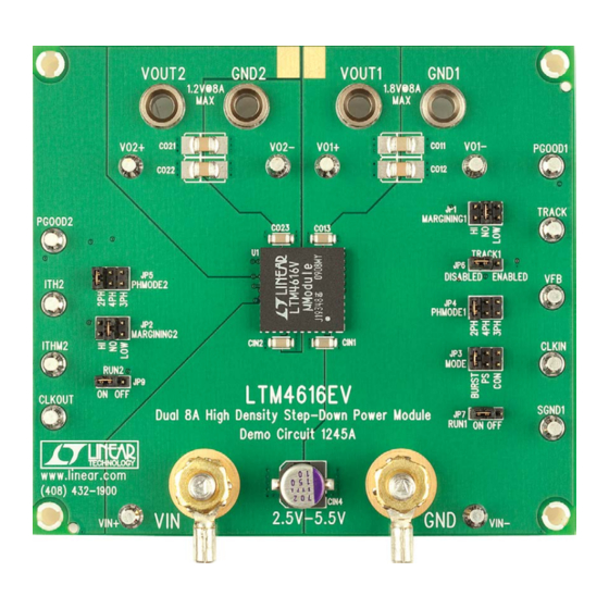
Demonstration circuit 1245A features the
high efficiency, high density, dual output switch mode
power module. The rated load current is 8A for each chan-
nel, while derating is necessary for certain V
thermal conditions. By applying a clock signal to the CLKIN
pin, the module's switching frequency may be synchronized
from 0.75MHz to 2.25MHz. The same clock frequency is
available at the CLKOUT pin with the phase relationship
between CLKIN and CLKOUT determined by the PHMODE
pin. This feature can be used not only to reduce undesirable
perForMAnce sUMMArY
PARAMETER
Input Voltage Range
Output Voltage V
OUT1
V
OUT2
Maximum Continuous Output Current
Default Operating Frequency
Efficiency
Load Transient
BoArD photo
Arrow.com.
Downloaded from
Dual 2.7V
LTM
4616, the
®
, V
, and
IN
OUT
(T
= 25°C)
A
CONDITIONS
V
= 3.3V, I
= 8A
IN
OUT1
I
= 8A
OUT2
Derating Is Necessary for Certain V
Conditions, See Data Sheet for Details
V
= 5V, V
= 1.8V, V
= 1.2V, 8A Per Channel
IN
OUT1
OUT2
V
= 3.3V, V
=1.8V; V
= 1.2V
IN
OUT1
OUT2
DEMO MANUAL DC1245A
, 8A Step-Down
IN(MIN)
µModule Regulator
frequency harmonics but also to parallel the two channels
of LTM4616 or even multiple LTM4616s and LTM4608s to
provide higher output currents. The LTM4616 data sheet
must be read in conjunction with this demo manual prior
to working on or modifying demo circuit DC1245A.
Design files for this circuit board are available at
http://www.linear.com/demo/DC1245A
L, LT, LTC, LTM, µModule, Linear Technology and the Linear logo are registered trademarks of
Linear Technology Corporation. All other trademarks are the property of their respective owners.
VALUE
2.7V to 5.5V
1.8 ±2%
1.2 ±2%
, V
, and Thermal
8A
IN
OUT
DC
1.5MHz
77.5%, See Figure 3 for More Information
See Figures 4 and 5 for Details
LTM4616
Each Channel
dc1245afa
1
Advertisement
Table of Contents

Related Manuals for Linear Technology LTM4616


Summary of Contents for Linear Technology LTM4616
- Page 1 CLKOUT pin with the phase relationship L, LT, LTC, LTM, µModule, Linear Technology and the Linear logo are registered trademarks of between CLKIN and CLKOUT determined by the PHMODE Linear Technology Corporation. All other trademarks are the property of their respective owners.
- Page 2 Demonstration circuit 1245A is an easy way to evaluate 4. Once the proper output voltage is established, adjust the performance of the LTM4616. Please refer to Figure 1 the load within the operating range and observe the for proper measurement equipment setup and follow the...
- Page 3 DEMO MANUAL DC1245A qUick stArt proceDUre 7. Channel 2 is set up to synchronize to the CLKOUT sig- nal of channel 1. The default phase difference is 180°. Please refer to data sheet for how to set up PHMODE1 and PHMODE2 for paralleling more than 2 channels. dc1245a F05 = 3.3V =1.2V...
- Page 4 Resistor, Chip, 4.99k, 1/16W, 1%, 0402 Vishay, CRCW04024K99FKED RSET2 Resistor, Chip, 10k, 1/16W, 1%, 0402 Vishay, CRCW040210K0FKED IC LTM4616EV 144-Pin LGA Linear Technology, LTM4616EV Additional Demo Board Circuit Components CO14, CO15, CO24, CO25 (OPT) Capacitor, 1210-3743 R7, R5 Resistor, Chip, 100k, 1/16W, 5%, 0402...
- Page 5 Information furnished by Linear Technology Corporation is believed to be accurate and reliable. However, no responsibility is assumed for its use. Linear Technology Corporation makes no representa- tion that the interconnection of its circuits as described herein will not infringe on existing patent rights.
- Page 6 Linear Technology Corporation (LTC) provides the enclosed product(s) under the following AS IS conditions: This demonstration board (DEMO BOARD) kit being sold or provided by Linear Technology is intended for use for ENGINEERING DEVELOPMENT OR EVALUATION PURPOSES ONLY and is not provided by LTC for commercial use. As such, the DEMO BOARD herein may not be complete in terms of required design-, marketing-, and/or manufacturing-related protective considerations, including but not limited to product safety measures typically found in finished commercial goods.
Need help?
Do you have a question about the LTM4616 and is the answer not in the manual?
Questions and answers