Table of Contents
Advertisement
Specification
n Amplifier Section
RMS OUTPUT POWER both channel
driven simultaneously
10 % Total harmonic distortion
Input impedance
MUSIC PORT
Output impedance
HEADPHONE
Phone jack
Terminal
Music Port input jack
Terminal
n FM Tuner Section
Frequency range
Sensitivity
S/N 26 dB
Antenna terminals
Preset station
n AM Tuner Section
Frequency range
Sensitivity
S/N 20 dB (at 999 kHz)
15 W per channel (6 Ω)
12 KΩ
16 to 32 Ω
Stereo, 3.5 mm
Stereo, 3.5 mm
87.5 to 108.00 MHz (50 kHz step)
0.10 µV (IHF)
1.20 µV
75 Ω (unbalanced)
FM 20 stations
AM 15 stations
522 to 1629 kHz (9 kHz steps)
520 to 1630 kHz (10 kHz steps)
1000 µV/m
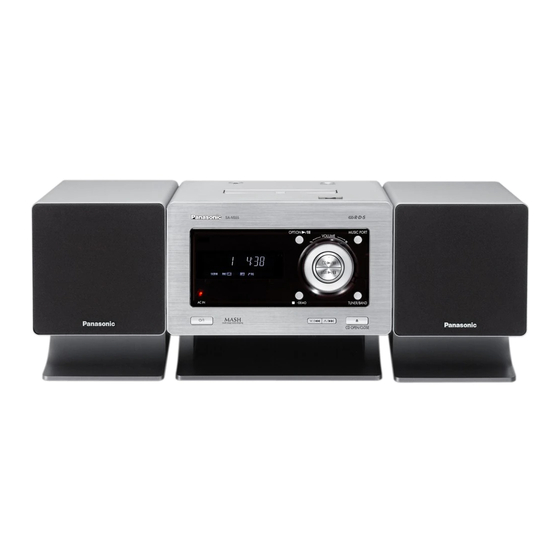
SA-NS55E
SA-NS55EG
Colour
(S)... Silver Type
n CD Section
Disc played [8 cm or 12 cm]
(1) CD-Audio (CD-DA)
(2) CD-R/RW (CD-DA, MP3 formatted disc)
(3) MP3
Sampling frequency
CD
MP3
Bit rate
MP3
Decoding
Pickup
Wavelength
Beam source
Laser power
Audio output (Disc)
Number of channels
Frequency response
Wow and flutter
Digital filter
D/A converter
n USB Section
Playable USB Storage Media
(1) HDD
(2) USB MP3 player/Digital audio player
(3) USB Thumbdrives
© 2007 Matsushita Electric Industrial Co. Ltd.. All
rights
reserved.
distribution is a violation of law.
ORDER NO. MD0703016CE
CD Stereo System
32 kHz, 44.1 kHz, 48 kHz
32 kbps to 384 kbps
16/20/24 bit linear
Semiconductor laser
20 Hz to 20 kHz (+1, -2dB)
Below measurable limit
MASH (1 bit DAC)
Unauthorized
copying
44.1 kHz
785 nm
CLASS 1
2 channel
8 fs
and
Advertisement
Table of Contents

Related Manuals for Panasonic SA-NS55E


Summary of Contents for Panasonic SA-NS55E
- Page 1 ORDER NO. MD0703016CE CD Stereo System SA-NS55E SA-NS55EG Colour (S)... Silver Type Specification n Amplifier Section n CD Section RMS OUTPUT POWER both channel Disc played [8 cm or 12 cm] driven simultaneously (1) CD-Audio (CD-DA) 10 % Total harmonic distortion (2) CD-R/RW (CD-DA, MP3 formatted disc) 15 W per channel (6 Ω)
-
Page 2: Table Of Contents
SA-NS55E / SA-NS55EG Supported audio file format Mass 3.5 kg MP3 Bit rate Operating temperature range +5 to +35°C USB memory port Operation humidity range 5 to 90% RH (no condensation) Maximum current 500mA Power consumption in standby 0.7 W (approx.) - Page 3 SA-NS55E / SA-NS55EG 15.1. CD SERVO CIRCUIT 16.4. POWER P.C.B, SWITCH P.C.B, TRANSFORMER P.C.B 15.2. MAIN CIRCUIT and AC INLET P.C.B 15.3. PANEL CIRCUIT 17 Illustration of IC's, Transistors and Diodes 15.4. TUNER EXTENT CIRCUIT, HP / MUSIC PORT CIRCUIT 18 Terminal Function of IC's 18.1.
-
Page 4: Safety Precautions
SA-NS55E / SA-NS55EG 1 Safety Precautions 1.1. General Guidelines 1. When servicing, observe the original lead dress. If a short circuit is found, replace all parts which have been overheated or damaged by the short circuit. 2. After servicing, ensure that all the protective devices such as insulation barriers, insulation papers shields are properly installed. -
Page 5: Before Repair And Adjustment
SA-NS55E / SA-NS55EG 1.2. Before Repair and Adjustment Disconnect AC power, discharge Power Supply Capacitors C321, C322, C323, C324, C325, C507, C520 and C611 through a 10Ω, 1W resistor to ground. DO NOT SHORT-CIRCUIT DIRECTLY (with a screwdriver blade, for instance), as this may destroy solid state devices. -
Page 6: Prevention Of Electro Static Discharge (Esd) To Electrostatically Sensitive (Es) Devices
SA-NS55E / SA-NS55EG 2 Prevention of Electro Static Discharge (ESD) to Electrostatically Sensitive (ES) Devices Some semiconductor (solid state) devices can be damaged easily by electricity. Such components commonly are called Electrostatically Sensitive (ES) Devices. Examples of typical ES devices are integrated circuits and some field-effect transistors and semiconductor “chip”... -
Page 7: Precaution Of Laser Diode
SA-NS55E / SA-NS55EG 3 Precaution of Laser Diode Caution : This product utilizes a laser diode with the unit turned "ON", invisible laser radiation is emitted from the pick up lens. Wavelength : 780 nm Maximum output radiation power from pick up : 100 µW/VDE Laser radiation from pick up unit is safety level, but be sure the followings: 1. -
Page 8: Handling Precautions For Traverse Deck
SA-NS55E / SA-NS55EG 4 Handling Precautions For Traverse Deck The laser diode in the traverse deck (optical pickup) may break down due to potential difference caused by static electricity of clothes or human body. So, be careful of electrostatic breakdown during repair of the traverse deck (optical pickup). -
Page 9: Handling The Lead Free Solder
SA-NS55E / SA-NS55EG 5 Handling the Lead free Solder 5.1. General description about Lead Free Solder (PbF) The lead free solder has been used in the mounting process of all electrical components on the printed circuit boards used for this equipment in considering the globally environmental conservation. -
Page 10: Accessories
SA-NS55E / SA-NS55EG 6 Accessories Note : Refer to Packing Materials & Accessories (Section 20) for part number. Remote control AC cord AM loop antenna FM antenna... -
Page 11: Operation Procedures
SA-NS55E / SA-NS55EG 7 Operation Procedures 7.1. Main Unit Key Buttons Operation 7.2. Remote Control Key Buttons Operation... -
Page 12: Disc Information
SA-NS55E / SA-NS55EG 7.3. Disc Information... -
Page 13: Self Diagnosis And Special Mode Setting
SA-NS55E / SA-NS55EG 8 Self diagnosis and special mode setting This unit is equipped with features of self-diagnostic & special mode setting for checking the functions & reliability. 8.1. Service Mode Summary Table The service modes can be activated by pressing various button combination on the main unit and remote control unit.Below is the... - Page 14 SA-NS55E / SA-NS55EG Item FL Display Key Operation Mode Name Description Front Key Doctor Mode To enter into Doctor (Display 1) In any mode: Mode for checking of 1. Press [ ] button on main unit follow various items and by [4] and [7] on remote control.
- Page 15 SA-NS55E / SA-NS55EG Item FL Display Key Operation Mode Name Description Front Key Volume Setting Check for the volume Display 1 In doctor mode: setting of the main unit. 1. Press [7] button on remote control. The volume will be...
-
Page 16: Error Code Table
SA-NS55E / SA-NS55EG Below is the procedures for this mode. Step 1: Enter into Doctor mode. (For more information, refer to section 8.2 on key operation to enter into this mode). Step 2: Press [ ], [1], [4] button on remote control. It enter into CD Self-Adjustment Test mode. (During this mode the result shall correspond to the condition as shown in the table below). -
Page 17: Assembling And Disassembling
SA-NS55E / SA-NS55EG 9 Assembling and Disassembling 9.1. Caution “ATTENTION SERVICER” Some chassis components may be have sharp edges. Be careful when disassembling and servicing. 1. This section describes procedures for checking the operation of the major printed circuit boards and replacing the main components. -
Page 18: Disassembly Flow Chart
SA-NS55E / SA-NS55EG 9.2. Disassembly flow chart The following chart is the procedure for disassembling the casing and inside parts for internal inspection when carrying out the servicing. To assemble the unit, reverse the steps shown in the chart below. -
Page 19: Main Parts Location Diagram
SA-NS55E / SA-NS55EG 9.3. Main Parts Location Diagram... -
Page 20: Disassembly Of Top Cabinet Unit
SA-NS55E / SA-NS55EG 9.4. Disassembly of Top Cabinet Unit Step 4: Detach cable (CN802, CN803A and CN806B) on Main P.C.B.. Step 5: Remove Top Cabinet as arrow shown. Step 1: Remove 4 screws. Step 2: Press gently down and push outward as per... -
Page 21: Disassembly Of D-Port And Hp / Music Port
SA-NS55E / SA-NS55EG 9.5. Disassembly of D-Port and HP 9.6. Disassembly of USB P.C.B. / Music Port P.C.B. · Follow the (Step 1) - (Step 5) of Item 9.4. · Follow the (Step 1) - (Step 5) of Item 9.4. -
Page 22: Disassembly Of Tuner Pack
SA-NS55E / SA-NS55EG 9.7. Disassembly of Tuner Pack · Follow the (Step 1) - (Step 5) of Item 9.4. Step 3: Unsolder the solder point to remove USB P.C.B.. Step 1: Remove 1 screw. Step 2: Detach cable (CN810) on Main P.C.B. to... -
Page 23: Disassembly Of Rear Cabinet Unit
SA-NS55E / SA-NS55EG 9.8. Disassembly of Rear Cabinet 9.9. Disassembly of Power and AC Unit Inlet P.C.B. · Follow the (Step 1) - (Step 5) of Item 9.4. · Follow the (Step 1) - (Step 5) of Item 9.4. · Follow the (Step 2) of Item 9.7. -
Page 24: Disassembly Of Transformer
SA-NS55E / SA-NS55EG 9.10. Disassembly of Transformer P.C.B. · Follow the (Step 1) - (Step 5) of Item 9.4. · Follow the (Step 2) of Item 9.7. · Follow the (Step 1) - (Step 4) of Item 9.8. Step 5 : Unsolder the terminal to replace the component. -
Page 25: Disassembly Of Front Panel
SA-NS55E / SA-NS55EG 9.11. Disassembly of Front Panel 9.12. Disassembly of Panel P.C.B. · Follow the (Step 1) - (Step 5) of Item 9.4. · Follow the (Step 1) - (Step 5) of Item 9.4. · Follow the (Step 1) - (Step 3) of Item 9.11. -
Page 26: Disassembly Of Main P.c.b
SA-NS55E / SA-NS55EG 9.13. Disassembly of Main P.C.B. 9.14. Disassembly of Switch P.C.B. · Follow the (Step 1) - (Step 5) of Item 9.4. · Follow the (Step 1) - (Step 5) of Item 9.4. Step 1 : Detach cable (CN700) on Motor P.C.B.. -
Page 27: Disassembly Of Motor P.c.b
SA-NS55E / SA-NS55EG 9.15. Disassembly of Motor P.C.B. · Follow the (Step 1) - (Step 5) of Item 9.4. Step 4 : Unsolder both solder point to remove the Step 1 : Detach cable (CN701B) on Main P.C.B.. motor P.C.B.. -
Page 28: Disassembly Of Gear Box
SA-NS55E / SA-NS55EG 9.16. Disassembly of Gear Box 9.17. Disassembly of CD Loading Block · Follow the (Step 1) - (Step 5) of Item 9.4. · Follow the (Step 1) - (Step 3) of Item 9.15. · Follow the (Step 1) - (Step 5) of Item 9.4. - Page 29 SA-NS55E / SA-NS55EG Step 3 : Remove 4 screws. Step 6 : Lift up & remove CD Loading block as arrow shown. Step 4 : Remove 4 screws. Step 5 : Detach connector CN805.
-
Page 30: Disassembly Of Cd Mechanism
SA-NS55E / SA-NS55EG 9.18. Disassembly of CD Mechanism · Follow the (Step 1) - (Step 5) of Item 9.4. · Follow the (Step 2) of Item 9.7. · Follow the (Step 1) - (Step 4) of Item 9.8. · Follow the (Step 1) - (Step 2) and (Step 4) of Item 9.10. - Page 31 SA-NS55E / SA-NS55EG Step 7 : Remove the Inner chassis as arrow shown. · Disassembly of CD Mechanism Note : After CD mechanism is installed, ensure the FFC cable and connecting cable wire is arrange properly as diagram shown. Step 8 : Remove 4 screws and remove CD Mechanism as arrow shown.
-
Page 32: Disassembly Of Traverse Unit, Driving Gear, And Cam Gear (Cd Mechanism Unit)
SA-NS55E / SA-NS55EG 9.19. Disassembly of Traverse Unit, Driving Gear, and Cam Gear (CD Mechanism Unit) 9.19.1. Disassembly of the Traverse Unit · Follow the (Step 1) - (Step 5) of Item 9.4. · Follow the (Step 2) of Item 9.7. - Page 33 SA-NS55E / SA-NS55EG...
- Page 34 SA-NS55E / SA-NS55EG 9.19.2. Disassembly of CD Servo P.C.B · Follow the (Step 1) - (Step 5) of Item 9.4. · Follow the (Step 2) of Item 9.7. · Follow the (Step 1) - (Step 4) of Item 9.8.
- Page 35 SA-NS55E / SA-NS55EG · Follow the (Step 1) - (Step 2) and (Step 4) of Item 9.10. · Follow the (Step 1) - (Step 3) of Item 9.11. · Follow the (Step 1) - (Step 6) of Item 9.17. · Follow the (Step 1) - (Step 8) of Item 9.18.
-
Page 36: Service Positions
SA-NS55E / SA-NS55EG 10 Service Positions Note: For description of the disassembly procedures, see the Section 9 10.1. Checking and Repairing of HP / Music Port, D-Port and USB (side B) P.C.B. -
Page 37: Checking And Repairing Of Panel P.c.b
SA-NS55E / SA-NS55EG 10.2. Checking and Repairing of Panel P.C.B. -
Page 38: Checking And Repairing Of Switch And Motor P.c.b
SA-NS55E / SA-NS55EG 10.3. Checking and Repairing of Switch and Motor P.C.B. -
Page 39: Checking And Repairing Transformer P.c.b
SA-NS55E / SA-NS55EG 10.4. Checking and Repairing Transformer P.C.B. -
Page 40: Checking And Repairing Power And Ac Inlet P.c.b
SA-NS55E / SA-NS55EG 10.5. Checking and Repairing Power and AC Inlet P.C.B. -
Page 41: Checking And Repairing Main P.c.b
SA-NS55E / SA-NS55EG 10.6. Checking and Repairing Main P.C.B. -
Page 42: Checking And Repairing Cd Servo P.c.b
SA-NS55E / SA-NS55EG 10.7. Checking and Repairing CD Servo P.C.B. -
Page 43: Voltage Measurement & Waveform Chart
SA-NS55E / SA-NS55EG 11 Voltage Measurement & Waveform Chart Note: · Indicated voltage values are the standard values for the unit measured by the DC electronic circuit tester (high-impedance) with the chassis taken as standard. Therefore, there may exist some errors in the voltage values, depending on the internal impedance of the DC circuit tester. - Page 44 SA-NS55E / SA-NS55EG 11.1.2. MAIN P.C.B.
- Page 45 SA-NS55E / SA-NS55EG 11.1.3. PANEL P.C.B...
- Page 46 SA-NS55E / SA-NS55EG 11.1.4. POWER P.C.B 11.1.5. TRANSFORMER P.C.B 11.1.6. MOTOR P.C.B...
- Page 47 SA-NS55E / SA-NS55EG 11.1.7. USB P.C.B...
-
Page 48: Waveform Chart
SA-NS55E / SA-NS55EG 11.2. Waveform Chart CN807 PIN 15 CN807 PIN 17 CN807 PIN 18 CN807 PIN 19 CD PLAY CD PLAY CD PLAY CD PLAY 3.36Vp-p (10msec.div) 3.00Vp-p (10msec.div) 2.68Vp-p (50msec.div) 2.72Vp-p (50msec.div) CN901B PIN 1 CN901B PIN 2... -
Page 49: Wiring Connection Diagram
SA-NS55E / SA-NS55EG 12 Wiring Connection Diagram 4..1 14..2 FAN UNIT JW503 13..1 CN702 PANEL P.C.B 1..13 CN901A 2. - Page 50 SA-NS55E / SA-NS55EG...
-
Page 51: Block Diagram
SA-NS55E / SA-NS55EG 13 Block Diagram 13.1. CD SERVO/ OPTICAL PICKUP UNIT... -
Page 52: Main(1/2)/ Tuner Extent/ Panel/ D Port/ Motor/ Switch
SA-NS55E / SA-NS55EG 13.2. MAIN(1/2)/ TUNER EXTENT/ PANEL/ D PORT/ MOTOR/ SWITCH... -
Page 53: Main(2/2)/ Usb Module/ Hp/Music Port/ Power/Transformer/ Ac Inlet
SA-NS55E / SA-NS55EG 13.3. MAIN(2/2)/ USB MODULE/ HP/MUSIC PORT/ POWER/TRANSFORMER/ AC INLET... - Page 54 SA-NS55E / SA-NS55EG...
-
Page 55: Notes Of Schematic Diagram
SA-NS55E / SA-NS55EG 14 Notes Of Schematic Diagram (All schematic diagrams may be modified at any time with the development of new technology) Notes: S700: Mecha-up switch. S701: Mecha-down switch. S900: Stop switch. ( S901: CD Play switch. ( S902: USB switch. - Page 56 SA-NS55E / SA-NS55EG...
-
Page 57: Schematic Diagram
15 14 12 11 R7220 R7330 W7002 W7004 5.6K C7335 X7201 C7315 IC7002 0.47 H2B169500005 BA5948FPE2 C7334 4 CH DRIVE IC C7338 10V220 0.056 R7323 R7331 3.3k R7325 R7315 3.3k R7332 R7335 TRAVERSE MOTOR SPINDLE MOTOR SA-NS55E/EG CD SERVO CIRCUIT... -
Page 58: Main Circuit
SA-NS55E / SA-NS55EG 15.2. MAIN CIRCUIT SCHEMATIC DIAGRAM - 2 : FM/AM SIGNAL LINE : IPOD SIGNAL LINE MAIN CIRCUIT : + B SIGNAL LINE : MAIN SIGNAL LINE : AUX SIGNAL LINE : CD SIGNAL LINE Q721 Q723 MPORT_L... - Page 59 SA-NS55E / SA-NS55EG SCHEMATIC DIAGRAM - 3 MAIN CIRCUIT : + B SIGNAL LINE : MAIN SIGNAL LINE : AUX SIGNAL LINE K L M N O P Q R S T U V W TO MAIN SECTION (1/3) 70 69...
- Page 60 SA-NS55E / SA-NS55EG SCHEMATIC DIAGRAM - 4 : CD SIGNAL LINE MAIN CIRCUIT : + B SIGNAL LINE : MAIN SIGNAL LINE : IPOD SIGNAL LINE TO MAIN SECTION (2/3) D602 B0ACCK000005 D601 B0ACCK000005 IC605 IC601 C0DAZYY00018 C0DBZGC00067 USB 5.0V REGULATOR IC CN807 FL3.3V REGULATOR IC...
-
Page 61: Panel Circuit
SA-NS55E / SA-NS55EG 15.3. PANEL CIRCUIT SCHEMATIC DIAGRAM - 5 PANEL CIRCUIT : + B SIGNAL LINE : - B SIGNAL LINE FL900 A2BB00000166 R319 R318 FL DISPLAY 6.8K D300 B0BC6R700006 C900 50V22 C323 50V22 VP_GND C325 50V22 VPGND KEY1... -
Page 62: Tuner Extent Circuit, Hp / Music Port Circuit And D-Port Circuit
MAIN CIRCUIT WA3004 (CN806B) IN DOCK5V DOCK_R IN SCHEMATIC WA3001 DOCK5V DOCK_DET1 DIAGRAM - 4 DOCK_DET2 (MIC_VCC) (RF_MUTE) DOCK_UOUT BATT2 AD_CTRL DO_UART_IN IPOD_DET (A/D CONT) (RF_SEL) UART_IN IPOD_DET DOCK5V WA3003 VBUS SA-NS55E/EG TUNER EXTENT / HP/MUSIC PORT / D-PORT CIRCUIT... -
Page 63: Usb Circuit
SA-NS55E / SA-NS55EG 15.5. USB CIRCUIT SCHEMATIC DIAGRAM - 7 USB CIRCUIT : + B SIGNAL LINE : USB SIGNAL LINE IC951 C0DBZYE00002 VOLTAGE REGULATOR R972 C931 16V10 R971 D3.3V R951 C914 R950 CTRL FLAG C951 DGND R957 2.2K R902... -
Page 64: Power Circuit
SA-NS55E / SA-NS55EG 15.6. POWER CIRCUIT SCHEMATIC DIAGRAM - 8 POWER CIRCUIT : + B SIGNAL LINE : MAIN SIGNAL LINE IC400 AN17831A POWER AMPLIFIER IC L270, L271, L470, L471 G0AR76Y00003 JK600 L270 C455 C255 R250 100P 100P L271 8.2K... -
Page 65: Motor Circuit And Switch Circuit
W703 R716 10V220 4.7K R710 R711 Q703 18 1/2W Q702 R713 B1ABCF000079 R731 C703 R719 D700 D702 820K 50V2.2 DC DETECT W712 CN702 D700, D702 B0ACCK000005 FAN1(+) FAN2(-) Q701 Q702 B1ACKD000006 B1ABCF000079 FAN DRIVE SWITCH SA-NS55E/EG MOTOR / SWITCH CIRCUIT... -
Page 66: Transformer Circuit And Ac Inlet Circuit
R505 R504 SWITCH R506 3.3K Q501 2SB0621AHA R501 D507 C502 W1(BROWN) VP REGULATOR 63V100 B0EAKM000117 W2(BLUE) C504 R502 0.01u 4.7K C503 63 V100 D506 B0EAKM000117 C505 R503 D508 T502 100V10 B0BC02900004 G4CYAYY00137 SUB TRANSFORMER SA-NS55E/EG TRANSFORMER / AC INLET CIRCUIT... -
Page 67: Printed Circuit Board
SA-NS55E / SA-NS55EG 16 Printed Circuit Board 16.1. CD SERVO P.C.B and USB P.C.B CD SERVO P.C.B (REPV0111A) USB P.C.B (REPV0101A) TP51 (RF) C7227 TP19 W7014 TP14 C7204 W7015 C7226 R7212 TP18 TP50 C7228 TP17 R7218 C7216 C7230 TP13 R7221... -
Page 68: Tuner Extent P.c.b, Main P.c.b, Hp/Music Port P.c.b And Motor P.c.b
SA-NS55E / SA-NS55EG 16.2. TUNER EXTENT P.C.B, MAIN P.C.B, HP/MUSIC PORT P.C.B and MOTOR P.C.B MAIN P.C.B (REPV0117A) TUNER EXTENT P.C.B (REPV0117A) CN901B Q421 Q422 W1135 JW810 9 11 13 L850 Z800 10 12 14 (ENG06823QF TUNER PACK) L851 R436... -
Page 69: Panel P.c.b And D-Port P.c.b
SA-NS55E / SA-NS55EG 16.3. PANEL P.C.B and D-PORT P.C.B PANEL P.C.B (REPV0117A) JW503 Z901 CN901A W312 SENSOR S910 S911 (MUSIC PORT) (OPTION/D-PORT) S901 (CD PLAY) FL300 R312 R311 R303 C302 C301 W302 IC300 VOLUME W304 W311 C308 VR900 C307 R304... -
Page 70: Power P.c.b, Switch P.c.b, Transformer P.c.b And Ac Inlet P.c.b
SA-NS55E / SA-NS55EG 16.4. POWER P.C.B, SWITCH P.C.B, TRANSFORMER P.C.B and AC INLET P.C.B POWER P.C.B (REPV0117A) TRANSFORMER P.C.B (REPV0117A) ZJ400 JW805 R584 W406 C505 Q600 FP600 Q501 CN503 R583 (5A) C512 IC600 R505 JW803 C504 W506 W512 R502 W507... -
Page 71: Illustration Of Ic's, Transistors And Diodes
SA-NS55E / SA-NS55EG 17 Illustration of IC's, Transistors and Diodes BA5948FPE2 (28P) C0ABBB000297 (8P) C1BB00000732 (32P) MN6627954MA(100P) C0DBZGC00067 C0CBABG00027 C0DBZYE00002 (8P) MN101EF16ZXW(100P) C1AB00002751 (16P) C0HBB0000057(44P) MNZSFB5KJM1 (64P) C0DAZYY00018 AN17831A C0DAZYY00005 C0GAG0000007 C0JBAB000884 B1ACKD000006 C0DAZYY00019 C0DAZYY00006 B0EAKM000117 2SB0621AHA B1ABGC000005 B1ADCF000001 B0ADCJ000020... -
Page 72: Terminal Function Of Ic's
SA-NS55E / SA-NS55EG 18 Terminal Function of IC's 18.1. IC7001 (MN6627954MA) IC SERVO PROCESSOR/DIGITAL SIGNAL PROCESSOR/DIGITAL FILTER D/A CONVERTER Pin No. Mark Function Pin No. Mark Function DRAM address signal O/P 11 OUTL\ Audio O/P (LCH) DRAM address signal O/P 9... -
Page 73: Ic7002 (Ba5948Fpe2) Ic 4Ch Drive
SA-NS55E / SA-NS55EG 18.2. IC7002 (BA5948FPE2) IC 4CH Drive Pin No. Mark Function Pin No. Mark Function Motor Driver Input Motor Drive (3) reverse - action output Turntable Motor Drive Signal (“L”:ON) Motor Drive (3) forward - action output Motor Drive (1) Input... - Page 74 SA-NS55E / SA-NS55EG Pin No. Mark Function MECH_RIN Mecha Movement - Reverse MECH_SFU Mecha Switch - Up MECH_SFD Mecha Switch - Down MUTE_A Analog MUTE Output(L:MUTE HP_SW Headphone SW Detect Input DlinkDET3 Dport Detect Connecting Unit CD_OPEN_ CD Open SW (H:Open;...
-
Page 75: Exploded Views
SA-NS55E / SA-NS55EG 19 Exploded Views 19.1. Cabinet Parts Location & Traverse Part Location... - Page 76 SA-NS55E / SA-NS55EG...
-
Page 77: Packaging
SA-NS55E / SA-NS55EG 19.2. Packaging... - Page 78 SA-NS55E / SA-NS55EG...
-
Page 79: Replacement Parts List
SA-NS55E / SA-NS55EG 20 Replacement Parts List Notes: · Important safety notice: Components identified by mark have special characteristics important for safety. Furthermore, special parts which have purposes of fire-retardent (resistors), high-quality sound (capacitors), low noise (resistors), etc are used. - Page 80 SA-NS55E / SA-NS55EG Ref. Part No. Part Name & Description Remarks Ref. Part No. Part Name & Description Remarks RFKNANS55P-K CLAMPER HOLDER ASS’Y QR816 B1GBCFGN0016 TRANSISTOR RME0288-1 CENTERING SPRING QR901 B1GBCFJJ0051 TRANSISTOR RMG0510-K FLOATING RUBBER (A) RMG0511-K FLOATING RUBBER (B)
- Page 81 SA-NS55E / SA-NS55EG Ref. Part No. Part Name & Description Remarks Ref. Part No. Part Name & Description Remarks CN801 K1MN06A00013 6P FFC CONNECTOR OSCILLATORS CN802 K1MN22AA0004 22P FFC CONNECTOR CN803 K1KA12AA0319 12P CONNECTOR X320 H0H433400002 CRYSTAL OSCILLATOR CN803A K1KA09AA0193...
- Page 82 SA-NS55E / SA-NS55EG Ref. Part No. Part Name & Description Remarks Ref. Part No. Part Name & Description Remarks W1138 ERJ3GEY0R00V CHIP JUMPER R204 ERJ3GEYJ682V 6.8K 1/16W W1140 ERJ3GEY0R00V CHIP JUMPER R205 D0GB472JA007 4.7K 1/16W W1142 ERJ6GEY0R00V CHIP JUMPER R207 D0GB472JA007 4.7K 1/16W...
- Page 83 SA-NS55E / SA-NS55EG Ref. Part No. Part Name & Description Remarks Ref. Part No. Part Name & Description Remarks R453 D0GB392JA007 3.9K 1/16W R816 D0GB222JA007 2.2K 1/16W R454 D0GB821JA007 820 1/16W R817 ERJ3GEYJ102V 1K 1/16W R455 D0GB563JA007 56K 1/16W R818...
- Page 84 SA-NS55E / SA-NS55EG Ref. Part No. Part Name & Description Remarks Ref. Part No. Part Name & Description Remarks R903 ERJ2GE0R00X 0 1/32W C215 ECJ1VB1H104K 0.1 50V R904 ERJ2GE0R00X 0 1/32W C230 ECA1HAK010XB 1 50V R906 ERJ2GE0R00X 0 1/32W C231...
- Page 85 SA-NS55E / SA-NS55EG Ref. Part No. Part Name & Description Remarks Ref. Part No. Part Name & Description Remarks C454 ECA1HAKR22XB 0.22 50V C811 F1H1H101A230 100P 50V C455 F1H1H101A230 100P 50V C812 F1H1H102A219 1000P 50V C457 ECQV1H224JL3 0.22 50V C813...
- Page 86 SA-NS55E / SA-NS55EG Ref. Part No. Part Name & Description Remarks C7244 ECJ1VB1C153K 0.015 16V C7253 F1H1H471A219 470P 50V C7263 ECJ1VB1C104K 0.1 16V C7264 ECJ1VB1C104K 0.1 16V C7315 F1H1A474A025 0.47 10V C7334 ECEA1AKA221I 220 10V C7335 F1H1C104A008 0.1 16V C7338 ECJ1VB1C563K 0.056 16V...
Need help?
Do you have a question about the SA-NS55E and is the answer not in the manual?
Questions and answers