Advertisement
Quick Links
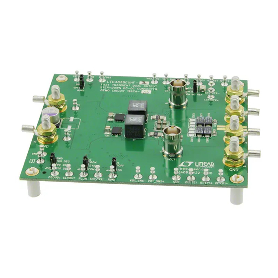
DESCRIPTION
Demonstration circuits
dual output synchronous buck converters featuring the
LTC
3838EUHF-1/LTC3838EUHF-2. Both assemblies
®
provide two outputs of 1.5V/20A and 1.2V/20A over an
input voltage range of 4.5V to 14V at a switching frequency
of 300kHz.
Applications requiring the output to be adjusted with an
external reference can be implemented with the DC1997A-B
assembly. Such applications include adaptive voltage scal-
ing optimization (AVSO) where the processor voltage is
adjusted to achieve optimal efficiency, wide output voltage
applications controlled by a DAC, or margining. The 2nd
channel of the DC1997A-B assembly is regulated to an
onboard 1.2V reference in the default setup. The same
reference can be set from 0.8V to 1.5V with a potentiometer
or the 2nd channel can regulate to a source external to the
board. The 1st channel on the DC1997A-B assembly and
both channels on the DC1997A-A version are regulated
to the internal reference.
PERFORMANCE SUMMARY
PARAMETER
Minimum Input Voltage
Maximum Input Voltage
Output Voltage V
OUT1
Output Voltage V
OUT2
V
Maximum Output Current, I
OUT1
V
Maximum Output Current, I
OUT2
Nominal Switching Frequency
Efficiency (Measured on DC1997A-B Assembly)
See Figure 2
DC1997A-A/DC1997A-B
Specifications are at T
CONDITION
I
= 0A to 20A, V
OUT1
I
= 0A to 20A, V
OUT2
V
= 4.5V to 14V, V
OUT1
IN
V
= 4.5V to 14V, V
OUT2
IN
V
= 1.5V, I
OUT1
V
= 1.2V, I
OUT2
DC1997A-A/DC1997A-B
High Current, Dual Output
Synchronous Buck Converter
are
The entire converter, excluding the bulk input and output
capacitors, fits within a 1.5in
density is a result of the compact, 2-sided drop-in layout
and the use of dual channel FETs.
Additional features of this demo board include:
• Remote sensing for each output.
• PLLIN and CLKOUT pins.
• PGOOD, RUN and TRK/SS pins for each output.
• Optional resistors to tie the two outputs together.
• Optional footprint for discrete single channel FETs for
higher output current.
• Optional footprints to implement DTR (detect transient)
to reduce overshoot following a load release.
Design files for this circuit board are available at
http://www.linear.com/demo
L, LT, LTC, LTM, Linear Technology and the Linear logo are registered trademarks of Linear
Technology Corporation. All other trademarks are the property of their respective owners.
= 25°C, No Airflow
A
= 4.5V to 14V
IN
= 4.5V to 14V
IN
= 1.5V
OUT1
= 1.2V
OUT2
= 20A, V
= 12V
OUT1
IN
= 20A, V
= 12V
OUT2
IN
DEMO MANUAL
LTC3838EUHF-1/
LTC3838EUHF-2
2
area on the board. The high
VALUE
4.5V
14V
1.5V ± 2%
1.2V ± 2%
20A
20A
300kHz
90.4% Typical
88.8% Typical
dc1997a-af
1
Advertisement

Related Manuals for Linear DC1997A-A


Summary of Contents for Linear DC1997A-A
- Page 1 DC1997A-A version are regulated http://www.linear.com/demo to the internal reference. L, LT, LTC, LTM, Linear Technology and the Linear logo are registered trademarks of Linear Technology Corporation. All other trademarks are the property of their respective owners. PERFORMANCE SUMMARY Specifications are at T = 25°C, No Airflow...
-
Page 2: Quick Start Procedure
DEMO MANUAL DC1997A-A/DC1997A-B QUICK START PROCEDURE Demonstration circuit DC1997A-A/DC1997A-B is easy to Adjusting the Onboard Reference: set up to evaluate the performance of the LTC3838EUHF-1/ 1. Remove power from the input of the board. LTC3838EUHF-2. Please refer to Figure 1 for proper mea- 2. - Page 3 Dynamic Load Circuit (Optional) 3. Connect the output of the pulse generator to the PULSE turret for the rail under test and connect the return to Demonstration circuit DC1997A-A/DC1997A-B provides the adjacent GND turret. a simple load-step circuit consisting of a MOSFET and sense resistor for each rail.
- Page 4 LOAD CURRENT (A) DC1997A F04 Figure 4. Efficiency Curves for VOUT2 on the DC1997A-B Figure 5. 50% to 100% to 50% Load Step Response Assembly at Different Output Voltage Settings of the 1.5V Rail on the DC1997A-A Assembly 102mV 109mV 1.2VO(AC) 1.5VO(AC)
- Page 5 L = WÜRTH 7443330047 (0.47µH) = 300kHz Figure 8. 50% to 100% to 50% Load Step Response Figure 9. Turn-On of the 1.5V Rail of the DC1997A-A of the 1.2V Rail on the DC1997A-B Assembly Assembly. RUN Pin Released from Ground...
- Page 6 DEMO MANUAL DC1997A-A/DC1997A-B PARTS LIST–DC1997A-A ITEM REFERENCE PART DESCRIPTION MANUFACTURER/PART NUMBER Required Circuit Components CAP X7R 470pF 16V 5% 0603 AVX 0603YC471JAT2A C21, C22 CAP X5R 10µF 16V,10% 0805 MURATA GRM21BR61C106KE15L C3, C16 CAP NPO 1000pF 25V 5% 0603 AVX 06033A102JAT2A C4, C10, C14 CAP X5R 0.1µF 16V 10% 0603...
- Page 7 DEMO MANUAL DC1997A-A/DC1997A-B PARTS LIST–DC1997A-A ITEM REFERENCE PART DESCRIPTION MANUFACTURER/PART NUMBER Additional Circuit Components C1, C2, C15, C17, C19, C23, C24 CAP 0603 CAP 0805 CIN5 CAP SVP-F8 CIN7-CIN12 CAP OPT 1210 COUT3, COUT8, COUT11-COUT14 CAP OPT 7343 DIODE SOD-323 E19, E20 TESTPOINT TURRET 0.095"...
- Page 8 R5, R17, R21, R23, R25, R35, R38, R41, RES 0Ω, 0603 VISHAY CRCW06030000Z0EA R42, R50, R59, R61, R62 R6, R7, R46, R48 RES 10Ω 1% 0603 VISHAY CRCW060310R0FKED RS1, RS2 RES 0.001Ω 1W 1% 2512 VISHAY WSL25121L000FEA LTC3838EUHF-2 QFN 38-LEAD LINEAR TECH. LTC3838EUHF-2 dc1997a-af...
- Page 9 RES 10k 1% 0603 VISHAY CRCW060310K0FKEA R57, R58 RES 0.005Ω 1/2W 1% 2010 VISHAY WSL20105L000FEA RES CHIP 6.65k 0.1% 0603 VISHAY PTN0603E6651BSTS LT6650HS5 SOT23-5 LINEAR TECH. LT6650HS5 Hardware E19, E20 TESTPOINT TURRET 0.095" MILL-MAX 2501-2-00-80-00-00-07-0 E1-E7, E9, E11-E28 TESTPOINT TURRET 0.095" MILL-MAX 2501-2-00-80-00-00-07-0...
-
Page 10: Schematic Diagram
DEMO MANUAL DC1997A-A/DC1997A-B SCHEMATIC DIAGRAM dc1997a-af... - Page 11 Information furnished by Linear Technology Corporation is believed to be accurate and reliable. However, no responsibility is assumed for its use. Linear Technology Corporation makes no representa- tion that the interconnection of its circuits as described herein will not infringe on existing patent rights.
- Page 12 Linear Technology Corporation (LTC) provides the enclosed product(s) under the following AS IS conditions: This demonstration board (DEMO BOARD) kit being sold or provided by Linear Technology is intended for use for ENGINEERING DEVELOPMENT OR EVALUATION PURPOSES ONLY and is not provided by LTC for commercial use. As such, the DEMO BOARD herein may not be complete in terms of required design-, marketing-, and/or manufacturing-related protective considerations, including but not limited to product safety measures typically found in finished commercial goods.
- Page 13 Mouser Electronics Authorized Distributor Click to View Pricing, Inventory, Delivery & Lifecycle Information: Analog Devices Inc. DC1997A-B DC1997A-A...
Need help?
Do you have a question about the DC1997A-A and is the answer not in the manual?
Questions and answers