Table of Contents

Related Manuals for BENQ-SIEMENS E61


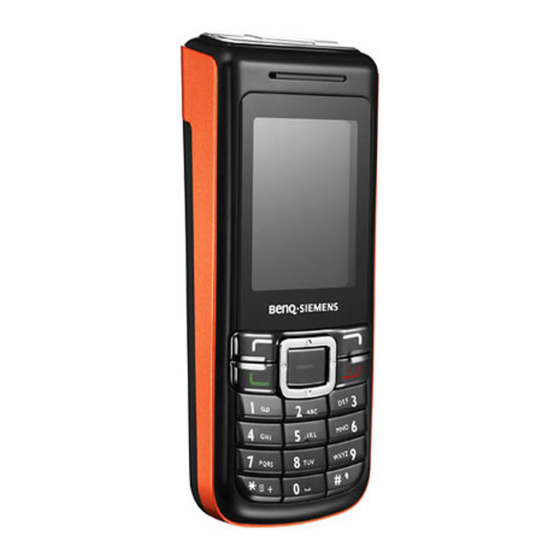
Summary of Contents for BENQ-SIEMENS E61
- Page 1 Release 1.0 Service Repair Documentation Level 3 - E61 Release Date Department Notes to change 12.05.2006 BenQ S CC CES New document R 1.0 06/2006 Technical Documentation TTD_Repair_L3 _Theory of Operation_E61_R1.0.pdf Page 1 of 33...
-
Page 2: Table Of Contents
Release 1.0 Table of Content Introduction ..........................3 ..........................3 URPOSE ...........................3 COPE ....................3 ERMS AND BBREVIATIONS List of available level 3 parts....................4 Required Equipment for Level 3 ....................6 Required Software for Level 3....................6 Radio Part ..........................7 ......................7 ECEIVER PERATION ......................8 RANSMITTER PERATION VCXO O .........................9... -
Page 3: Introduction
Release 1.0 1 Introduction 1.1 Purpose This Service Repair Documentation is intended to carry out repairs on BenQ repair level 3-4. 1.2 Scope This document is the reference document for all BenQ authorised Service Partners which are released to repair Siemens mobile phones up to level 3. 1.3 Terms and Abbreviations 06/2006 Technical Documentation... -
Page 4: List Of Available Level 3 Parts
Release 1.0 2 List of available level 3 parts Product ID Order Number Description CM L50634-Z97-C553 CONNDCPWRPA05302-QNJBQ2B.13120.021 SPCON L50634-Z97-C557 CONN24PD.4H1.5AXK824145YBQ2K.L1142.024 LCDM L50634-Z97-C562 CONN30PD5H185AXK5F30545YBQ2K.L1143.030 L50634-Z97-C668 CONNSKT24PD.4AXK724245BQ2K.L1165.024 BATC1 L50634-Z97-C664 CONNBATTCBE-3111-2769HBQ2K.N0079.011 BATC2 L50634-Z97-C665 CONNBATT2PJ-3111H-2-25BQ2K.N0079.071 L50634-Z97-C558 CONNI/O10PP0.5BQ2K.N0081.001 ANT1 L50634-Z97-C666 CONNSPRING2PN027M4-2I3BQ2K.N0082.031 KPCON L50634-Z97-C667 CONNBTB14PFBF05314BQNBQ2K.N1003.021 L50634-Z97-C659 CONNSIMCARDBM05106-L5BQ2K.N5030.021 MINISD L50634-Z97-C669... - Page 5 Release 1.0 LED7 L50640-L2179-D670 DISOPT19-213AUWD/S365-2BQ8C.19213.071 LED8 L50640-L2179-D670 DISOPT19-213AUWD/S365-2BQ8C.19213.071 LED9 L50640-L2179-D670 DISOPT19-213AUWD/S365-2BQ8C.19213.071 LED10 L50640-L2179-D670 DISOPT19-213AUWD/S365-2BQ8C.19213.071 L50640-D5123-D670 DISDIODERB161M-20BQ8C.1R002.08Q L50640-D5124-D670 DISDIODEPMEG2020EJBQ8C.2R002.A8F D601 L50640-D5124-D670 DISDIODEPMEG2020EJBQ8C.2R002.A8F DZB1 L50640-D3142-D670 DISDIODEZEN6.06-6.33VBQ8C.6R205.03F L50640-D5125-D670 DISDIODE1PS79SB30BQ8C.R2004.A84 L50640-D5125-D670 DISDIODE1PS79SB30BQ8C.R2004.A84 L50640-C2149-D670 DISTRANSPEMH9NPNBQ8D.00009.010 L50640-C2167-D670 DISTRANSUMH10NNPNBQ8D.00010.01F L50640-C2143-D670 DISTRANSBC807-40WPNPBQ8D.00807.A1K L50630-C1198-D670 DISTRANSFDG6303NBQ8D.06303.03K L50630-C1186-D670 DISTRANSFETFDC6306PBQ8D.06306.030 L50630-C1186-D670 DISTRANSFETFDC6306PBQ8D.06306.030 L50630-C1187-D670 DISTRANSFETFDC6506PBQ8D.06506.030 L50645-K280-Y420...
-
Page 6: Required Equipment For Level 3
L50645-F102-Y49 OSCCRYST32.768DST520BQ8B.33276.705 3 Required Equipment for Level 3 GSM-Tester PC-incl. Monitor, Keyboard and Mouse USB boot cable with USB foxlink driver (F30032-P601-A1) Troubleshooting Frame E61 Power Supply Spectrum Analyser Active RF-Probe incl. Power Supply Oscilloscope incl. Probe RF-Connector (N<>SMA(f)) Power Supply Cables... -
Page 7: Radio Part
Release 1.0 5 Radio Part 5.1 Receiver Operation IRxP GSM LNA IRxN RX GSM: 925~960 MHz GSM: 1850~1920 MHz Shift(1/2) DCS LNA DCS: ADC/DAC & Control Logic for DC Offset Cancellation 1805~1880 MHz Switch DCS: 1805~1880 MHz PCS: 1930~1990 MHz Shift(1/2) QRxP QRxN... -
Page 8: Transmitter Operation
Release 1.0 In addition, the base-band section integrates A/D and D/A converters which provide automatic on- chip correction of DC offsets. The three switched gain stages in each channel are DC coupled and provide 90dB gain control range with 2dB step size. The first PGA has a voltage gain range (x8-x1) with 6dB steps. -
Page 9: Vcxo Operation
Release 1.0 A secondary advantage of the OPLL is that the output signal, coming from a VCO, is truly constant envelope. This removes the problem of spectral spreading caused by AM to AM and AM to PM conversion in the power amplifier. The OPLL is formed from an on chip Gilbert cell down converter, limiter and phase detector with on chip passive loop filter. -
Page 10: Logic (Base-Band)
6 Logic (Base-Band) Introduction: E61 utilizes TI’s chipsets (CALYPSO and IOTA) and RENESAS’s chipset (SHJ2SLSL) as base- band solution. Base-band is composed with three potions: Logic, Analog/Codec and MMP. CALYPSO is a GSM/GPRS digital base-band logic solution included microprocessor, DSP, and peripherals. - Page 11 Release 1.0 IOTA 06/2006 Technical Documentation TTD_Repair_L3 _Theory of Operation_E61_R1.0.pdf Page 11 of 33...
-
Page 12: Calypso
In E61, we implement software flow control by only two signals: TXD0 and RXD0. General Purposes I/O (GPIO) Calypso provides 16 GPIOs configurable in read or write mode by internal registers. In E61, we utilize all of them as follows: IO0: Let MMP power-on reset;... - Page 13 It also provides 6 chip-select signals corresponding each to an address range of 8 mega bytes. One of these chip-select is dedicated to the selection of an internal memory. In E61, we employ nCS0/nCS1 (nCS0_NROM/nCS1_NROM) for external Flash and nCS2 (nCS2_NSRAM) for external SRAM.
- Page 14 The parallel interface allows control 13 external individual outputs and 1 internal signal with a time accuracy of the quarter of GSM bit. These parallel signals are mainly used to control the RF activity. In E61, we employ 7 of them to control RF activity. TSPACT1:...
-
Page 15: Iota
Release 1.0 6.2 IOTA Together with a digital base-band device (Calypso), IOTA is part of a TI DSP solution intended for digital cellular telephone applications including GSM 900, DCS 1800 and PCS 1900 standards (dual band capability). It includes a complete set of base-band functions to perform the interface and processing of voice signals, base-band in-phase (I) and quadrature (Q) signals which support single-slot and multi- slot mode, associated auxiliary RF control features, supply voltage regulation, battery charging control and switch ON/OFF system analysis. - Page 16 Release 1.0 Automatic Power Control (APC) Purpose of the Automatic Power Control (APC) is to generate an envelope signal to control the power ramping up, ramping down and power level of the radio burst. The APC structure is intended to support single slot and multi-slots transmission with smooth power transition when consecutive bursts are transmitted at different power level.
- Page 17 Release 1.0 SIM card shifters (SIMS) The SIM card digital interface in ABB insures the translation of logic levels between DBB and SIM card, for transmission of 3 different signals; a clock derived from a clock elaborated in DBB, to the SIM card (DBBSCK SIMCLK).
- Page 18 Release 1.0 Battery charger Interface (BCI) The main function of the ABB charger interface is the charging control of either a 1-cell Li-ion Battery or 3-serie Ni-MH cell batteries with the support of the micro-controller. The battery monitoring uses the 10 bit ADC converter from the MADC to measure the battery voltage, battery temperature, battery type, battery charge current, battery charger input voltage.
-
Page 19: Power Supply
Release 1.0 6.3 Power Supply V B A T A B B R S I M S I M V R S I M 1 .8 / 2 .9 V C A R D 1 0 m A R R A M S R A M V R R A M V C A M... -
Page 20: System Power On/Off Sequence
Release 1.0 Description: The voltage regulators embedded in IOTA consists of seven sub blocks. Several low-dropout (LDO) regulators perform linear voltage regulation. These regulators supply power to internal analog and digital circuit, to DBB processor, and to external memory. · LDO (VRDBB) is a programmable regulator that generates the supply voltages (1.8V,1.5V and 1.3V) for the core of the DBB processor. -
Page 21: Memory Circuit
Release 1.0 2. Check if Main Battery voltage is greater than 3.2V 3. Enable charge VRDBB-VRABB-VRMEM-VRRAM 4. Regulator OK. 5. ON_nOFF=1, ABB RSTz=1 6. NRESET pin is set from ‘L’ to ‘H’ 7. 13MHz clock oscillator is enabled Power off mode This state is reached when there is not enough voltage in the main battery and backup battery or when both batteries are disconnected. - Page 22 Release 1.0 Description: The two diagrams show the memory circuit of E61 and internal package connections for the Stacked CSP family with multiple die. The 128-Mbit 1.8 Volt Intel Wireless Flash Memory Stacked CSP Family encompass multiple flash memory + 32M bit RAM die combinations.
-
Page 23: Lcd Module (Lcdm)
Release 1.0 6.5 LCD module (LCDM) LCDM connector EMI2 LFA144 LCDM LCDM.DB15 DB15 LCDM.DB14 DB14 LED- LED- 5 SHD[0..15] G2/nLCDRST 8 SHD15 LCDM.DB13 DB13 LED+ LED+ 5 SHD14 J2SL/nLCDRST 7 SHD13 LCDM.DB12 DB12 EMI3 LFA144 SHD12 SHD11 LCDM.DB11 DB11 HW_LCM_ID HW_LCDM_ID 3,4 SHD10 SHD9... -
Page 24: Camera Module
Release 1.0 LCM Backlight LED driver schematic LED Driver SKT 33uH BLDRV VBAT BLM18RK102SN1 RB166 0 DAC/LIGHT_CTRL CTRL VOUT LED+ 11 LM3501 IO1/CSTN_LEDEN LED- 11 AGND LM3501 White LED Driv er 74.03501.040 BGND I_LED = ( 0.191 * Vctrl ) / R17 BGND LM3501 is a fixed operating frequency (1MHz) step-up DC/DC converter which can drive up to 3 white leds in series. -
Page 25: Interfaces
Release 1.0 The CM-5633 CMOS DSC module consists of COMS Sensor (OV7660) and Lens (Largon 923). The DSC module requires three different voltages of power supplies, which include VDSCA = 2.5V, DSCC = 1.8V and DOVDD = 2.8V. The DSC module is controlled by the J2SL, the multimedia processor, using the standard I2C control interface. -
Page 26: Multimedia Application Input Circuit Design
Release 1.0 The voice input used to audio codec microphone port transmission the voice signal. Microphone input path to handheld and hands-free application. The handheld used to differential input for main path. However hands-free used to signal input transmission voice the uplink path. 7.1.2 Multimedia Application Input Circuit Design The schematic provides audio codec input path circuit design, the two signal input used to voice... -
Page 27: Multimedia Application Output Circuit Design
Release 1.0 7.1.3 Multimedia Application Output Circuit Design 7.1.4 Loudspeaker output path and D-amplifier design The audio codec provides output path application, two mono output and one stereo output. A mono output use so d to differential signal applies to uplink voice output transfer IOTA produce. The OUT2 output used to differential signal for Loudspeaker function, but design addition the D amplifier for gain amplifier provides MP3 play, melody and speaker phone function the application .The stereo output supply to hands-free... -
Page 28: Pins I/Oconnector
Release 1.0 7.2 10 Pins I/O connector Pin No. Pin Definition Function description DC in/USB 5V External accessory power supply to the mobile phone DC out(default) Internal power provides for any powered accessory USB data - USB differential data line: D- USB data + USB differential data line: D+ UART Tx... -
Page 29: Mini-Sd Card
Release 1.0 Description The 10pin I/O Jack circuit is used for 4 kind of BenQ type accessory service: mono headset, stereo headset, UART data cable, and pure USB cable. Whenever the accessory plugs into the mobile, I/O 6 will be pull to low level. And then according to the difference resistance value mounted on the accessory, the system will get the difference ADC value from the EARPHONE_IN pin and recognize what type has plugged in. -
Page 30: Keypad Led Circuit
7.4 Keypad LED circuit Schematic Description E61 employs eight white LEDs for keypad backlight. When KEYLED sets to “L”, Keypad LEDs are turned on; otherwise the Keypad LEDs are turned off. The default VBATBB is 3.8 Volt. 7.5 Vibrator Schematic... -
Page 31: Keypad
Release 1.0 Description Vibrator is enabled by LEDB control logic in IOTA. When the logic is set to ‘H’, the motor will activate. RB54 and RB55 are used to control operating current and D1 is used to reduce EMF. Under the condition of VBAT = 3.8V, the average drain current is around 66.5mA. 7.6 Keypad Schematics 06/2006... - Page 32 Release 1.0 Description The keypad is made of a 5 Column x 5 Row matrixes. The keypad matrix is as follows: 06/2006 Technical Documentation TTD_Repair_L3 _Theory of Operation_E61_R1.0.pdf Page 32 of 33...
-
Page 33: Charging Circuit
Charging from USB Description E61 can charge the Li-ion/Li Polymer Battery from AC adaptor and USB, red line is the charging route from adaptor show the route of USB, red line is the charging route from USB. While USB and adaptor have plugged in at the same time, FP2 allows charging only from adaptor.
Need help?
Do you have a question about the E61 and is the answer not in the manual?
Questions and answers