Table of Contents
Advertisement
Quick Links
Notes: Please refer to the Original Service Manual for :
CD Mechanism Unit, Order No. PSG1303059AE
Speaker system SB-PMX100EGK, Order No. PSG1505005CE
TABLE OF CONTENTS
1 Safety Precautions----------------------------------------------- 3
1.1. General Guidelines---------------------------------------- 3
1.2. Before Repair and Adjustment ------------------------- 4
1.3. Protection Circuitry ---------------------------------------- 4
1.4. Caution For Fuse Replacement------------------------ 4
1.5. Safety Part Information----------------------------------- 4
Model No.
Product Color: (S)...Silver Type
PAGE
2 Warning --------------------------------------------------------------5
to Electrostatically Sensitive (ES) Devices ----------5
2.2. Precaution of Laser Diode -------------------------------5
2.4. Handling Precaution for Traverse Unit----------------6
© Panasonic Corporation 2015. All rights reserved.
Unauthorized copying and distribution is a violation of
law.
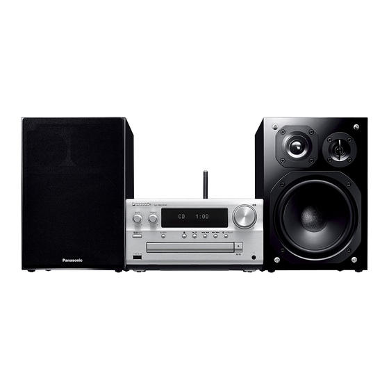
CD Stereo System
SA-PMX100EG
PSG1505004CE
PAGE
Advertisement
Table of Contents

Related Manuals for Panasonic SA-PMX100EG


Summary of Contents for Panasonic SA-PMX100EG
-
Page 1: Table Of Contents
1.4. Caution For Fuse Replacement------------------------ 4 2.3. Service caution based on Legal restrictions --------6 1.5. Safety Part Information----------------------------------- 4 2.4. Handling Precaution for Traverse Unit----------------6 © Panasonic Corporation 2015. All rights reserved. Unauthorized copying and distribution is a violation of law. - Page 2 3 Service Navigation------------------------------------------------8 13.3. PANEL, IR SENSOR & HEADPHONE P.C.B.---- 62 3.1. Service Information ----------------------------------------8 13.4. SMPS P.C.B.---------------------------------------------- 63 14 Voltage Measurement ----------------------------------------- 65 4 Specifications ------------------------------------------------------9 5 Location of Controls and Components------------------ 10 14.1. MAIN (SUPPLY) P.C.B. -------------------------------- 65 5.1.
-
Page 3: Safety Precautions
1 Safety Precautions 1.1. General Guidelines 1. IMPORTANT SAFETY NOTICE There are special components used in this equipment which are important for safety. These parts are marked by in the Schematic Diagrams, Circuit Board Layout, Exploded Views and Replacement Parts List. It is essential that these critical parts should be replaced with manufacturer’s specified parts to prevent X-RADIATION, shock, fire, or other hazards. -
Page 4: Before Repair And Adjustment
1.2. Before Repair and Adjustment Disconnect AC power & discharge AC Capacitors (C5700, C5701, C5702, C5705 and C5706) through a 10W, 1W resistor to ground. Caution : DO NOT SHORT-CIRCUIT DIRECTLY (with a screwdriver blade, for instance), as this may destroy solid state devices. After repairs are completed, restore power gradually using a variac, to avoid overcurrent. -
Page 5: Warning
2 Warning 2.1. Prevention of Electrostatic Discharge (ESD) to Electrostatically Sensi- tive (ES) Devices Some semiconductor (solid state) devices can be damaged easily by static electricity. Such components commonly are called Elec- trostatically Sensitive (ES) Devices. The following techniques should be used to help reduce the incidence of component damage caused by electrostatic discharge (ESD). -
Page 6: Service Caution Based On Legal Restrictions
Maximale Strahlungsleistung der Lasereinheit :100 μW/VDE Die Strahlung an der Lasereinheit ist ungefährlich, wenn folgende Punkte beachtet werden: 1. Die Lasereinheit nicht zerlegen, da die Strahlung an der freigelegten Laserdiode gefährlich ist. 2. Den werkseitig justierten Einstellregler der Lasereinhit nicht verstellen. 3. - Page 7 2. To prevent the laser diode from the electrostatic discharge damage, the flexible cable of the optical pickup unit removed should be short-circuited with a short pin or a clip. 3. The flexible cable may be cut off if an excessive force is applied to it. Use caution when handling the flexible cable. 4.
-
Page 8: Service Navigation
3 Service Navigation 3.1. Service Information This service manual contains technical information which will allow service personnel’s to understand and service this model. Please place orders using the parts list and not the drawing reference numbers. If the circuit is changed or modified, this information will be followed by supplement service manual to be filed with original service manual. -
Page 9: Specifications
4 Specifications Speaker unit(s) Woofer 14 cm cone type x 1 Tweeter 1.9 cm dome type x 1 Super tweeter 1.2 cm piezoelectric type x 1 General 3 Ω Impedance Power supply AC 220 V to 240 V, 50 Hz Dimensions (W x H x D) 161 mm x 238 mm x 264 mm Power consumption... -
Page 10: Location Of Controls And Components
5 Location of Controls and Components 5.1. Main Unit & Remote Control Key Button Operations... -
Page 11: Service Mode
6 Service Mode This unit is equipped with features of self diagnostic & doctor mode setting for checking the functions & reliability. 6.1. Service Mode Table Item FL display Key operation Mode name Description Step 1 : Select CD mode Service Mode To enter into Service Mode (Ensure no disc is inserted). -
Page 12: Service Mode Error Code
6.2. Service Mode Error Code 6.2.1. CD Mechanism Error Code Table Error Code Diagnostic Contents Description of error Automatic FL Display Remarks During normal operation, if CD H15 CD Closing Abnormal Press [ ] on main unit for “POS_SW_R (OPEN_SW)” next error. -
Page 13: Doctor Mode
6.3. Doctor Mode 6.3.1. Doctor Mode Table 1 Item Key Operation FL Display Front Key Mode Name Description To enter into Doctor Mode for In any mode: Doctor Mode (Display 1) checking of various items and Press button on main unit follow by displaying EEPROM check sum [4] &... - Page 14 6.3.2. Doctor Mode Table 2 Item Key Operation FL Display Front Key Mode Name Description CD Traverse To check for the traverse unit In Doctor Mode: Test Mode operation. In this mode, the Press [ ] follow by [1] & then [2] first &...
- Page 15 6.3.3. Doctor Mode Table 3 Item Key Operation FL Display Front Key Mode Name Description Bluetooth Mac Bluetooth Address Check In Doctor Mode: Address Checking Select to the Bluetooth Mode Press [ ] follow by [3] & then [1] button on the remote control. Display of Bluetooth MAC Address will To cancel, press [0] button on remote scroll forever...
-
Page 16: Sales Demonstration Lock Function Mode
6.4. Sales Demonstration Lock Function Mode Item Key Operation FL Display Front Key Mode Name Description Sales Demo Mainly used when the system Step 1 : Turn on the unit. is in display at sales division Step 2 : Press and hold [OPEN/CLOSE] and [SELECTOR] keys for 5 secs. -
Page 17: Troubleshooting Guide
7 Troubleshooting Guide 7.1. No Power No power during power-on of the unit Table1 SMPS H2015 -MAIN CN1100) Pin No. Voltage Value Confirmation if AC Power from SMPS P.C.B. to Main P.C.B. Is AC Power present at the AC Inlet (P5701) ? Check AC Cord and AC Inlet &... -
Page 18: No Connection For Airplay And Allplay Group
7.3. No connection for AirPlay and AllPlay group Table3 Pin CN8020 (CN8010 Pin No. Voltage Value No AirPlay and AllPlay connection Check network connection and connection setting on smart phone or tablet. (refer to user’s manual) Table3 Is terminal voltage between CN8020 (Relay) and CN8010 (Main) OK? Replace 24P wire Is 24P wire between CN8020 (Relay) and CN8010 (Main) OK? Table4... -
Page 19: Disassembly And Assembly Instructions
8 Disassembly and Assembly Instructions Caution Note: • This section describes the disassembly and/or assembly procedures for all major printed circuit boards & main compo- nents for the unit. (You may refer to the section of “Main components and P.C.B Locations” as described in this service manual) •... -
Page 20: Disassembly Flow Chart
8.1. Disassembly flow chart The following chart is the procedure for disassembling the casing and inside parts for internal inspection when carrying out the ser- vicing. To assemble the unit, reverse the steps shown in the chart below. 8.2. Type of screws... -
Page 21: Main Parts Location Diagram
8.3. Main Parts Location Diagram... -
Page 22: Disassembly Of Top Cabinet
8.4. Disassembly of Top Cabinet Step 4 : Lift up to remove Top Cabinet. Step 1 : Remove 2 screws. Step 2 : Remove 3 screws. Step 3 : Adjust Dipole Antenna. -
Page 23: Disassembly Of Relay Block
8.5. Disassembly of Relay Block Step 3 : Remove 2 screws and detach ground wire. Step 4 : Remove screw. • Refer to “Disassembly of Top Cabinet” Step 5 : Detach antenna wire at connector (J2) on ALLPLAY Module. Step 1 : Remove 5 screws. Step 2 : Push inwards Dipole Antenna. - Page 24 Step 6 : Detach 7P wire at connector (CN8254) on Relay Step 9 : Release guide. P.C.B.. Step 10 : Lift up and remove Relay Block. Step 7 : Release 7P wire through groove at Support P.C.B.. Step 8 : Detach 24P FFC at connector (CN8020) on Relay P.C.B..
- Page 25 Caution : During assembling, insert the Relay Block & 8.5.1. Disassembly of Dipole Antenna ensure seated onto the guides. • Refer to “Disassembly of Top Cabinet” • Refer to “Disassembly of Relay Block” Step 1 : Release antenna wire from the groove. Step 2 : Detach antenna wire at connector (Ant1) on ALLPLAY Module.
-
Page 26: Disassembly Of Front Panel Unit
8.5.3. Disassembly of Relay P.C.B. 8.6. Disassembly of Front Panel • Refer to “Disassembly of Top Cabinet” Unit • Refer to “Disassembly of Relay Block” • Refer to “Disassembly of Top Cabinet” Step 1 : Release antenna wire from the groove. Step 1 : Remove 2 screws and detach ground wire. -
Page 27: Disassembly Of Panel Block
Step 6 : Release tabs on both sides of Front Panel Unit. Step 9 : Insert flathead screwdriver into both gaps. Step 7 : Press to release catches. Step 10 : Apply light force at both gaps to lift up Front Panel Step 8 : Slightly lift forward Front Panel Unit. - Page 28 Step 4 : Release wires from the guide. 8.7.2. Disassembly of Headphone P.C.B. Step 5 : Remove 4 screws. Step 1 : Release ground wire from slot. Step 6 : Release catches. Step 2 : Remove Headphone P.C.B.. Step 7 : Remove Panel Block. 8.7.3.
-
Page 29: Disassembly Of Usb P.c.b
8.8. Disassembly of USB P.C.B. 8.9. Disassembly of Antenna P.C.B. • Refer to “Disassembly of Top Cabinet” • Refer to “Disassembly of Top Cabinet” • Refer to “Disassembly of Front Panel Unit” • Refer to “Disassembly of Front Panel Unit” •... -
Page 30: Disassembly Of Smps P.c.b
8.10. Disassembly of SMPS P.C.B. 8.11. Disassembly of Main P.C.B. • Refer to “Disassembly of Top Cabinet” • Refer to “Disassembly of Top Cabinet” • Refer to “Disassembly of Relay Block” Step 1 : Detach 15P Wire at connector (CN1100) on Main •... -
Page 31: Disassembly Of Inner Chassis
8.12. Disassembly of Inner Chassis Step 2 : Remove 2 screws. Step 3 : Lift up to release Inner Chassis from Rear Cabinet. • Refer to “Disassembly of Top Cabinet” Caution : During assembling, ensure the Inner Chassis is • Refer to “Disassembly of Relay Block” fully inserted &... -
Page 32: Disassembly Of Tuner P.c.b
8.13. Disassembly of Tuner P.C.B. 8.14. Disassembly of CD Mecha- nism Unit • Refer to “Disassembly of Top Cabinet” • Refer to “Disassembly of Relay Block” • Refer to “Disassembly of Top Cabinet” • Refer to “Disassembly of Front Panel Unit” •... -
Page 33: Replacement Of Traverse Unit
8.15. Replacement of Traverse Unit Step 2 : Slide tray out fully. • Refer to “Disassembly of CD Mechanism Unit” 8.15.1. Disassembly of Traverse Unit Caution : Refer to “2.4 Handling Precaution for Traverse Unit” to prevent static damage to the Optical Pickup Unit. Note: 1. - Page 34 Step 4 : Release the guide as shown & slide Traverse Slide Step 6 : Lift up Traverse Unit by approximately 45°. Plate to the end. Step 7 : Remove traverse unit as arrow shown. Step 5 : Detach 5P FFC at the connector (CN7001) on CD Interface P.C.B..
- Page 35 Caution : Avoid touching the surface of the Optical Pickup Step 2 : Insert Traverse Unit at approximately 45° into mecha Unit on the traverse unit. unit as arrow shown. 8.15.2. Assembly of Traverse Unit Step 1 : Release the guide as shown & slide Traverse Slide Plate to the end.
- Page 36 Step 3 : Insert Traverse Unit properly into the grooves. Step 4 : Slide Traverse Slide Plate to lock the Traverse Unit as shown. Step 5 : Connect 5P FFC at connector (CN7001) on CD Inter- face P.C.B.. Step 6 : Slide Traverse Slide Plate until it stop at the guide.
- Page 37 Step 7 : Align and insert the tray into the mecha unit. Step 9 : Slide the tray in fully. Step 8 : Align the guides of the Traverse Slide Plate with the grooves when sliding the tray in.
- Page 38 8.15.3. Disassembly of CD Interface P.C.B. Step 2 : Remove 2 screws. Step 3 : Attach short pin to Traverse Unit. • Refer to “Disassembly of CD Mechanism Unit” • Refer to “Disassembly of Traverse Unit” Note : The circuit is to be short to prevent electrostatic dis- charge during replacement of CD Interface P.C.B..
-
Page 39: Disassembly Of Bluetooth P.c.b
8.16. Disassembly of Bluetooth 8.17. Disassembly of Rear Cabinet P.C.B. • Refer to “Disassembly of Top Cabinet” • Refer to “Disassembly of Relay Block” • Refer to “Disassembly of Top Cabinet” • Refer to “Disassembly of Front Panel Unit” • Refer to “Disassembly of Relay Block” •... -
Page 40: Service Position
9 Service Position Note: For description of the disassembly procedures, see the Section 8 9.1. Checking of Panel Block, Step 8 : Place Antenna P.C.B. on an Insulated Material. Step 9 : Connect antenna wire at connector (J2) on ALLPLAY Relay, Antenna P.C.B. -
Page 41: Checking Of Smps P.c.b
9.2. Checking of SMPS P.C.B. Step 9 : Place Antenna P.C.B. on an Insulated Material. Step 10 : Connect antenna wire at connector (J2) on ALLPLAY Module. Step 1 : Remove Top Cabinet. Step 2 : Remove Front Panel Unit. Step 3 : Remove Panel Block. -
Page 42: Checking Of Main P.c.b
Step 11 : Place SMPS P.C.B. on an Insulated Material. 9.3. Checking of Main P.C.B. Step 12 : Connect 15P wire at the connector (CN1100) on the Main P.C.B.. Step 1 : Remove Top Cabinet. Step 13 : Check SMPS P.C.B. according to the diagram shown. Step 2 : Remove Front Panel Unit. - Page 43 Step 15 : Place CD Mechanism Unit on an insulated material. Step 16 : Connect 10P FFC at connector (CN5001) on Main P.C.B.. Step 17 : Connect 24P FFC at connector (CN5002) on Main P.C.B.. Step 18 : Check Main according to the diagram shown.
-
Page 45: Block Diagram
USB_5V CN7001 OPEN_SW OPEN_SW CN7002 CN5001 OPEN_SW CN8012 CN6005 CN6000 CN6100 OPEN_SW USB PORT USB_D+ 98 DP_OUT DP_IN 10 USB_D+ CN8012 CN6005 CN6000 CN6100 USB_D- 97 DM_OUT DM_IN 11 USB_D- CD INTERFACE P.C.B. SA-PMX100EG SERVO & SYSTEM CONTROL BLOCK DIAGRAM... -
Page 46: Audio Block Diagram
VALID 24 7 RST_AB BST_C D4200 17 RST_CD DSP_SCL XI 41 CN4200 OUT_C X4100 RIGHT D8000 DSP_SDA CN4200 XO 42 OUT_D BST_D DAMP_VALID DAMP_MUTE DAMP_OTW 2 OTW DC DETECT +24V CIRCUIT DAMP_SD 5 SD Q4200,Q4201 Q4202,Q4203 DC_DET_DAMP SA-PMX100EG AUDIO BLOCK DIAGRAM... -
Page 47: Power Supply (1/2) Block Diagram
FB 4 DAMPVDD_24V H2015 CN1100 DAMPVDD_24V DAMPVDD_24V +24V M_VDET PC5721 PCONT FROM FEEDBACK SMPS_STOP SMPS_STOP H2015 CN1100 SMPS_STOP SERVO & SYSTEM CONTROL FEEDBACK CIRCUIT ECO_CTL H2015 CN1100 ECO_CTL ECO_CTL IC5801 SHUNT REGULATOR Q5863,Q5864 PRIMARY SECONDARY SA-PMX100EG POWER SUPPLY (1/2) BLOCK DIAGRAM... -
Page 48: Power Supply (2/2) Block Diagram
PW_D3R3V PW_D3R3V CN8001 CN9200 PW_D3R3V PW_D3R3V CN9201 CN4000 PW_D3R3V PW_D3R3V +3.3V TUNER P.C.B. PW_D3R3V CN8008 CN51 PW_D3R3V PW_3DR3V +3.3V TO POWER SUPPLY RELAY P.C.B. BLOCK (1/2) PW_3.3V_MR PW_3.3V_MR PW_3.3V_MR CN8010 CN8020 +3.3V 17,19,22,23,24 1,2,3,6,8 SA-PMX100EG POWER SUPPLY (2/2) BLOCK DIAGRAM... -
Page 49: Wiring Connection Diagram
CN8012 CN4201 ZJ920 CN8022 CN8254 CN8021 CN1100 RELAY P.C.B. HEADPHONE P.C.B. CN8020 P8001 P8000 ZJ9200 CN9202 NFC P.C.B. H2015 PANEL P.C.B. PANEL P.C.B. P5701 SMPS P.C.B. CN4000 AC IN 220V ~ 240V 60Hz CN9201 P9200 CN9200 SA-PMX100EG WIRING CONNECTION DIAGRAM... -
Page 51: Schematic Diagram
12 Schematic Diagram 12.1. Schematic Diagram Notes • Voltage and signal line (All schematic diagrams may be modified at any time with : +B Signal Line the development of new technology) : Aux / Tuner Signal Line Notes: S7201: RESET switch. : Audio Signal Line S9203: REW switch (... -
Page 53: Cd Interface, Tuner, Usb & Antenna Circuit
2.2K FM ANT TUN_BCK TO MAIN P.C.B. RFGND DOUT TUN_DATA THERMAL (CN8008) LB51 VA51 DGND J0JYC0000656 B0ZBZ0000156 PW_3R3V SDIO SCLK RESET NOTE: “ * ” REF IS FOR INDICATION ONLY SA-PMX100EG CD INTERFACE / TUNER / USB / ANTENNA CIRCUIT... -
Page 54: Relay Circuit (1/2)
PW_3R3V_MR TO ALLPLAY MODULE SPI_CS MR_GPIO04 R8316 SDTO MR_MCLK(I2S) R8270 R8272 MR_BCK(I2S) TO RELAY CIRCUIT (2/2) R8273 MR_LRCK(I2S) NXP_SEL R8327 R8310 MR_DATAIN(I2S) R8274 MR_DATAOUT(I2S) PW_3R3V_MR ALL_SDATA R8269 C8315 USB_DATA_DPM IC8106 USBDATA_DPP C0JBAZ001876 QUAD INVERTER ALL_LRCK R8271 ALL_BCLK SA-PMX100EG RELAY CIRCUIT... -
Page 55: Relay Circuit (2/2)
C8289 VDDIO [36] P6_0 [73] CN8253 C8308 C8307 C8306 P0_0 VDDIO R8293 TRST P4_9 VSSIO R8290 C8296 P0_1 P2_0 SOFTWARE C8292 DOWNLOAD C8304 3R3V 52 53 65 66 67 RESET C8288 C8297 C8293 TO RELAY CIRCUIT (1/2) SA-PMX100EG RELAY CIRCUIT... -
Page 56: Panel Circuit
STOP SELECTOR TREBLE HP_GND BASS IN SCHEMATIC HP_DET DIAGRAM - 5 SMPS GND 1 2 3 1 2 3 C9210 C9214 C9211 C9215 100P 100P 100P 100P R9203 R9205 R9204 R9206 TRE_JOGA BAS_JOGA PW_STBY3V3 PW_STBY3V3 BAS_JOGB TRE_JOGB SA-PMX100EG PANEL CIRCUIT... -
Page 57: Ir Sensor & Headphone Circuit
JK8000 LB8001 J0JGC0000070 P8000 R8001 C8001 LB8002 HP_GND PANEL CIRCUIT C8004 R8000 C8000 HEADPHONE (CN9202) LB8000 HP_GND J0JGC0000070 IN SCHEMATIC HP_DET DIAGRAM - 4 SMPS GND P8001 C8003 SMPS GND CHASSIS GND SMPS GND SA-PMX100EG IR SENSOR / HEADPHONE CIRCUIT... -
Page 58: Smps Circuit (1/2)
B1ABGC000001 SWITCH R5809 1.5K R5868 C5870 R5801 C5817 R5802 R5810 6800P R5814 R5804 R5806 100K C5820 1000P C5818 R5819 R5805 IC5801 R5728 C5819 R5817 C0DAAYY00072 2.2K C5828 SHUNT REGULATOR R5818 6.3V100 R5861 C5869 100K Q5863 B1ABGC000001 SWITCH SA-PMX100EG SMPS CIRCUIT... -
Page 59: Smps Circuit (2/2)
C5724 100P R5732 C5722 D5707 R5733 DZ2W22000L 1000P R5766 FB/OLP IC5701 D5713 C5730 C0DAAYY00064 DZ2J30000L R5727 C5747 SWITCHING REGULATOR S/OCP 0.13 470P PC5761 FEEDBACK PC5721 FEEDBACK R5808 4.7K NOTE: “ * ” REF IS FOR INDICATION ONLY SA-PMX100EG SMPS CIRCUIT... -
Page 60: Printed Circuit Board
3860AE 3860AE (SIDE A) (SIDE B) P8000 (TO ANTENNA) P8001* (TO CHASSIS GND) (SIDE A) (SIDE B) 3860AF 3860AF 3860AF 3860AF SA-PMX100EG CD INTERFACE / TUNER / USB / ANTENNA P.C.B. NOTE: " * " REF IS FOR INDICATION ONLY... -
Page 61: Relay P.c.b
37 40 7072 C8307 C8315 CN6004 C8306 C8308 CN8021 (TO ALLPLAY MODULE) CN8253 C8303 CN8020 3842A 3842A 3842A 3842A (TO MAIN P.C.B.) (FOR SOFTWARE DOWNLOAD) (SIDE A) (SIDE B) SA-PMX100EG RELAY P.C.B. NOTE: " * " REF IS FOR INDICATION ONLY... -
Page 62: Panel, Ir Sensor & Headphone P.c.b
ZJ920 C920 R920 P8001 R921 LB8000 (TO CHASSIS R8000 GND) IR921 C8000 C8003 SENSOR JK8000 C8004 C8001 3834AC 3834AC 3834AD 3834AD P8000 HEADPHONE SA-PMX100EG PANEL / IR SENSOR / HEADPHONE P.C.B. NOTE: " * " REF IS FOR INDICATION ONLY... -
Page 63: Smps P.c.b
R5720 C5701 R5864 ZA2* T5701 QR5862 (HEATSINK) C5791 R5862 (TRANSFORMER) 3834AA 3834AA CAUTION RISK OF ELECTRIC SHOCK AC VOLTAGE LINE. PRIMARY SECONDARY PLEASE DO NOT TOUCH THIS P.C.B SA-PMX100EG NOTE: " * " REF IS FOR INDICATION ONLY SMPS P.C.B. -
Page 65: Voltage Measurement
MODE POWER ON 0.98 REF NO. IC1102 MODE POWER ON 0.96 IC1104 REF NO. MODE POWER ON REF NO. IC1106 MODE POWER ON IC1107 REF NO. MODE POWER ON 1.55 IC1110 REF NO. MODE POWER ON SA-PMX100EG MAIN (SUPPLY) P.C.B. -
Page 66: Smps P.c.b
IC5822 REF NO. MODE POWER ON IC5823 REF NO. MODE POWER ON Q5760 Q5761 Q5863 Q5864 Q5720 REF NO. MODE POWER ON STANDBY REF NO. QR5762 QR5822 QR5823 QR5862 MODE POWER ON 12.9 12.9 STANDBY 12.9 12.9 SA-PMX100EG SMPS P.C.B. -
Page 67: Exploded View And Replacement Parts List
(ANTENNA P.C.B.) ZJ9200 (IR SENSOR P.C.B.) *CN7230 H2015 *P8001 ZJ5703 ZJ920 P8001 P8000 P8000 JK8000 IR921 (HEADPHONE (MECHANISM UNIT) P.C.B.) (CD INTERFACE S7201 P.C.B.) CN7002 SA-PMX100EG CN7001 NOTE: " * " PART IS NOT SUPPLIED/REF IS FOR INDICATION ONLY. CABINET DRAWING... -
Page 68: Packaging
15.2. Packaging ACCESSORIES BAG REMOTE CONTROL AC CORD SA-PMX100EG O/I BOOK FM INDOOR ANTENNA SB-PMX100EG A5 x 2 SPEAKER CABLE POLYFOAM (LEFT) F R O N POLYFOAM (RIGHT) SC-PMX100EG PACKAGING DRAWING... -
Page 69: Mechanical Replacement Parts List
15.3. Mechanical Replacement Parts List Safety Ref. No. Part No. Part Name & Qty Remarks Description Safety Ref. No. Part No. Part Name & Qty Remarks RMK0812-1 BOTTOM CHASSIS Description RMK0898 INNER CHASSIS RMQ2423 PC SHEET CABINET AND RMQ2463 SMPS PC SHEET CHASSIS RMQX0382-3 CD MECHA SUPPORT 2... - Page 70 Safety Ref. No. Part No. Part Name & Qty Remarks Description RFKKMX100EGS TOP AL ORNAMENT ASS’Y RGQ0748-K ANTENNA HOLDER RHD20024-1 SCREW RMF0587 HIMELON RMN1112 RELAY BRACKET N1CYYYY00012 DIPOLE ANTENNA REE1959 20P FFC (MAIN- WIFI MODULE) REE1960 30P FFC (MAIN- WIFI MODULE) RMF0519 HIMELON RMF0796...
-
Page 71: Electrical Replacement Parts List
15.4. Electrical Replacement Parts List Safety Ref. No. Part No. Part Name & Qty Remarks Description Safety Ref. No. Part No. Part Name & Qty Remarks IC8202 C1CB00004388 (E.S.D) Description TRANSISTORS PRINTED CIRCUIT BOARDS Q5720 B1BABG000007 TRANSISTOR (E.S.D) Q5760 B1ADCF000001 TRANSISTOR (E.S.D) PCB1... - Page 72 Safety Ref. No. Part No. Part Name & Qty Remarks Safety Ref. No. Part No. Part Name & Qty Remarks Description Description TRANSFORMERS DZ5701 D4EAY5110006 SURGE ABSORBER T5701 G4DYZ0000080 SWITCHING TRANS- FORMER VARIABLE RESIS- TORS PHOTO COUPLERS VR9200 EVEKE2F3024B VOLUME JOG PC5721 B3PBA0000579 PHOTO COUPLER...
- Page 73 Safety Ref. No. Part No. Part Name & Qty Remarks Safety Ref. No. Part No. Part Name & Qty Remarks Description Description D0GBR00J0004 1/10W R8292 D0GAR00J0005 1/16W R920 D0GB470JA065 1/10W R8293 D0GDR00J0004 1/8W R921 D0GB101JA065 1/10W R8294 D0GA101JA023 1/16W R2905 D1BB4701A074 4.7K 1/10W...
- Page 74 Safety Ref. No. Part No. Part Name & Qty Remarks Safety Ref. No. Part No. Part Name & Qty Remarks Description Description CAPACITORS C8304 F1G1C104A146 0.1uF C8305 F1G1C104A146 0.1uF F1H1H102B047 1000pF C8306 F1H0J1060006 10uF 6.3V F1G1C104A146 0.1uF C8307 F1H0J1060006 10uF 6.3V F1G1C104A146 0.1uF...
Need help?
Do you have a question about the SA-PMX100EG and is the answer not in the manual?
Questions and answers