Denon S-81 Service Manual
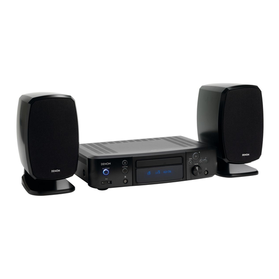
Personal audio system
Hide thumbs
Also See for S-81:
- Operating instructions manual (36 pages) ,
- Instrucciones de funcionamiento (36 pages) ,
- Code list (3 pages)
Table of Contents
Advertisement
Quick Links
For purposes of improvement, specifications and
●
design are subject to change without notice.
Please use this service manual with referring to the
●
operating instructions without fail.
Some illustrations using in this service manual are
●
slightly different from the actual set.
SERVICE MANUAL
MODEL
PERSONAL AUDIO SYSTEM
TOKYO, JAPAN
Denon Brand Company, D&M Holdings Inc.
For U.S.A., Canada, Europe,
U.K. & Japan model
S-81
S-81DAB
注 意
サービスをおこなう前に、このサービスマニュアルを
必ずお読みください。本機は、火災、感電、けがなど
に対する安全性を確保するために、さまざまな配慮を
おこなっており、また法的には「電気用品安全法」に
もとづき、所定の許可を得て製造されております。
従ってサービスをおこなう際は、これらの安全性が維
持されるよう、このサービスマニュアルに記載されて
いる注意事項を必ずお守りください。
本機の仕様は性能改良のため、予告なく変更すること
●
があります。
補修用性能部品の保有期間は、製造打切後8年です。
●
修理の際は、必ず取扱説明書を参照の上、作業を行っ
●
てください。
本文中に使用しているイラストは、説明の都合上現物
●
と多少異なる場合があります。
Ver. 4
Please refer to the
MODIFICATION NOTICE.
X0275V.04 DE/CDM 0611
Advertisement
Table of Contents

Related Manuals for Denon S-81


Summary of Contents for Denon S-81
- Page 1 Please use this service manual with referring to the ● 修理の際は、必ず取扱説明書を参照の上、作業を行っ ● operating instructions without fail. てください。 Some illustrations using in this service manual are ● 本文中に使用しているイラストは、説明の都合上現物 ● slightly different from the actual set. と多少異なる場合があります。 TOKYO, JAPAN Denon Brand Company, D&M Holdings Inc. X0275V.04 DE/CDM 0611...
-
Page 2: Safety Precautions
S-81/S-81DAB SAFETY PRECAUTIONS The following check should be performed for the continued protection of the customer and service technician. LEAKAGE CURRENT CHECK Before returning the unit to the customer, make sure you make either (1) a leakage current check or (2) a line to chassis resistance check. -
Page 3: Caution In Servicing
S-81/S-81DAB CAUTION IN SERVICING サービス時の注意事項 Initializing S-81/S-81DAB 本機の初期化について S-81/S-81DAB initialization should be performed when the µcom マイコンやマイコン周辺部品を交換した場合は、本機の初期化 and peripheral parts of µcom are replaced. を行って下さい。 1. Switch off the unit and remove the AC cord from the wall out- 1. 電源ボタンを押してスタンバイ状態にしてから、壁の電源... - Page 4 S-81/S-81DAB DISASSEMBLY 各部のはずしかた (Follow the procedure below in reverse order when (組み立てるときは、逆の順序でおこなってください。 ) reassembling.) 1. Loader Panel 1. ローダーパネルのはずしかた (1) Switch on, and press [ (OPEN/CLOSE)] button (1) 電源を入れ「 (OPEN/CLOSE)」ボタンを押して、 to open the Disc tray. (Refer to Fig. 1) ディスクトレイを開きます。(Fig.1 参照 ) When a power supply is not turned on, insert a stick etc.
- Page 5 S-81/S-81DAB 2. Top Cover 2. トップカバーのはずしかた (1) Remove 4 screws ① from the both sides. (1) 両サイドから①のネジ 4 本をはずします。 (2) Remove 6 screws ② from the Rear Panel, then de- (2) リアパネルから②のネジ 6 本をはずし、トップカ tach the Top Cover to the arrow direction.
- Page 6 S-81/S-81DAB 4. Rear Panel 4. リアパネルのはずしかた (1) Disconnect the connector of AC cord, and detach (1) AC コードのコネクタとコードブッシュをはずし the cord bushing. ます。 (2) Remove 3 ( or 5 in the case of U.S.A. & Canada (2) ⑥のネジ 3 本 (U.S.A. & Canada モデルの場合 :5 model ) screw ⑥...
- Page 7 S-81/S-81DAB 5. CD Mecha. Unit 5. CD メカユニットのはずしかた (1) Open the Tray completely by turning the gear under (1) メカユニットの下のギアを反時計方向に回して、 the Mecha. Unit counterclockwise. トレイを完全に開きます。 (2) Remove 2 screws ⑧ on the Tray’s hole. (2) トレイの孔から⑧のネジ 2 本をはずします。 (3) Remove 2 rear screws ⑨ fixing the CD Mecha.
- Page 8 S-81/S-81DAB BLOCK DIAGRAM...
-
Page 9: Level Diagram
S-81/S-81DAB LEVEL DIAGRAM... -
Page 10: Cd Test Mode
S-81/S-81DAB CD TEST MODE CD テストモード Button name Function Display キー名称 機能 表示 ・ 本体 STOP ボタンと ボタンを同時に押しなが Plug AC cord into power outlet while pressing the ・ ら、AC コードをコンセントへ接続する . STOP button and the button same time Version No. of on Main Unit. - Page 11 S-81/S-81DAB キー名称 機能 表示 Function Display Button name CD MPU : writing counter (from 000 to 100) CD の場合 :*** :書き込みカウンタ (% 表示:0 ∼ 100) Version Up mode ・When completing data writing VERSION UP モード ・書き込み終了時 Main MPU : ****** : SYSTEM : ****** : CD メインマイコンの場合:******:SYSTEM...
- Page 12 S-81/S-81DAB Function Display Button name キー名称 機能 表示 Continue S6 display ・ Press the CD OPEN/CLOSE button to open the ・CD OPEN/CLOSE ボタンでトレイを開く. S6 の表示を継続する. tray. ・ディスクを置き、再度 CD OPEN/CLOSE ボタンでトレイ ・ Set a disc on the tray, then press the CD OPEN/ を閉じるとディスクをチャッキングする....
- Page 13 S-81/S-81DAB Function Display Button name キー名称 機能 表示 When the the FUNCTION button is pressed for ・ flashing ・ ・FUNCTION ボタンを押す(2秒以上の長押しで ・ を点滅 under 2 seconds, the adjustment values are ① ない)と、下記の順番で調整値を表示する. ① displayed in the following order. ① FOCUS BALANCE FOCUS BALANCE ①...
- Page 14 S-81/S-81DAB Function Display Button name キー名称 機能 表示 The CD heat run mode is launched. Once writing ・ ・ ・CD ヒートランモードが起動し、TOC READ が完了し ・ を点灯 of the TOC data is completed, press the CD ① , ② た後、CD PLAY/PAUSE ボタンを押す.この時、...
- Page 15 S-81/S-81DAB Function Display Button name キー名称 機能 表示 E1-00 : Disc cannot be detected ・ E1-00 : ディスク検出出来ず ・ を点灯 E1-01 : Tracking offset adjustment not possible E1-01 : トラッキングオフセット調整出来ず E1-02 : Focus offset adjustment not possible E1-02 : フォーカスオフセット調整出来ず...
- Page 16 S-81/S-81DAB WAVEFORMS 1U-3760 CD P.W.B. Unit component side 1U-3760 CD P.W.B. Unit foil side...
- Page 17 S-81/S-81DAB...
- Page 18 S-81/S-81DAB SEMICONDUCTORS Only major semiconductors are shown, general semiconductors etc. are omitted to list. 主な半導体を記載しています。汎用の半導体は記載を省略しています。 1. IC’s LC72722PM (IC102 : 1U-3761) V REF MPXIN Vdda Vssa FLOUT RDS-ID LC72722PM SYNC T7(CORREC/ARI-ID/TA/BEO) T3(RDCL) T6(ERROR/57K/TP/BE1) T4(RDDA) Vssd T5(RSFT) Vddd X OUT X IN...
- Page 19 S-81/S-81DAB Pin Functions Pin No. Pin name Function Pin circuit Vdda VREF Reference voltage output (Vdda/2) Output Vssa A12365 Vdda MPXIN Baseband (multiplexed) signal input Input Vssa A12366 Ð FLOUT Subcarrier output (filter output) Output A12367 Vdda Subcarrier input (comparator input)
-
Page 20: Pin Function
S-81/S-81DAB M3062LFGPGP (IC103 : 1U-3761) PIN FUNCTION Port Name Initial Function F.AUX_IN F.AUX connected/disconnected detection input (H : Connected) FL_RESET Reset output to driver built into FL display tube FLDA Serial data output to driver built into FL display tube... - Page 21 S-81/S-81DAB Port Name Initial Function REQH Communications request output to CD microprocessor XM_COMMAND Not used (XM ready command output) XM_REQ Not used (XM ready REQUEST terminal) VOL_JOGB JOG pulse input B for VOL VOL_JOGA JOG pulse input A for VOL...
- Page 22 S-81/S-81DAB Port Name Initial Function /SYR Reset output to tune RDS's IC DOUTMUTE D.OUT MUTE output ( H : MUTE) CLSW CD MECHA. CLOSE SW detection input OPSW CD MECHA. OPEN SW detection input MONO_OUT signal selection output OPEN OPEN control signal output to loading driver (BA6287F)
-
Page 23: Pin Assignments
S-81/S-81DAB PCM1748E (IC201 : 1U-3761) PIN ASSIGNMENTS NAME TYPE FUNCTION Audio Data Bit Clock Input. DATA Audio Data Digital Input. LRCK L-Channel and R-Channel Audio Data Latch En- able Input. DGND Digital Ground DATA Digital Power Supply, +3.3V Analog Power Supply, +5V LRCK Analog Output for L-Channel. - Page 24 S-81/S-81DAB BD3843FS (IC202 : 1U-3761)
- Page 25 S-81/S-81DAB BA6287F (IC301 : 1U-3760) TMP91FY42 (IC302 : 1U-3760)
-
Page 26: Pin Descriptions
S-81/S-81DAB PIN DESCRIPTIONS Pin Name Symbol Initial Function VREFL VREFL GND (AD converter VREFL) AVSS AVSS AVCC AVCC +3.3V P70/TA0IN Not used P71/TA1OUT Not used P72/TA3OUT Not used P73/TA4IN Not used P74/TA5OUT Not used P75/TA7OUT Not used P80/TB0IN0/INT5 34REQ Request input from TC94A34FG(MP3/WMA DECORDER) - Page 27 S-81/S-81DAB Pin Name Symbol Initial Function P20/A0/A16 34STANBY Standby control output to TC94A34FG(MP3/WMA DECORDER) P21/A1/A17 34SRMSTB SRAM Standby control output to TC94A34FG(MP3/WMA DECORDER) DVSS DVSS Not used (Pull down) DVCC DVCC +3.3V P22/A2/A18 Not used P23/A3/A19 DOUTSEL DOUT SELECT output to TC7WH157 ( L:CD-DA / H:MP3/WMA )
- Page 28 S-81/S-81DAB TA2157F (IC303 : 1U-3760)
- Page 29 S-81/S-81DAB TA2125AF (IC304 : 1U-3760) TA2125AF Terminal Function...
-
Page 30: Pin Arrangement
S-81/S-81DAB TC94A34FAG (IC306 : 1U-3760) PIN ARRANGEMENT... - Page 31 S-81/S-81DAB PIN DESCRIPTIONS...
- Page 32 S-81/S-81DAB...
- Page 33 S-81/S-81DAB...
- Page 34 S-81/S-81DAB TC94A14FAG (IC307 : 1U-3760) TEZI Clock generator SBAD 1-bit Servo control RFRP RFZI ZDET RFCT Digital equalizer Address automatic circuit adjustment circuit BUS0 Data CLV servo slicer 16 k BUS1 SLCO Synchronous BUS2 guarantee BUS3 VCOF decoder Audio out...
- Page 35 S-81/S-81DAB Pin No. Symbol Function Description Remarks SFSY Playback frame sync signal output pin. ˇ 3-5I/F Subcode block sync signal output pin. “H” level at S1 when SBSY ˇ 3-5I/F subcode sync is detected. I O0 General-purpose input / output pins.
- Page 36 S-81/S-81DAB Pin No. Symbol Function Description Remarks APC circuit ON/OFF signal output pin. At laser on, high S EL 3-state output AI/F impedance with UHS ı “L”, H output with UHS ı “H”. ˇ Analog 3.3 V power supply voltage pin.
-
Page 37: Function Table
S-81/S-81DAB TC7WH157FU (IC308 : 1U-3760) SELECT SN74LV244A (IC309 : 1U-3760) (TOP VIEW) FUNCTION TABLE (each buffer) INPUTS OUTPUT OUTPUT logic diagram (positive logic) - Page 38 S-81/S-81DAB BU2090F (IC601 : 1U-3762) PIN FUNCTIONS Symbol Function DATA Serial Data CLOCK Data Shift Clock Parallel Data Bit0 Parallel Data Bit1 Parallel Data Bit2 Parallel Data Bit3 Parallel Data Bit4 Parallel Data Bit5 Parallel Data Bit6 Parallel Data Bit7...
- Page 39 S-81/S-81DAB TERMINAL DESCRIPTION NAME AGND – Analog GND Audio data bit clock input/output BYPAS HPF bypass control. LOW: Normal mode (dc reject); HIGH: Bypass mode (through) DGND – Digital GND DOUT Audio data digital output FMT0 Audio data format select input 0. See Data Format section.
- Page 40 S-81/S-81DAB TAS5504PAG(IC707 : 1U-3762)
- Page 41 S-81/S-81DAB...
- Page 42 S-81/S-81DAB...
- Page 43 S-81/S-81DAB TAS5142DKD (IC709 : 1U-3762) GVDD_B GVDD_A DKD PACKAGE (TOP VIEW) BST_A PVDD_A PWM_A OUT_A RESET_AB GND_A PWM_B GND_B OC_ADJ OUT_B PVDD_B AGND BST_B VREG BST_C PVDD_C OUT_C GND_C PWM_C GND_D RESET_CD OUT_D PWM_D PVDD_D BST_D GVDD_C GVDD_D Terminal Functions...
- Page 44 S-81/S-81DAB STR-F6238S (IC902 : 1U-3762)
- Page 45 S-81/S-81DAB SPI-8002TW (IC901 : 1U-3762) AGND OUT1 OUT2 DGND1 DGND2 REF1 REF2 AGND SPI-8001TW/SPI-8002TW Start PReg fdown UVLO RESET RESET f down Drive Logic OUT1 Ð REF1 Ð Ð Ð DGND1 Buffer-Amp f down AGND Drive Logic REF2 OUT2 Ð...
-
Page 46: Functional Block Diagram
S-81/S-81DAB PCM1754 (IC103 : 1U-3790) Terminal Functions (TOP VIEW) TERMINAL DESCRIPTION NAME AGND – Analog ground DATA Audio-data bit-clock input LRCK MUTE DATA Audio-data digital input DGND DEMP DEMP De-emphasis control TEST DGND – Digital ground ZEROA Data format select... - Page 47 S-81/S-81DAB BD3812F (IC202 : 1U-3790) OUT1 AGND1 OUT2 AGND2 DGND MUTE AGND3 F2602 (IC102 : 1U-3790)
- Page 48 S-81/S-81DAB...
- Page 49 S-81/S-81DAB...
- Page 50 S-81/S-81DAB 2. FL DISPLAY 16-ST-88GINK (FL 601) Grid Assignment 16G 15G 14G 13G 12G 11G 10G ( Upper display) ( Lower display) 1-1A 2-1A 3-1A 4-1A 5-1A 1-1B 2-1B 3-1B 4-1B 5-1B 1-2A 2-2A 3-2A 4-2A 5-2A 1-2B 2-2B 3-2B 4-2B 5-2B...
- Page 51 S-81/S-81DAB Pin Connection PIN NO. CONNECTION NOTE 1) F1, F2 : Filament 2) NP : No pin 3) NC : No connection (NC pin should be electrically open on the PC board) 4) NX : No extend pin 5) DL...
-
Page 52: Printed Wiring Boards
S-81/S-81DAB PRINTED WIRING BOARDS 00D 1U-3760 CD P.W.B. UNIT COMPONENT SIDE... - Page 53 S-81/S-81DAB FOIL SIDE...
- Page 54 S-81/S-81DAB 00D 1U-3761 SUCOM/SELECTOR P.W.B. UNIT COMPONENT SIDE...
- Page 55 S-81/S-81DAB FOIL SIDE...
- Page 56 S-81/S-81DAB 00D 1U-3762 SMPS/D.AMP P.W.B. UNIT COMPONENT SIDE...
- Page 57 S-81/S-81DAB FOIL SIDE...
- Page 58 S-81/S-81DAB 00D 1U-3769 DAB CONNECT P.W.B. UNIT COMPONENT SIDE FOIL SIDE...
- Page 59 S-81/S-81DAB 00D 1U-3790 MONO OUT P.W.B. UNIT COMPONENT SIDE FOIL SIDE...
-
Page 60: Note For Parts List
S-81/S-81DAB NOTE FOR PARTS LIST 部品表について • Part indicated with the mark "nsp" are not always in stock and possibly to 1.nsp 印の部品は常時在庫していませんので供給に長時間を要すること take a long period of time for supplying, or in some case supplying of part があります。 may be refused. -
Page 61: Parts List Of P.w.b. Unit
S-81/S-81DAB PARTS LIST OF P.W.B. UNIT *本表に記載されている部品は、補修用部品のため製品に使用している部品とは一部、形状、寸法などが異なる場合があります。 * The parts listed below are for maintenance only, might differ from the parts used in the unit in appearances or dimensions. * "nsp" 印の部品は常時在庫していませんので供給に長時間を要することがあります。場合によっては、供給をお断りする場合があります。 * Part indicated with the mark “nsp” are not always in stock and possibly to take a long period of time for supplying, or in some case supplying of part may be refused. - Page 62 S-81/S-81DAB Ref. No. Part No. Part Name Remarks Q'ty C340 00D 257 0516 954 CK73B1E104KT +1608 C343,344 00D 257 0516 954 CK73B1E104KT +1608 C345 00D 254 4738 904 CE67W0J101MT(GV) C346 00D 257 0516 954 CK73B1E104KT +1608 C347 00D 257 0501 901...
- Page 63 S-81/S-81DAB Ref. No. Part No. Part Name Remarks Q'ty C418 00D 257 0516 909 CK73B1E223KT +1608 C419 00D 257 0516 941 CK73B1E473KT +1608 C420 00D 257 0516 954 CK73B1E104KT +1608 C421 00D 257 0501 901 CK73B1H103KT (1608) +1608 C422 00D 257 0516 954...
- Page 64 S-81/S-81DAB Ref. No. Part No. Part Name Remarks Q'ty C488 00D 257 0516 954 CK73B1E104KT +1608 C489,490 00D 257 0501 901 CK73B1H103KT (1608) +1608 C491 00D 257 0516 954 CK73B1E104KT +1608 C492,493 00D 257 0509 929 CK73B1H102KT +1608 C494 00D 257 0501 901...
- Page 65 S-81/S-81DAB 00D1U-3761 SUCOM/SELECTOR P.W.B. UNIT ASS'Y Ref. No. Part No. Part Name Remarks Q'ty SEMICONDUCTORS GROUP IC101 00D 262 2669 908 SN74LV157APW IC102 00D 262 3360 905 LC72722PM-TLM IC103 00D GEN 8286 MAIN ROM ASSY M3062LFGPGP / for E3 IC103...
- Page 66 S-81/S-81DAB Ref. No. Part No. Part Name Remarks Q'ty D217,218 00D 276 0717 903 1SS355 TE-17 D219,220 00D 247 0018 905 RM73B 0R0KT +2125 D221-224 00D 276 0750 902 RB521S-30TE61 +REF D225 00D 276 0704 903 1SR35-400A(T93X) D226,227 00D 276 0750 902...
- Page 67 S-81/S-81DAB Ref. No. Part No. Part Name Remarks Q'ty C142 00D 257 0509 929 CK73B1H102KT +1608 C143 00D 254 4737 947 CE04W1H010MT(SF) C146 00D 257 0512 903 CK73F1E104ZT +1608 C147 00D 257 0511 904 CK73F1H103ZT +1608 C148 00D 257 0509 929...
- Page 68 S-81/S-81DAB Ref. No. Part No. Part Name Remarks Q'ty C233 00D 254 4718 953 CE04W1C221MT(GR) for E3, JP C234 00D 257 0512 903 CK73F1E104ZT +1608 for E3, JP C235,236 00D 257 0512 903 CK73F1E104ZT +1608 C239-242 00D 257 0506 977...
- Page 69 S-81/S-81DAB Ref. No. Part No. Part Name Remarks Q'ty CC228 00D 257 0509 929 CK73B1H102KT +1608 CC229 00D 257 0512 903 CK73F1E104ZT +1608 CC230-232 00D 257 0511 904 CK73F1H103ZT +1608 CC234,235 00D 257 0516 909 CK73B1E223KT +1608 CC236 00D 254 4718 953...
- Page 70 S-81/S-81DAB Ref. No. Part No. Part Name Remarks Q'ty OTHERS PARTS GROUP CX021 00D 205 0581 001 2P VH CONNECTOR BASE CX022 00D 205 0581 085 2P VH CONNECTOR BASE CX051 00D 205 1389 008 5P FJ CON.BASE(TM) CX083 00D 205 0343 087 8P CONN.BASE(KR-PH)
- Page 71 S-81/S-81DAB Ref. No. Part No. Part Name Remarks Q'ty T902 00D 233 6560 005 POWER TRANS(MINI/E2) for E2, EK T902 00D 233 6559 003 POWER TRANS(MINI/E3) for E3 T902 00D 233 0717 003 POWER TRANS(MINI/J) for JP W101,102 00D 205 1034 007...
- Page 72 S-81/S-81DAB 00D1U-3762 SMPS/D.AMP P.W.B. UNIT ASS'Y Ref. No. Part No. Part Name Remarks Q'ty SEMICONDUCTORS GROUP IC601 00D 262 2745 903 BU2090F(E2) IC602 00D 263 1236 908 BA00BCOWFP IC603 00D 499 0306 001 GP1UE271XK IC701 00D 263 0995 004 NJM4556AD...
- Page 73 S-81/S-81DAB Ref. No. Part No. Part Name Remarks Q'ty LD601-604 00D 393 9657 000 SH30-RH31CC470UBT LD605 00D 393 9655 002 SLI343UR3F (RED) LD606 00D 393 9654 003 SLI343YY3F (YEL) LD607-609 00D 393 9657 000 SH30-RH31CC470UBT TH901 00D 279 0045 001...
- Page 74 S-81/S-81DAB Ref. No. Part No. Part Name Remarks Q'ty C650-652 00D 257 0511 904 CK73F1H103ZT +1608 C656 00D 254 4788 909 CE67W1V100MT(RVZ) C657 00D 257 0516 954 CK73B1E104KT +1608 C658 00D 254 4733 909 CE04W1A100MT(SF) C659 00D 254 4734 953...
- Page 75 S-81/S-81DAB Ref. No. Part No. Part Name Remarks Q'ty C731,732 00D 254 4721 924 CE04W1V220MT(GR) C733 00D 257 0516 954 CK73B1E104KT +1608 C734,735 00D 257 0512 903 CK73F1E104ZT +1608 C736 00D 257 0501 901 CK73B1H103KT (1608) +1608 C737,738 00D 257 0516 954...
- Page 76 S-81/S-81DAB Ref. No. Part No. Part Name Remarks Q'ty C837,838 00D 247 2018 903 RM73B--0R0KT +1608 C839 00D 257 0516 954 CK73B1E104KT +1608 C840 00D 257 0501 901 CK73B1H103KT (1608) +1608 C841 00D 257 0516 954 CK73B1E104KT +1608 C842 00D 257 0501 901...
- Page 77 S-81/S-81DAB Ref. No. Part No. Part Name Remarks Q'ty C941 00D 254 2708 701 CE04W1E471MC J20(KY) C942 00D 257 0516 954 CK73B1E104KT +1608 C943-945 00D 247 2018 903 RM73B--0R0KT +1608 C946,947 00D 257 0511 904 CK73F1H103ZT +1608 C948,949 00D 254 4694 912...
- Page 78 S-81/S-81DAB Ref. No. Part No. Part Name Remarks Q'ty T601 00D 231 8083 005 D/D TRANS (050525525 T901 00D 233 6550 002 SW TRANS(E2 ST-3096A for E2, EK 00D 415 1004 003 INSULATING SHEET (TR) for T901 ( E2, EK only)
- Page 79 S-81/S-81DAB 1U-3769D DAB CONNECT UNIT P.W.B. UNIT ASS'Y ( for EK with DAB only ) Ref. No. Part No. Part Name Remarks Q'ty SEMICONDUCTORS GROUP IC571 00D 263 1246 008 UPC3033H-AZ IC572 00D 263 1247 007 UPC3005H-AZ CAPACITORS GROUP C560...
- Page 80 S-81/S-81DAB 00D1U-3790 MONO OUT P.W.B. UNIT ASS'Y ( for U.S.A. & Canada model only ) Ref. No. Part No. Part Name Remarks Q'ty SEMICONDUCTORS GROUP IC101 00D 262 3516 908 FCXO-03L(45.1584MHZ) IC102 00D 262 3517 907 F2602-01-TR IC103 00D 262 3672 004...
- Page 81 S-81/S-81DAB Ref. No. Part No. Part Name Remarks Q'ty C146 00D 254 4718 937 CE04W1C470MT(GR) C147 00D 257 0501 901 CK73B1H103KT (1608) +1608 C148 00D 254 4718 937 CE04W1C470MT(GR) C149 00D 257 0501 901 CK73B1H103KT (1608) +1608 C201 00D 257 0516 954...
-
Page 82: Exploded View
S-81/S-81DAB EXPLODED VIEW WARNING: Parts marked with this symbol have critical characteristics. Use ONLY replacement parts recommended by the manufacturer. 印の部分は安全を維持するために重要 な部品です。従って交換時は必ず指定の 部品を使用してください。 S-81 DAB only... -
Page 83: Parts List Of Exploded View
S-81/S-81DAB PARTS LIST OF EXPLODED VIEW *本表に記載されている部品は、補修用部品のため製品に使用している部品とは一部、形状、寸法などが異なる場合があります。 * The parts listed below are for maintenance only, might differ from the parts used in the unit in appearances or dimensions. * "nsp" 印の部品は常時在庫していませんので供給に長時間を要することがあります。場合によっては、供給をお断りする場合があります。 * Part indicated with the mark “nsp” are not always in stock and possibly to take a long period of time for supplying, or in some case supplying of part may be refused. - Page 84 S-81/S-81DAB Ref. No. Part No. Part Name Remarks Q'ty 00D 513 2065 002 E2 LASER CAUTION for E2, EK 00D 513 3857 002 E2 LASER CAUTION (E) for E2, EK 00D 415 0999 009 INSULATING SHEET for E2, EK 00D 206 2246 004...
- Page 85 S-81/S-81DAB Ref. No. Part No. Part Name Remarks Q'ty 00D 009 0244 070 16P FFC(1.0) CY161-CX161 ★ 65 00D 009 0247 035 15P FFC(1.25) CY151-TUNER MODULE ★ 66 00D 009 0282 003 16P FFC(T=0.035) CX161- CD-PICK UP ★ 67 00D 203 5386 001 3P PH-ZH CON.CORD...
-
Page 86: Parts List Of Cd Mechanism Unit
S-81/S-81DAB EXPLODED VIEW OF CD MECHANISM UNIT (CD11FTA3N) PARTS LIST OF CD MECHANISM UNIT *本表に記載されている部品は、補修用部品のため製品に使用している部品とは一部、形状、寸法などが異なる場合があります。 * The parts listed below are for maintenance only, might differ from the parts used in the unit in appearances or dimensions. * "nsp" 印の部品は常時在庫していませんので供給に長時間を要することがあります。場合によっては、供給をお断りする場合があります。... - Page 87 S-81/S-81DAB Ref. No. Part No. Part Name Remarks Q'ty 00D 964 0010 008 MECHA LIFTER 00D 964 0010 105 LOADING TABLE 00D 964 0010 901 LOADING MOTOR 00D 964 0010 202 5P PLUG 00D 964 0010 309 PUSH SWITCH 2-1...
- Page 88 S-81/S-81DAB PACKING VIEWE (RCDS-81 & SC-S81) 105 ∼ 113 115 , 116 , 122 , 123...
- Page 89 S-81/S-81DAB PARTS LIST OF PACKING & ACCESSORIES (RCDS-81 & SC-S81) *本表に記載されている部品は、補修用部品のため製品に使用している部品とは一部、形状、寸法などが異なる場合があります。 * The parts listed below are for maintenance only, might differ from the parts used in the unit in appearances or dimensions. * "nsp" 印の部品は常時在庫していませんので供給に長時間を要することがあります。場合によっては、供給をお断りする場合があります。 * Part indicated with the mark “nsp” are not always in stock and possibly to take a long period of time for supplying, or in some case supplying of part may be refused.
-
Page 90: Wiring Diagram
S-81/S-81DAB WIRING DIAGRAM... -
Page 91: Note For Schematic Diagram
S-81/S-81DAB NOTE FOR SCHEMATIC DIAGRAM 配線図について WARNING: ! 印の部品は安全を維持するために重要な部品です。 Parts marked with this symbol ! have critical characteristics. 従って交換時は必ず指定の部品を使用してください。 Use ONLY replacement parts recommended by the manufactur- 注) CAUTION: (1) 指定なき抵抗値は Ω、k は kΩ、M は MΩ を示す。 Before returning the unit to the customer, make sure you make (2) 指定なきコンデンサーの値は... - Page 92 S-81 / S-81DAB SCHEMATIC DIAGRAMS (1/13) SIGNAL LINE SCHEMATIC DIAGRAMS (1/13) 1U-3760 : CD UNIT (For E3,JP Model)
- Page 93 S-81 / S-81DAB SCHEMATIC DIAGRAMS (2/13) SIGNAL LINE SCHEMATIC DIAGRAMS (2/13) 1U-3760 : CD UNIT (For E2,EK Model)
- Page 94 S-81 / S-81DAB SCHEMATIC DIAGRAMS (3/13) SCHEMATIC DIAGRAMS (3/13) 1U-3761(1/3) : S.UCOM/SELECTOR UNIT (1/2) (For JP Model)
- Page 95 S-81 / S-81DAB SCHEMATIC DIAGRAMS (4/13) SCHEMATIC DIAGRAMS (4/13) 1U-3761(1/3) : S.UCOM/SELECTOR UNIT (1/2) (For E3 Model)
- Page 96 S-81 / S-81DAB SCHEMATIC DIAGRAMS (5/13) : OPTION TABLE CY036 OPEN 3P-PH(BU) CY103 OPEN 10P-FFC(9610SA) R132 OPEN_R R170 OPEN_R R175 OPEN_R R176 OPEN_R R301 OPEN_R R302 OPEN_R R303 OPEN_R SCHEMATIC DIAGRAMS (5/13) 1U-3761(1/3) : S.UCOM/SELECTOR UNIT (1/2) (For E2,EK Model)
- Page 97 S-81 / S-81DAB SCHEMATIC DIAGRAMS (6/13) : OPTION TABLE CC265 220P OPEN_C CC266 220P OPEN_C CC301 OPEN_C CK0.01 CC302 OPEN 10/16(SF) CC303 OPEN 10/16(SF) CC304 OPEN_C CK0.01 CY081 OPEN 8P PH-SAN SHIELD CORD JK201 6P-JACK OPEN JK202 OPEN 4P-JACK RR215...
- Page 98 S-81 / S-81DAB SCHEMATIC DIAGRAMS (7/13) : OPTION TABLE C249 OPEN 10/16(GR) C250 OPEN 10/16(GR) C253 OPEN_C C254 OPEN_C C255 OPEN 47/16(GR) C256 OPEN 47/16(GR) C257 OPEN_C CK0.1Z C258 OPEN_C CK0.1Z IC210 OPEN BA15218F IC210 OPEN BA15218F R258 OPEN_R R263...
- Page 99 S-81 / S-81DAB SCHEMATIC DIAGRAMS (8/13) : OPTION TABLE F901 T3.15AL/125V T3.15AL/125V T2.5AH/250V T2.5AH/250V L690 L.FILTER(LF4ZBE123H) L.FILTER(LF4ZBE123H) L.FILTER(LF4ZBE353H) L.FILTER(LF4ZBE353H) L692 L.FILTER(LF4ZBE123H) L.FILTER(LF4ZBE123H) L.FILTER(LF4ZBE353H) L.FILTER(LF4ZBE353H) R627 OPEN_R 2.2M(1/2W) OPEN_R OPEN_R ST103 OPEN STYLE-PIN OPEN OPEN T902 POWER_TRANS(MINI/J) POWER_TRANS(MINI/E3) POWER_TRANS(MINI/E2) POWER_TRANS(MINI/E2) SCHEMATIC DIAGRAMS (8/13)
- Page 100 S-81 / S-81DAB SCHEMATIC DIAGRAMS (9/13) : OPTION TABLE C913 2200P/630 2200P/630 680/2KV 680/2KV C927 680/200(KMM) 680/200(KMM) 220/400(KMM) 220/400(KMM) C929 0.01/630 0.01/630 3300P/630 3300P/630 C935 1000P(250V)KX 1000P(250V)KX 2200P(250V)KX 2200P(250V)KX C966 4700P(250V)KX 4700P(250V)KX OPEN OPEN IC902 STR-F6238S STR-F6238S STR-F6267S STR-F6267S R907 0.18(2W)
- Page 101 S-81 / S-81DAB SCHEMATIC DIAGRAMS (10/13) : OPTION TABLE C780 0.47/100 OPEN 0.47/100 0.47/100 C781 0.47/100 OPEN 0.47/100 0.47/100 C870 OPEN 0.47/100(ECQV) OPEN OPEN C871 OPEN 0.47/100(ECQV) OPEN OPEN CC706 OPEN OPEN CK0.1Z OPEN CC707 CK0.1Z OPEN OPEN OPEN CC708 CK0.1Z...
- Page 102 S-81 / S-81DAB SCHEMATIC DIAGRAMS (11/13) SCHEMATIC DIAGRAMS (11/13) 1U-3762(3/3) : SMPS/D.AMP UNIT (For ALL Model)
- Page 103 S-81 / S-81DAB SCHEMATIC DIAGRAMS (12/13) SCHEMATIC DIAGRAMS (12/13) 1U-3790-1 : XM UNIT (1/2) (For E3 Model)
- Page 104 S-81 / S-81DAB SCHEMATIC DIAGRAMS (13/13) 1U-3769 DAB CONNECT UNIT (EK ONLY) SCHEMATIC DIAGRAMS (13/13) 1U-3790-2 : MONO OUT UNIT (For E3 Model) 1U-3769 : DAB CONNECT UNIT (For EK Model)
- Page 105 S-81/S-81DAB DOCUMENTS FOR WEEE (Europe model) Details of Recycle Parts * You have to remove the parts that marked “WEEE Mark ◆ " when the recycling processing. (Europe model only) Recycle Parts for RCDS-81 Ref. No. Part Name Material Q'ty...
- Page 106 S-81/S-81DAB Ref. No. Part Name Material Q'ty Mark TOP COVER Steel LOADER PANEL VOLUME KNOB ASSY Complex ◆ NO. SHEET Paper DAB TUNER(EK) Complex ◆ SHIELD CASE (DAB) Steel PWB HOLDER PA66 DAB PWB BRACKET Steel DISPLAY SHEET 10P FFC(1.0) Complex ◆...
- Page 107 S-81/S-81DAB Exploded view of S-81 (Europr model) You have to remove the parts that marked "WEEE mark " when the recycling processing. (Europe model only) S-81 DAB only...
- Page 108 S-81/S-81DAB Exploded view of SC-S81 You have to remove the parts that marked “WEEE Mark ◆ “ when the recycling processing. (Europe model only)
- Page 109 S-81/S-81DAB Details of Recycle Parts for Power Transformer Part No. 80 SW TRANS Material STEEL COPPER COPPER COPPER Part No. 81 POWER TRANS (MINI) Material STEEL STEEL COPPER COPPER COPPER COPPER...
Need help?
Do you have a question about the S-81 and is the answer not in the manual?
Questions and answers