Table of Contents
Advertisement
Quick Links
"V I Z I S
SERVICE
I L « r \ MANUAL___________________ ___________________Product Group 41
First Printing JUL 1986
Revised MAY 1987
070-4999-00
2230
DIGITAL STORAGE
OSCILLOSCOPE
SERVICE
W A R N I N G
THE FOLLOW ING SERVICING INSTRUCTIO NS ARE
FOR USE BY QUALIFIED PERSONNEL O N LY . TO
AVOID PERSONAL INJURY, DO NOT PERFORM A N Y
SERVICING
OTHER
THAN
OPERATING
INSTRUCTIONS
QUALIFIED
TO DO SO. REFER
SAFETY SUMMARY AND SERVICE S A F E T Y SUM
M ARY PRIOR TO PERFORMING A N Y SERVICE.
Please Check for
CHANGE INFORMATION
at the Rear of This Manual
Ttektronix-
T H A T
C O N TA IN E D
UNLESS
YOU
ARE
TO
OPERATO R S
co m m ttto to excellence
IN
Advertisement
Table of Contents
Troubleshooting

Related Manuals for Tektronix 2230


Summary of Contents for Tektronix 2230
- Page 1 “V I Z I S SERVICE 070-4999-00 I L « r \ MANUAL___________________ ___________________Product Group 41 2230 DIGITAL STORAGE OSCILLOSCOPE SERVICE W A R N I N G THE FOLLOW ING SERVICING INSTRUCTIO NS ARE FOR USE BY QUALIFIED PERSONNEL O N LY . TO...
- Page 2 Products o f Tektronix, Inc. and its subsidiaries are covered by U.S. and foreign pate nts and/or pending patents. TEKTRONIX, TEK, SCOPE-MOBILE, and registered tra d e m a rks o f Tektronix, Inc. Printed in U .S.A. S pecification and price change privileges are reserved.
-
Page 3: Table Of Contents
2230 Service TABLE OF CONTENTS Page Page LIST OF ILLUSTRATIONS.......... OPERATOR'S CHECKS AND ADJUSTMENTS........2-25 LIST OF TABLES............INITIAL SETUP........2-25 TRACE ROTATION OPERATORS SAFETY SUMMARY......viii ADJUSTMENT........2-26 PROBE COMPENSATION....2-26 SERVICING SAFETY SUMMARY........HORIZONTAL ACCURACY CHECK......... - Page 4 2230 Service TABLE OF CONTENTS (cont) Page Page Section 4 PERFORMANCE CHECK PROCEDURE VERTICAL............ INITIAL CONTROL SETTINGS.... INTRODUCTION........PROCEDURE STEPS......PURPOSE..........HORIZONTAL..........5-19 PERFORMANCE CHECK INITIAL CONTROL SETTINGS.... 5-19 INTERVAL........... PROCEDURE STEPS......5-19 STRUCTURE........TRIGGER............5-27 TEST EQUIPMENT REQUIRED..INITIAL CONTROL SETTINGS.... 5-27 LIMITS AND TOLERANCES....
- Page 5 2230 Service TABLE OF CONTENTS (cont) Page Page READOUT/MESSAGE COMMAND Section 7 OPTIONS CHARACTER SET....... 7-35 INTRODUCTION......... ASCII CODE CHART......7-35 POWER CORD OPTIONS......OPTION 10 THEORY OPTION 3 3 ..........OF OPERATION........7-40 OPTION 10 AND OPTION 1 2 ....
-
Page 6: List Of Illustrations
Maximum input voltage vs. frequency derating curve for CH 1 OR X, CH 2 OR Y, and EXT INPUT connectors................. 1-14 2 Physical Dimensions of the 2230 Oscilloscope................1-15 1 Securing the detachable power-cord to the instrument............. Optional power cord data...................... - Page 7 2230 Service LIST OF ILLUSTRATIONS (cont) Figure Color codes for resistors and capacitors. Semiconductor lead configurations. Locating components on schematic diagrams and circuit board illustrations. Detailed analog block diagram Detailed storage block diagram. A2—Attenuator board. A14—CH 1 Logic board. A14—CH 2 Logic board.
-
Page 8: List Of Tables
2230 Service LIST OF TABLES Table Page Electrical Characteristics......................Environmental Characteristics....................1-13 3 Physical Characteristics......................1-14 1 Probe Coding..........................Default Digital Storage Modes....................Repetitive Store Sampling Data Acquisition......2-10 4 Auxiliary Connector........................2-20 3- 1 Memory Space Allocation............1 ..3-27 MIN/MAX Clock Selector Multiplexer Switching................ - Page 9 2230 Service LIST OF TABLES (cont) Table Page 6-15 PRC Test Patterns........................6-24 6-16 Display Format..........................6-28 Display Format Bit Definitions....................6-28 6-18 ACQ_MEM 0x48000........................6-29 6-19 ACQ_MODE 0x437BE....................... 6-29 6-20 TB_MODE 0x407DE........................6-29 6-21 TB_SWP_RATE 0x407EE......................6-29 6-22 FP_A/D_CTL 0x437F6....................... 6-29 6-23 Display Format Digit Definitions....................
-
Page 10: Operators Safety Summary
2230 Service OPERATORS SAFETY SUMMARY The general safety information in this p a rt o f the summary is for both operating and servicing personnel. Specific warnings and cautions w ill be found throughout the manual where they apply and do n o t appear in this summary. -
Page 11: Servicing Safety Summary
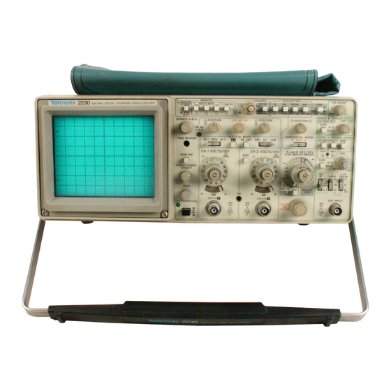
2230 Service SERVICING SAFETY SUMMARY FOR QUALIFIED SERVICE PERSONNEL ONLY Refer also to the preceding Operators Safety Summary. Oo Not Service Alone Disconnect power before removing protective panels, soldering, or replacing components. Do not perform internal service or adjustment of this pro... - Page 12 2230 Service 4998-01 The 2230 Digital Storage Oscilloscope.
-
Page 13: Section 1 General Information
GENERAL INFORMATION INTRODUCTION! The instrument is shipped with the following standard accessories: The TEKTRONIX 2230 Oscilloscope! is a combination nonstorage and digital storage dual-channel 100 MHz 1 Operators Manual bandwidth instrument. It is a rugged, lightweight oscillo 1 Users Reference Guide... - Page 14 General Information— 2230 Service Finite resolution affects any measurement using the horizontal axis. An averaged signal has a resolution of 100 points per division (ignoring expansion and compres discrete numbers. All digital storage stores amplitude sion). In addition, the averaged number is stored with up values as discrete numbers and associates those ampli...
- Page 15 General Information— 2230 Service Table 1-1 Electrical Characteristics Characteristics Performance Requirements VERTICAL DEFLECTION SYSTEM Deflection Factor Range 2 mV/div to 5 V/div in a 1-2-5 sequence. DC Accuracy (NON STORE) + 15°C to +3S°C Within ±2%. 0eC to +50°C Within ±3%.®...
- Page 16 General Information— 2230 Service Table 1-1 (cont) Characteristics Performance Requirements Aberrations (NON STORE and STORE in Default Modes) 2 mV/div to 50 mV/div +4%, -4 % , 4% p-p. 3% or less at + 25C C with cabinet installed. 0.1 V/div to 0.5 V/div +6%, -6 % , 6% p-p.
- Page 17 General Information— 2230 Service Table 1-1 (cont) Characteristics Performance Requirements REPETITIVE Store Mode SAMPLE and AVERAGE Single Trace 0.05 #is/div 100 MHz ( - 3 dB)b 100 MHz ( - 3 dB)6 0.1 MS/div 100 MHz ( - 3 dB)a' b 50 MHz (—3 dB)a...
- Page 18 General Information—2230 Service Table 1-1 (cont) Characteristics Performance Requirements NON STORE Common-Mode Rejection Ratio At least 10 to 1 at 50 MHz. (CMRR) Checked at 10 mV per division for common-mode signals of six divisions or less with the VOLTS/DIV Variable control adjusted for the best CMRR at 50 kHz.
- Page 19 General Information— 2230 Service Table 1-1 (cont) Characteristics Performance Requirements TRIGGERING SYSTEM A Trigger Sensitivity 10 MHz 60 MHz 100 MHz P-P AUTO and NORM 0.35 div 1.0 div 1.5 div Internal 40 mV 120 mV 150 mV External External trigger signal from a 50 n source driving a 50 Q coaxial cable terminated in 50 at the input connector.
- Page 20 General Information—2230 Service Table 1-1 (cont) Characteristics Performance Requirements HORIZONTAL DEFLECTION SYSTEM NON STORE Sweep Rates Calibrated Range A Sweep 0.5 sec per division to 0.05 per division in a 1-2-5 sequence of 22 steps.0 B Sweep 50 ms per division to 0.05 per division in a 1-2-5 sequence of 19 steps.0...
- Page 21 General Information— 2230 Service Table 1-1 (cont) Characteristics Performance Requirements STORE Mode Dynamic Range 10.24 divisions.8 STORE Mode Resolution Acquisition Record Length 1024 or 4096 data points.8 Single Waveform Acquisition Display 1024 data points (100 data points per division across the graticule area).8...
- Page 22 General Information— 2230 Service Table 1-1 (cont) Characteristics Performance Requirements DIGITAL STORAGE DISPLAY Vertical Resolution 10 bits (1 part in 1024).a Display waveforms are calibrated for 100 data points per division. Differential Accuracy Graticule indication of the voltage cursor difference is within 2% of the readout value, measured over the center six divisions.
- Page 23 General Information— 2230 Service Table 1-1 (cont) Characteristics Performance Requirements DIGITAL READOUT DISPLAY CURSOR Accuracy Voltage Difference Within ±3% of the AV readout value. Time Difference RECORD or ROLL/SCAN SAMPLE or AVERAGE ± 1 display interval.® PEAKDET or ACCPEAK +2 display intervals.
- Page 24 General Information—2230 Service Table 1-1 (cont) Characteristics Performance Requirements PROBE ADJUST Output Voltage on PRB ADJ Jack 0.5 V ±5%. Probe Adjust Signal Repetition Rate 1 kHz ±20%.a Z-AXIS Sensitivity (NON STORE Only) 5 V causes noticeable modulation. Positive-going input decreases intensity.
- Page 25 Table 1-2 Environmental Characteristics Characteristics Performance Requirements Environmental Requirements Instrument meets the requirements of Tektronix Standard 062- 2853-00, Class 5, except EMI. The instrument meets the following MIL-T-28800C requirements for Type III, Class 5 equipment, except where noted otherwise. Temperature Operating 0°C to +50®C (+ 3 2 ‘...
-
Page 26: Ch 2 Or Y, And Ext Input Connectors
General Information— 2230 Service Table 1-3 Physical Characteristics Characteristics Description See Figure 1-2 for dimensional drawing. Weight With Power Cord, Cover, 9.4 kg (20.7 lb). Probes, and Pouch With Power Cord Only 8.2 kg (18 lb). Domestic Shipping Weight 12.2 kg (26.9 lb). -
Page 27: Physical Dimensions Of The 2230 Oscilloscope
General Information— 2230 Service D i m e n s i o n s a r e i n c h e s [ m m ] 4735 4999-49 Figure 1-2. Physical dimensions of the 2230 Oscilloscope. 1-15... -
Page 28: Section 2 Operating Information
Available power-cord information is presented in Figure 2-2, and part numbers are listed in “Options and Accessories' (Section 7). Contact your Figure 2-1. Securing the detachable power-cord to the Tektronix representative or local Tektronix Field Office for instrument additional power-cord information. -
Page 29: Line Fuse
Operating Information— 2230 Service Plug Line Reference Usage Configuration Voltage Standards LINE FUSE North AN SI C73.11 American 120V N E M A 5-15-P 1 2 0 V / IEC 83 IS A C A U T IO N C A U T IO N... -
Page 30: Repackaging
Operating Information— 2230 Service normal operating mode. If the instrument fails one of the If the instrument is being shipped to a Tektronix power-up tests, the instrument attempts to indicate the Service Center for repair or calibration, attach a tag to the cause of the failure. -
Page 31: Controls, Connectors, And Indicators
Operating Information—2230 Service CONTROLS, CONNECTORS, AND INDICATORS ^ 8 ^ A INTENSITY Control— Adjusts the brightness of all The following descriptions are intended to familiarize NON STORE displayed waveforms. The control has the operator with the location and function of the no effect on the STORE mode displays or the crt instrument’s controls, connectors, and indicators. - Page 32 Operating Information— 2230 Service 4998-04 Figure 2-4. Power and display controls and power-on indicator.
-
Page 33: Vertical Controls And Connectors
Operating Information— 2230 Service Figure 2-5. Vertical controls and connectors. - Page 34 Operating information— 2230 Service CH 1 OR X and CH 2 OR Y Input Connectors— If properly coded probes (IX, 10X, or 100X, see Provide for application of signals to the inputs of the Table 2-1) are connected to a channel input connec...
-
Page 35: Horizontal
Operating Information—2230 Service In NON STORE X-Y mode, the CH 2 POSITION con acquiring and viewing both channel input signals at sweep rates of 0.5 ms per division and faster. trol vertically positions the display, the horizontal Channel 1 and Channel 2 STORE mode signals POSITION control positions the display horizontally, and the CH 1 POSITION control is not active. -
Page 36: Horizontal Controls
Operating Information— 2230 Service SEC/DIV Switch— Selects the calibrated A Sweep rates from 0.5 s to 0.05 MS/div in a 1-2-5 sequence of 22 steps for the A Sweep generator and sets the delay time scale factor for delayed- sweep operation. - Page 37 Operating Information—2230 Service SCAN Storage mode (for P-P AUTO TRIGGER enough that the acquisition can manually be mode with auto triggers disabled and 0.1 s/div to stopped when events of interest are observed. 5 s/div or EXT CLOCK) continuously updates the display serially as each data point is acquired.
- Page 38 Operating Information—2230 Service Variable SEC/DIV and 4K COMPRESS C o n tro l- AVERAGE Acquisition mode can be used for mul Controls the NON STORE sweep time per division tiple record averaging. A normalized algorithm is used for continuous display of the signal at full and compresses STORE mode waveform records.
-
Page 39: Trigger
Operating Information— 2230 Service The STORE mode display is the A Intensified TRIGGER trace only. The intensified zone on the A trace indicates the approximate delay position and Refer to Figure 2-7 for location of items 27 through 38. length of the B Delayed Sweep. The displayed... - Page 40 Operating Information— 2230 Service SGL SWP— Arms the A Trigger circuit for a single NORM— Permits triggering at all sweep rates (an sweep in NON STORE or a single acquisition in autotrigger is not generated in the absence of an STORE.
- Page 41 Operating Information— 2230 Service ) A EXT COUPLING Switch— Determines the method button is pressed in; the READY LE E D is turned on of coupling the signal applied to the EXT INPUT con when the filling is completed. The storage acquisition nector to the input of the A Trigger circuit.
-
Page 42: Storage Controls
Operating Information— 2230 Service control out of the CAL detent position. The STORAGE CONTROLS SEC/DIV readout is adjusted to reflect the correct time per division of the displayed waveform. The See Figure 2-8 for the location of items 38 through 42. - Page 43 Operating information—2230 Service CH 2; and Reference 3, CH 1 and CH 2. Cursors SAVE/CONTINUE Switch—Stops the current move to the acquisition waveform if they were on acquisition and display update in progress when a SAVE REF waveform that is turned off. The pressed in.
-
Page 44: Menu Selected Functions
Operating Information— 2230 Service Reference memory. The written waveform MENU SELECTED FUNCTIONS remains displayed on the crt. A control change or a delay of five seconds between This part describes the Menu selected functions that pressing SAVE button provide selection of parameters, settings, and features not selecting a memory location cancels the controlled by the front-panel switches. - Page 45 Operating Information— 2230 Service reordered data points between adjacent sample inter SPEED—Allows selection of plotter pen speed. vals. If the change in value does not exceed certain lim its, the values are interpreted as a continuous slope for A D V A N C E D FUNCTIONS drawing either vectors or dots.
-
Page 46: Rear Panel
Operating Information— 2230 Service In Peak Detect mode, the minimum and maximum lev els of the input signal within the time represented by 1/50 of a division unmagnified (1/25 of a division in CHOP or ALT) are digitized and stored in acquisition memory as a data pair. -
Page 47: Crt Readout
Operating Information— 2230 Service EXT CLK Input— Provides an input for EXT CLOCK signals (up to 1000 samples per second) to the storage acquisition circuitry in conjunction with the EXT CLK position of the A SEC/DIV switch. Samples are referenced by falling edges. -
Page 48: X-Y Plotter Interfacing
Operating Inform ation— 2230 Service Figure 2-11. X-Y Plotter interfacing. -
Page 49: Crt Readout Display
Operating Information— 2230 Service longer agree. In 4K COMPRESS, a c is displayed in front STORE Mode of the SEC/DIV readout. In STORE mode, many of the crt readout displays are associated with the parameters of stored waveforms. CURSOR READOUT. Displays the voltage difference (either AV 1 or AV 2) and the time difference between cur... -
Page 50: Operating Considerations
Operating Information— 2230 Service OPERATING CONSIDERATIONS This part contains basic operating information and tech GROUNDING niques that should be considered before attempting to make any measurements with the instrument. The most reliable signal measurements are made when the oscilloscope and the unit under test are connected by... -
Page 51: Input-Coupling Capacitor Precharging
Operating Information— 2230 Service components at or near the circuit’s resonant frequency. If AC input coupling is in use, the following procedure Oscillations (ringing) can then appear on the oscilloscope should be followed whenever the probe tip is connected to waveform display and distort the true signal waveshape. -
Page 52: Operator's Checks And Adjustments
Operating Information— 2230 Service OPERATOR’S CHECKS AND ADJUSTMENTS To verify the operation and basic accuracy of your Horizontal instrument before making measurements, perform the fol HORIZONTAL MODE lowing checks and adjustment procedures. If adjustments A SEC/DIV 0.5 ms are required beyond the scope of these operator's checks... -
Page 53: Trace Rotation Adjustment
Operating Information—2230 Service Check the waveform display for overshoot and TRACE ROTATION ADJUSTMENT rounding (see Figure 2-14); if necessary, use a small- bladed screwdriver to adjust the probe compensation for a NOTE square front corner on the waveform. Normally, the trace will be parallel to the center hor... -
Page 54: Horizontal Accuracy Check
Operating Information—2230 Service HORIZONTAL ACCURACY CHECK 11. Adjust the SEC/DIV switch setting for a display of at least one full period of the probe adjust signal (0.1 or A check of the horizontal timing can be made using the 0.2 ms per division), time measurement capability of the CURSOR measure... -
Page 55: Section 3 Theory Of Operation
GENERAL DESCRIPTION This section contains a functional description of the Introduction 2230 Digital Storage Oscilloscope. The discussion begins In the following overall functional description of the with a summary of instrument functions. Following the instrument, refer to the basic block diagram, Figure 3-1,... -
Page 56: Simplified Block Diagram
Theory of Operation— 2230 Service 4 9 9 9 -0 1 Figure 3-1. Simplified block diagram. - Page 57 Theory of Operation— 2230 Service trigger signal to the Trigger Amplifier when internal trigger Trigger signal, or a Line Trigger signal derived from the ing is selected. Other signal pickoffs provide vertical ac-power-source to develop trigger signals for the Sweep position information to the Position Signal Conditioning cir...
- Page 58 Theory of Operation—2230 Service transfers is provided by an external, crystal-controlled Switch position pickoffs supply the SEC/DIV switch setting oscillator that drives the Microprocessor clock generator. information to the Microprocessor for use in STORE mode horizontal timing. The A SEC/DIV switch setting is also The Microprocessor clock circuit further divides the input clock frequency to generate two lower clock frequencies.
- Page 59 Theory of Operation— 2230 Service actual clocking that occurs depends on the sampling mode signals generated by the Acquisition Clock Decoder (Min/Max, Sampling, or X-Y). The same waveform data is transfer the data from stage to stage in the digital acquisi...
- Page 60 Theory of Operation—2230 Service Digital-to-analog converters take the digital data bytes down by the Clock Generator to produce the various supplied from the Display Memory via the Display Con clocking rates. The Time Base Mode Register latches con troller and change them to the X- and Y-Axis analog trol data bits from the Microprocessor data bus to set the signals that drive the Horizontal and Vertical Vector Gen...
- Page 61 Operating Information—2230 Service ) A EXT COUPLING Switch— Determines the method button is pressed in; the READY LE E D is turned on of coupling the signal applied to the EXT INPUT con when the filling is completed. The storage acquisition nector to the input of the A Trigger circuit.
- Page 62 Operating Information— 2230 Service control out of the CAL detent position. The STORAGE CONTROLS SEC/DIV readout is adjusted to reflect the correct time per division of the displayed waveform. The See Figure 2-8 for the location of items 38 through 42.
- Page 63 Operating Information—2230 Service CH 2; and Reference 3, CH 1 and CH 2. Cursors Switch— Stops the current SAVE/CONTINUE move to the acquisition waveform if they were on acquisition and display update in progress when a SAVE REF waveform that is turned off. The pressed in.
- Page 64 Operating Information— 2230 Service Reference memory. The written waveform MENU SELECTED FUNCTIONS remains displayed on the crt. A control change or a delay of five seconds between This part describes the Menu selected functions that pressing SAVE button provide selection of parameters, settings, and features not selecting a memory location cancels the controlled by the front-panel switches.
- Page 65 Operating Information— 2230 Service reordered data points between adjacent sample inter SPEED—Allows selection of plotter pen speed. vals. If the change in value does not exceed certain lim its, the values are interpreted as a continuous slope for ADVANCED FUNCTIONS drawing either vectors or dots.
- Page 66 Operating Information— 2230 Service In Peak Detect mode, the minimum and maximum lev els of the input signal within the time represented by 1/50 of a division unmagnified (1/25 of a division in CHOP or ALT) are digitized and stored in acquisition memory as a data pair.
- Page 67 Operating Information— 2230 Service EXT CLK Input— Provides an input for EXT CLOCK signals (up to 1000 samples per second) to the storage acquisition circuitry in conjunction with the EXT CLK position of the A SEC/DIV switch. Samples are referenced by falling edges.
- Page 68 Operating Information— 2230 Service Figure 2-11. X-Y Plotter interfacing.
- Page 69 Operating Information— 2230 Service longer agree. In 4K COMPRESS, a c is displayed in front STORE M ode of the SEC/DIV readout. In STORE mode, many of the crt readout displays are associated with the parameters of stored waveforms. CURSOR READOUT. Displays the voltage difference (either AV 1 or AV 2) and the time difference between cur...
- Page 70 Operating Information— 2230 Service OPERATING CONSIDERATIONS This part contains basic operating information and tech GROUNDING niques that should be considered before attempting to make any measurements with the instrument. The most reliable signal measurements are made when the oscilloscope and the unit under test are connected by...
- Page 71 Operating Information— 2230 Service components at or near the circuit’s resonant frequency. If AC input coupling is in use, the following procedure Oscillations (ringing) can then appear on the oscilloscope should be followed whenever the probe tip is connected to waveform display and distort the true signal waveshape.
- Page 72 Operating Information— 2230 Service OPERATOR’S CHECKS AND ADJUSTMENTS To verify the operation and basic accuracy of your H o riz o n ta l instrument before making measurements, perform the fol HORIZONTAL MODE lowing checks and adjustment procedures. If adjustments A SEC/DIV 0.5 ms...
- Page 73 Operating Information—2230 Service Check the waveform display for overshoot and TRACE ROTATION ADJUSTMENT rounding (see Figure 2-14); if necessary, use a small- bladed screwdriver to adjust the probe compensation for a NOTE square front corner on the waveform. Normally, the trace will be parallel to the center hor...
- Page 74 Operating Information— 2230 Service HORIZONTAL ACCURACY CHECK 11. Adjust the SEC/DIV switch setting for a display of at least one full period of the probe adjust signal (0.1 or A check of the horizontal timing can be made using the 0.2 ms per division),...
- Page 75 GENERAL DESCRIPTION This section contains a functional description of the Introduction 2230 Digital Storage Oscilloscope. The discussion begins In the following overall functional description of the with a summary of instrument functions. Following the instrument, refer to the basic block diagram, Figure 3-1,...
- Page 76 Theory of Operation— 2230 Service 4 9 9 9 -0 1 Figure 3-1. Simplified block diagram.
- Page 77 Theory of Operation— 2230 Service trigger signal to the Trigger Amplifier when internal trigger Trigger signal, or a Line Trigger signal derived from the ing is selected. Other signal pickoffs provide vertical ac-power-source to develop trigger signals for the Sweep position information to the Position Signal Conditioning cir...
- Page 78 Theory of Operation—2230 Service transfers is provided by an external, crystal-controlled Switch position pickoffs supply the SEC/DIV switch setting oscillator that drives the Microprocessor clock generator. information to the Microprocessor for use in STORE mode horizontal timing. The A SEC/DIV switch setting is also The Microprocessor clock circuit further divides the input clock frequency to generate two lower clock frequencies.
- Page 79 Theory of Operation— 2230 Service actual clocking that occurs depends on the sampling mode signals generated by the Acquisition Clock Decoder (Min/Max, Sampling, or X-Y). The same waveform data is transfer the data from stage to stage in the digital acquisi...
- Page 80 Theory of Operation— 2230 Service Digital-to-analog converters take the digital data bytes down by the Clock Generator to produce the various supplied from the Display Memory via the Display Con clocking rates. The Time Base Mode Register latches con troller and change them to the X- and Y-Axis analog trol data bits from the Microprocessor data bus to set the signals that drive the Horizontal and Vertical Vector Gen...
-
Page 81: Detailed Circuit Description
DETAILED CIRCUIT DESCRIPTION The detailed circuit description of the 2230 first The Attenuator circuit and switches (see Figure 3-2) describes the analog operating portion of the oscilloscope provide control of the input coupling, the vertical deflection followed by the digital portion. -
Page 82: Block Diagram Of The Channel 1 Attenuator Circuit
Theory of Operation— 2230 Service 4 9 9 9 - 0 2 Figure 3-2. Block diagram of the Channel 1 Attenuator circuit... - Page 83 Theory of Operation— 2230 Service ac coupled, the input signal must go through dc-blocking switch (S10) determines whether the Paraphase Amplifier capacitor C2. The blocking capacitor stops the dc com receives a signal attenuated by a factor of 1 (no attenua...
-
Page 84: Vertical Preamplifiers
Theory of Operation— 2230 Service Vertical Position conditioning circuit where dc offset adjust reversed, reversing the polarity of the output signal to pro ments provide tracking corrections between the vertical duce an inverted Channel 2 trace and Channel 2 storage acquisition signal. -
Page 85: Store-Non Store Vertical Switching
Theory of Operation— 2230 Service POSITION CH 1 SIGNAL POSITION TO CH 1 CONDITIONING STORAGE POSITION POSITION AMPL R112 0114 Q115 POS + POS - COMMON CH 1 CH 1- CH 1- BASE SIGNAL AMPL FROM CH 1+ CH 1+... -
Page 86: Vertical Output Amplifier
Theory of Operation— 2230 Service ADD DISPLAY. In the ADD position of S545, both the The nonstore output transistors are biased off by set Set and Reset inputs_of U540A are held LO by CR534 and ting pins 9 and 12 of U7201 LO. The forward bias is CR537. -
Page 87: Triggering
Theory of Operation— 2230 Service Q202 and Q203 through R202 and R203 to return the out trace with respect to the Nonstore A trace in BOTH Hor put of the Delay Line Driver to an average dc voltage of izontal mode. In the B Sweep interval, the SEP signal from zero. - Page 88 Theory of Operation— 2230 Service HORIZ OUTPUT B TRIGGER LEVEEL COMPARATOR A TRIGGER LEVEL COMPARATOR 49S9-04 Figure 3-4. Block diagram ot Trigger Amplifiers and Switching, 3-14...
- Page 89 Theory of Operation— 2230 Service One transistor in each side of the output differential CHANNEL 1. For triggering from Channel 1, the A&B amplifier pairs of U310 has its base bias set to a fixed INT switch is set to CH 1. The XY line connected to S555 level by the divider network formed by R321 and R322.
- Page 90 Theory of Operation— 2230 Service The CHOP VERTICAL MODE position grounds the In the P-P AUTO and TV FIELD Trigger modes, Q413 base of Q541 and puts a LO on an input, of both U555B is biased off, and CR414 and CR415 are reverse biased.
-
Page 91: A Sweep Generator And Logic
Theory of Operation— 2230 Service switch to the voltage set by the A TRIGGER LEVEL con A SWEEP GENERATOR AND LOGIC trol and produces an output trigger signal at the correct level. Rising or falling slope triggering is selected by the The A Sweep Generator and Logic circuitry, shown on front-panel A TRIGGER SLOPE switch. - Page 92 Theory of Operation— 2230 Service HORIZONTAL B SHEEP GENERATOR Z-AXIS 4 9 9 9 - 0 5 Figure 3-5. A Sweep Generator and Logic circuitry. 3-18...
- Page 93 Theory of Operation— 2230 Service current through the timing capacitors, which results in a U502 is also used in the Auto Baseline circuit as described in the "P-P AUTO and TV FIELD” part of the discussion linearly increasing voltage ramp as they charge. The ramp that follows.
-
Page 94: B Timing And Alternateb Sweep
Theory of Operation— 2230 Service Storage signal acquisition. The Store signal forward biases If trigger signals are being received, U502 remains set. As CR7140 to override the XY signal, and the A Sweep Logic long as U502 is set, the output of U532D is HI, causing the output of U532C to be LO. - Page 95 Theory of Operation— 2230 Service control R602 is rotated fully clockwise. In this position of In the RUNS AFTER DELAY mode, the Run After R602, transistor Q637 is biased off, and a LO is present at Delay circuit holds the D input of flip-flop U670A LO via its collector.
- Page 96 Theory of Operation— 2230 Service Alternate Display Switching Logic SWP SEP. Whenever the B Sweep is selected to drive the Horizontal Amplifier, the Q output of U670B is HI. This The Alternate Display Switching Logic circuitry controls HI goes to U665C pin 10 through Q683 and Q687, and...
-
Page 97: Horizontal
Theory of Operation— 2230 Service and off. A second set of contacts on S721 informs the HORIZONTAL Microprocessor whether X I0 Magnification is off or on. The SEC/DIV readout is automatically set to the correct The Horizontal Amplifier circuit, shown on Diagram 7,... -
Page 98: Horizontal Amplifier Block Diagram
Theory of Operation— 2230 Service 4 9 9 9 - 0 6 Figure 3-6. Horizontal Amplifier block diagram. 3-24... -
Page 99: Microprocessor And Store-Panel Controls
Theory of Operation— 2230 Service Transistors Q770, Q775, and Q779, as one-half of the MICROPROCESSOR AND complementary differential circuit, form cascode- STORE-PANEL CONTROLS feedback amplifier for driving the right crt horizontal deflection plate. Amplifier gain is set by R775, with C775 The Microprocessor, shown on Diagram 14, directs the providing high-frequency compensation. -
Page 100: Status Adc And Bus Interface
Theory of Operation—2230 Service automatically fetches the first command from the reset in addition, when one of the Communication Options is vector (address 0FFFF0), and begins program execution. installed, the RDY1 input (U9104 pin 4) is used to syn Other interrupts: to the Microprocessor cause vectoring to chronize the operation of the Microprocessor with the addresses that start the interrupt handling routines. - Page 101 Theory of Operation— 2230 Service Table 3-1 Memory Space Allocation Block Designation Block Address (Hex) Space Allocation Purpose RAM SEG 00000-3FFFF Four images of Memory Segment 0 RAM Primary 00000-07FFF 8-bit display RAM—waveforms, interrupt vectors, miscellaneous. 08000-0FFFF 4 bits of display RAM for waveform attributes (LSB).
-
Page 102: Storage Acquisition
Theory of Operation—2230 Service Table 3-1 (cont) Block Address (Hex) Space Allocation Purpose Block Designation 98000-BFFFF Option Duplicate Image C0000-FFFFF Two images of Memory Segment 3 ROM SEGMENT C0000-DFFFF ROM Duplicate Image E0000-E7FFF System ROM 0— Low half of U9109. - Page 103 Theory of Operation— 2230 Service Common-base transistors, Q2101 and Q2102 form a The sample-bridge strobe pulse is developed from the differential amplifier that presents a low-impedance load ADC clock signals by U2203B, U2203A, and the RC circuit for the Channel Switch. Offset is adjusted (using poten...
-
Page 104: Acquisition Memory
Theory of Operation—2230 Service a high-speed ECL device having ECL compatible open- M IN/MAX R egisters emitter outputs. Pull-down resistors to the —5 V supply Data is latched into the MIN/MAX Registers in four are in resistor pack R2295. The ECL output levels are different ways depending on the acquisition mode. - Page 105 Theory of Operation— 2230 Service Figure 3-7. Sampling mode acquisition timing at 0.05 S per division (ADCLK=CONV—20 MHz). 3-31...
- Page 106 Theory of Operation— 2230 Service function of the SEC/DIV switch setting). As the SAVECLK mode, flip-flop U3306A is held in the Set state (reset is period increases with slower SEC/DIV switch settings, the also LO, so both outputs of the flip flop are HI). Each ris...
- Page 107 Theory of Operation— 2230 Service CONV U4102B-10 ADCLK U4102A-6 SAVECLK U4125B-9 EVENCLK U3101B-9 BUFFERCLK U3103A-5 MINCLK (CHI) U3309-7 MAXCLK (CH2) U3309-9 IN IT STROBE U3309-14 Figure 3-8. MIN/MAX Acquisition timing at 20 ps per division. 3 -3 3...
- Page 108 Theory of Operation— 2230 Service Another section of the circuitry is used in conjunction When that LO is clocked through U3307B, NAND-gate with the Min-Max Sampling mode to determine whether U3313B goes LO, passing and inverting the DATAEN ena bling signal. That makes SWAP LO, and the swapping the last sample clocked into the MIN/MAX Registers was a NEWMIN or a NEWMAX.
- Page 109 Theory of Operation— 2230 Service CHANNEL SELECT. When only Channel 1 or Channel 2 Before the start of an acquisition, U3105A pin 1 is held LO by ACQENA. The LO keeps U3105A reset, putting a is selected, the Microprocessor controls the choice via the LO on U3105A pin 5 and 1)3104C pin 9.
- Page 110 Theory of Operation— 2230 Service pin 1 of U3112A, and NAND-gate U3112 is disabled from memory is enabled for reading stored data, pin 4 is LO passing the selected clock signal. U3112A puts a HI on (RD). The ASQSEL signal is inverted by U3416B and pin 13 of U3112D, enabling U3112D to pass the divided applied to pin 5 of the multiplexer.
-
Page 111: Acquisition Memory Timing
Theory of Operation— 2230 Service - Figure 3-9. Acquisition Memory timing. 3-37... -
Page 112: Digital Time Base
Theory of Operation— 2230 Service Acquisition Memory Address Registers access by the Microprocessor. The memory address to be written to or read from is controlled by the Address These registers pass the address count onto the Counter. Microprocessor data bus when enabled. Registers U3427 and U3428 are enabled during different I/O periods. - Page 113 Theory of Operation— 2230 Service 40MHz CLOCK Y 4 1 0 0 -8 ADCLK 20MHZ U 4 102A -6 CONV CLK .0 5 /is 20MHZ 1 0 /is /D IV U 4102B -10 WRITECLK 10MHZ U 4104A -6 RNGB U 4 1 0 3 -2 •...
- Page 114 Theory of Operation— 2230 Service reset when the ACQENA signal is LO. ACQENA is clocked data into the register. The data bits loaded determine the HI by the CONV clock going HI (one-half CONV clock number of times the CONV 10 MHz clock is divided to pro...
- Page 115 Theory of Operation— 2230 Service Table 3-3 Time Base Clock Frequencies CONV SEC/DIV SAVECLK RECCLK SAVECLK RANGE SOURCE 0.05 /is 20 MHz 10 MHz 20 MHz CONV/2 20 MHz 0.1 M S 10 MHz 20 MHz CONV/2 20 MHz 10 MHz...
- Page 116 Theory of Operation— 2230 Service Table 3-4 Time Base Divider Preload Bits Divider DD Bits SAVE CLOCK DIVIDER SEC/DIV Divide 7 6 5 4 3 2 1 0 Setting Frequency Output Ratio 1 1 1 1 1 1 0 0 2.5 MHz...
- Page 117 Theory of Operation— 2230 Service Table 3-5 Trigger Logic Multiplexer Switching CALTIMER A/BTRIG TEST TRIGGER MODE SELECTED SIGNAL A TRIG A GATE B TRIG B GATE MIN COUNT CONV MAX COUNT CONV must know the information to place the data samples into clock, so depending on the state of the Q output when the the correct locations in Display Memory.
-
Page 118: Digital Display
Theory of Operation— 2230 Service Resistor R4213 and C4202 adjust the counter’s gain A d d re s s D e c o d e r and offset. Nominal counts are 300 for maximum and 100 To access a byte in RAM, a row address followed by a for minimum. -
Page 119: Vector Generator
Theory of Operation— 2230 Service These circuits also have a “ dot” mode available so that When reading data out of the RAM, the Display Con the integrator outputs are stepped (dots) rather than con troller has direct access to the memory address bus (RA). - Page 120 Theory of Operation— 2230 Service U6305 pin 14. That signal in turn is controlled by the P lo t D rive PLT-EN signal (U6301B pin 9) that switches section B of When plot mode is on, the display controller activates multiplexer U6301.
-
Page 121: Power Input, Preregulator And Inverter
Theory of Operation— 2230 Service their respective chokes. Feedback is applied to the com POWER INPUT, PREREGULATOR parators causing duty cycle and frequency modulation, AND INVERTER which adjusts output power accordingly. The Power Supply (see Diagram 8 and Diagram 9) changes the ac power-line voltage into the voltages +5 VOLT POWER SUPPLY. - Page 122 Theory of Operation— 2230 Service oscillator that operates at a frequency set by R919 and VR935 conducts, causing Q935 to also conduct. The Preregulator output current is then shunted through Q935, C919 (approximately 60 kHz). A sawtooth voltage pro duced at pin 5 of U930 is compared internally with the out...
-
Page 123: Power Supply Secondaries, Z-Axis And Crt
Theory of Operation— 2230 Service gain for changing the input current to a proportional output base drive of Q944 and, thereby, controls the voltage on voltage. Emitter-follower Q835 is dc coupled to Q840, and C944. This voltage biases Q946 and Q947 to a level that for low-speed signals, Q845 acts as a current source. -
Page 124: Simplified Diagram Of The Dc Restorer Circuitry
Theory of Operation— 2230 Service triggered or not), and the INTENSITY controls and the Z- For a Nonstore X-Y display CR818, CR817, and CR816 are reverse biased. The XY signal is LO to reverse Axis drive signals have no control over the crt intensity. -
Page 125: X-Y Plotter
Theory of Operation— 2230 Service CR851, CR853, and R854 to the Z-Axis output level. Neon lamp DS870 protects against excessive voltage Thus, the ac-drive voltage is clamped at two levels to pro between the crt heater and crt cathode by conducting if duce a square-wave signal with a positive dc-offset level. - Page 126 Theory of Operation— 2230 Service accomplished by providing the Pen-Down signal to the Signal Ground operational amplifier about 1 s prior to the signals- being The AUXILIARY CONNECTOR SIG GND connection provided to X & Y plot output circuitry. This allows the...
-
Page 127: Section 4 Performance Check Procedure
Section 4— 2230 Service PERFORMANCE CHECK PROCEDURE INTRODUCTION PURPOSE "Adjustment Procedure” in Section 5. Test equipment specifications described in Table 4-1 are the minimum The “ Performance Check Procedure” is used to verify necessary to provide accurate results. Therefore, equip... - Page 128 Performance Check Procedure—2230 Service Table 4-1 Test Equipment Required Minimum Example of Suitable Item and Specification Test Equipment Description Purpose Standard-amplitude signal levels: Signal source for gain TEKTRONIX PG 506 1. Calibration Generator 5 mV to 50 V. Accuracy: ± 0.3%.
-
Page 129: Index To Performance Check Steps
Performance Check Procedure— 2230 Service Table 4-1 (cont) Item and Minimum Example of Suitable Description Specification Purpose Test Equipment Signal termination. 13. Termination Impedance: 600 9. Connectors: BNC. Tektronix Part Number 011-0092-00. Vertical compensation 14. 10X Attenuator Ratio: 10X. Impedance: 50 9. Con... -
Page 130: Vertical
Performance Check Procedure— 2230 Service VERTICAL Equipment Required (see Table 4-1): Calibration Generator (Item 1) Dual-Input Coupler (Item 9) Leveled Sine-Wave Generator (Item 2) 50 0 BNC Termination (Item 12) 50 0 BNC Cable (Item 8) 10X Attenuator (Item 14) - Page 131 Performance Check Procedure—2230 Service Move the cable from the CH 1 OR X input connector Move the cable from the CH 2 OR Y input connector to the CH 2 OR Y input connector. Set the VERTICAL to the CH 1 OR X input connector, set the VERTICAL MODE switch to CH 2.
- Page 132 Performance Check Procedure— 2230 Service e. Set: 4. Check Position Range VERTICAL MODE CH 2 a. Set: STORE/NON STORE NON STORE 50 mV VOLTS/DIV (both) AC-GND-DC (both) f. Repeat parts b through d for Channel 2 trace. STORE/NON STORE NON STORE (button out) g.
- Page 133 Performance Check Procedure— 2230 Service g. Repeat part f for each of the following VOLTS/DIV c. Set the generator to produce a 1 MHz, 5-division display. switch settings: 5 mV through 0.5 V. Adjust the generator output and attach or remove the 10X attenuator as neces...
- Page 134 Performance Check Procedure— 2230 Service e. Repeat parts c and d for all indicated CH 2 10. Check Single Sweep Sample Acquisition VOLTS/DIV switch settings, up to the output-voltage a. Set: upper limit of the sine-wave generator being used. CH 1...
- Page 135 Performance Check Procedure— 2230 Service p. Disconnect the test equipment from the instrument. 12. Check Common-Mode Rejection Ratio a. Set: BW LIMIT Off (button out) CH 2 VOLTS/DIV 10 mV 13. Check Non Store and Store Channel Isolation INVERT On (button in) a.
- Page 136 Performance Check Procedure—2230 Service k. Use the Channel 2 POSITION control to center the I. Set: display. VERTICAL MODE CH 1 CH 1 VOLTS/DIV 50 mV CH 2 VOLTS/DIV 0.1 V I. Set CH 2 VOLTS/DIV switch to 50 mV for a 10- Channel 1 AC-GND-DC division display.
- Page 137 Performance Check Procedure— 2230 Service j. Set the generator to produce a 0.1 s period, 2 ms n. Repeat parts c and d. pulse duration, 5-division display. o. Disconnect the test equipment from the instrument. k. Repeat parts c through h.
-
Page 138: Horizontal
Performance Check Procedure— 2230 Service HORIZONTAL Equipment Required (see Table 4-1): Calibration Generator (Item 1) BNC Cable (Item 8) Leveled Sine-Wave Generator (Item 2) 50 fl BNC Termination (Item 12) Time-Mark Generator (Item 3) INITIAL CONTROL SETTINGS PROCEDURE STEPS Vertical 1. - Page 139 Performance Check Procedure— 2230 Service Table 4-5 Set: Settings for Timing Accuracy Checks HORIZONTAL MODE A SEC/DIV SEC/DIV 0.05 /is Time-Mark Generator Setting B SEC/DIV X I0 Magnifier Off (knob in) Switch Setting X10 Magnified Normal (X I) Repeat parts b through k for the B Sweep. Keep 0.05 fts...
- Page 140 Performance Check Procedure—2230 Service d. Set: j. Press in the C1/C2 button to activate the second cursor. Channel 1 AC-GND-DC SEC/DIV Variable CAL detent HORIZONTAL MODE BOTH k. Set the second cursor on the trailing edge of the 10th time marker at the same voltage level as on the 2nd time marker.
- Page 141 Performance Check Procedure— 2230 Service Rotate the B DELAY TIME POSITION control fully 6. Check Position Range clockwise until the top of the 10th time marker on the B a. Set: Sweep is aligned with the same selected reference vertical line as in part j.
- Page 142 Performance Check Procedure— 2230 Service e. Set the X I0 Magnifier knob to On (knob out). 10. Check X Gain a. Set: f. CHECK—The time markers are 1 division apart. On (button in) CH 1 VOLTS/DIV 10 mV Horizontal POSITION Midrange 8.
-
Page 143: Trigger
Performance Check Procedure— 2230 Service TRIGGER Equipment Required (see Table 4-1): Leveled Sine-Wave Generator (Item 2) Dual-Input Coupler (Item 9) Low Frequency Generator (Item 4) BNC Termination (Item 12) 50 0 BNC Cable (Item 8) 600 n BNC Termination (Item 13) - Page 144 Performance Check Procedure— 2230 Service Set the generator to produce a 100 MHz, 1.5- Table 4-7 division display. Switch Combinations for A Triggering Checks A TRIGGER SLOPE A TRIGGER Mode Repeat parts d through f. NORM Set: NORM P-P AUTO...
- Page 145 Performance Check Procedure— 2230 Service Set: 4. Check External Trigger Ranges a. Set: VERTICAL MODE CH 2 A&B INT CH 2 CH 1 VOLTS/DIV 0.5 V A SEC/DIV X I0 Magnifier Off (knob in) Move the cable from the CH 1 OR X input connector A TRIGGER SLOPE to the CH 2 OR Y input connector.
- Page 146 Performance Check Procedure— 2230 Service e. CHECK— READY LED goes out and a single sweep CHECK— The A TRIG POS default number is 3584 occurs. and the trigger point (T) appears near the 9th vertical grat icule line below the Menu.
-
Page 147: External Z-Axis, Probe Adjust, External Clock, And X-Y Plotter
Performance Check Procedure— 2230 Service EXTERNAL Z-AXIS, PROBE ADJUST, EXTERNAL CLOCK, AND X-Y PLOTTER Equipment Required (see Table 4-1): BNC T-Connector (Item 11) Leveled Sine-Wave Generator (Item 2) Pulse Generator (Item 5) 50 Q BNC Termination (Item 12) Digital Voltmeter (Item 7) - Page 148 Performance Check Procedure— 2230 Service 3. Check External Clock b. Set the digital voltmeter to the 20 V scale. a. Set: C. Set the WAVEFORM REFERENCE/MENU SELECT CH 1 VOLTS/DIV switch to MENU SELECT (button out). A SEC/DIV 1 ms d.
-
Page 149: Section 5 Adjustment Procedure
Section 5— 2230 Service ADJUSTMENT PROCEDURE INTRODUCTION PURPOSE that recommended, utilize the "Minimum Specification” column to determine whether available test equipment will suffice. The "Adjustment Procedure" is a set of logically sequenced instructions intended to return the instrument to conformance with the Performance Requirement state... - Page 150 Adjustment Procedure— 2230 Service allow access to the internal adjustments. See power-supply adjustment. Altering this adjustment may latched to the "Storage Circuit Board in Servicing Position” pro necessitate a complete readjustment of the instrument, cedure in the "Removal and Replacement Instructions”...
-
Page 151: Index To Adjustment Procedure Steps
Adjustment Procedure— 2230 Service Horizontal Page INDEX TO ADJUSTMENT 1. Adjust Horizontal Amplifier Gain......5-19 PROCEDURE STEPS 2. Adjust X I0 Horizontal Amplifier Gain....5-20 3. Adjust Magnifier Registration....... 5-20 Power Supply and CRT Display Page 4. Check Sweep Length........... 5-20 1. -
Page 152: Power Supply And Crt Display
Adjustment Procedure— 2230 Service POWER SUPPLY AND CRT DISPLAY Equipm ent Required (See Table 4-1): . — Leveled Sine-Wave Generator (Item 2) 50 ft BNC Cable (Item 8) Time-Mark Generator (Item 3) 50 ft BNC Termination (Item 12) Digital Voltmeter (Item 7) - Page 153 Adjustment Procedure— 2230 Service Adjust Trace Alignment Table 5-2 Position the trace to the center horizontal graticule Power Supply Limits line. Reading Test Power (Volts) Supply Point ADJUST—The front-panel TRACE ROTATION con trol for optimum alignment of the trace with the center hor...
-
Page 154: Vertical
Adjustment Procedure— 2230 Service VERTICAL Equipment Required (See Table 4-1): Calibration Generator (Item 1) 10X Attenuator (Item 14) Leveled Sine-Wave Generator (Item 2) BNC Male-to-Miniature-Probe Tip (Item 16) 50 f) BNC Cable (Item 8) Low-Capacitance Alignment Tool (Item 18) Dual-Input Coupler (Item 9) Screwdriver (Item 19) 50 £... - Page 155 Adjustment Procedure— 2230 Service f. Set the VERTICAL MODE switch to CH 2. Adjust Channel 2 Invert Balance (R75) a. Set the VERTICAL MODE switch to CH 2. g. Repeats parts a through e for Channel 2, adjusting Step Attn Bal (R60) in part c.
- Page 156 Adjustment Procedure— 2230 Service ADJUST— MF/LF Comp (C3) and MF/LF Gain Bal CHECK—That no trace shift occurs when switching (R47) for the best front corner and flat top. between the 5 mV and 2 mV positions of the CH 1 VOLTS/DIV switch.
- Page 157 Adjustment Procedure— 2230 Service 10. Adjust/Check Acquisition Vertical Position c. Move the cable from the CH 1 OR X input connector Registration (R2138) and Horizontal Position to the CH 2 OR Y input connector. Set the VERTICAL Registration (R6430 SN-B022102 & Above) MODE switch to CH 2.
- Page 158 A d ju s tm e n t P ro c e d u re — 2 2 3 0 S e rv ic e Position the trace 0.5 division below the top horizon g. ADJUST—Ch 1 Acq Gain (R2118) for an exact 5- graticule line using the Channel 1 POSITION control.
- Page 159 Adjustment Procedure— 2230 Service 13. Adjust Store Y Offset and Gain (R9224 and f. ADJUST—Ch 1 Acq Pos Offset (R7325) for R9222) minimum separation of the Channel 1 baseline and the short trace at the top and bottom of the screen.
- Page 160 Adjustment Procedure— 2230 Service g. ADJUST—The 10X Attn (Cl 2) for best front corner. h. Set the SAVE/CONTINUE switch to SAVE (button in). Table 5-5 i. Set the CH 2 VOLTS/DIV switch to 1 V. Attenuator Compensation Adjustments j. CHECK—The display is compressed to 0.5 division...
- Page 161 Adjustment Procedure— 2230 Service u. Repeat parts b through s for Channel 2 attenuators. 19. Adjust High-Frequency Compensation (C237, R240 and R241) and Channel 2 High-Frequency Compensation v. Disconnect the test equipment from the instrument. (C180) a. Set: VERTICAL MODE CH 1 17.
- Page 162 Adjustment Procedure— 2230 Service m. Set the generator to produce a 5-division display. c. Use the Menu controls to call up SELECT MODE Table on the screen and select AVERAGE with the SELECT C1/C2 button. Reset WAVEFORM n. Set the top of the display to the center horizontal REFERENCE/MENU SELECT switch to WAVEFORM graticule line using the Channel 2 POSITION control.
- Page 163 Adjustment Procedure—2230 Service 22. Check Store Mode Cross Talk 23. Check Store Pulse Width Amplitude a. Set: a. Set: BOTH and CHOP AC-GND-DC (both) VERTICAL MODE Channel 1 AC-GND-DC VERTICAL MODE Channel 2 AC-GND-DC SEC/DIV 1 ms VOLTS/DIV (both) STORE/NON STORE 0.1 V...
- Page 164 Adjustment Procedure—2230 Service m. Set the generator to produce a 1 ms period, 20 26. Check Bandwidth duration, 5-division display. a gel; BW LIMIT Off (button out) n. Repeat parts c and d. VOLTS/DIV (both) 2 mV o. Disconnect the test equipment from the instrument.
- Page 165 A djustm ent P rocedure— 2 2 3 0 S e rv ic e d. Set the generator to produce a 100 MHz display. 29. Check Non Store and Store Channel Isolation Set: e. Set: VOLTS/DIV (both) 0.1 V VOLTS/DIV Variable (both) CAL detent STORE/NON STORE STORE (button in)
- Page 166 Adjustment Procedure— 2230 Service . CHECK— Display amplitude is 0.1 division or less. m. Set the generator to produce a 50 MHz, 6-division display. m. Disconnect the test equipment from the instrument. n. Set the VERTICAL MODE switch to BOTH.
-
Page 167: Horizontal
Adjustment Procedure— 2230 Service HORIZONTAL Equipm ent Required (See Table 4-1): Calibration Generator (Item 1) 50 0 Cable (Item 8) Leveled Sine-Wave Generator (Item 2) 50 0 BNC Termination (Item 12) Time-Mark Generator (Item 3) Low-Capacitance Alignment Tool (Item 18) - Page 168 Adjustment Procedure— 2230 Service d. Set the HORIZONTAL MODE switch to B. b. Position the start of the sweep at the 1st vertical graticule line using the Horizontal POSITION control. e. ADJUST— B Sweep Gain (R730) for 1 time marker per division.
- Page 169 Adjustment Procedure— 2230 Service c. Adjust the A/B SWP SEP control to separate the A b. Select 0.5 ms time markers from the time-mark and B Sweeps. generator. d. Position the start of the trace exactly on the 1st c. CHECK—Time markers are 1 division or less apart.
- Page 170 Adjustment Procedure— 2230 Service c. ADJUST—A High Speed Timing (C703) for 1 time c. Adjust the A TRIGGER LEVEL control for a stable, marker per division over the center 8 divisions. triggered display. d. Use the Horizontal POSITION control to align the d.
- Page 171 Adjustment Procedure— 2230 Service Use the Horizontal POSITION control to align the Table 5-7 start of the A Sweep with the 1 st vertical graticule line. Settings for Timing Accuracy Checks Set the B DELAY TIME POSITION control fully Time-Mark Generator Setting SEC/DIV counterclockwise.
- Page 172 Adjustment Procedure—2230 Service Table 5-8 15. Adjust Store X Offset and Gain (R9214 and R9212) Settings for Delay Time Differential Checks ADJUST—Store X Offset (R9214) so that the left trace of the outside box is exactly aligned with the 1st...
- Page 173 Adjustment Procedure— 2230 Service CHECK—Graticule indication of cursor difference at NOTE the 10th vertical graticule line is within 0.16 division. Pulses with fast rise and fall times have only a few sample points, and it may not be possible to place the cursors at exactly the same voltage levels.
- Page 174 Adjustment Procedure— 2230 Service b. Connect the leveled sine-wave generator output via b. Connect the standard-amplitude signal from the a 50 f] cable and a 50 £ ) termination to the CH 1 OR X Calibration Generator via a 50 Q cable to the CH 1 OR X input connector.
-
Page 175: Trigger
Adjustment Procedure— 2230 Service TRIGGER Equipment Required (See Table 4-1): Leveled Sine-Wave Generator (Item 2) BNC T-Connector (Item 11) Low-Frequency Generator (Item 4) 50 S i BNC Termination (Item 12) 50 0 BNC Cable (Item 8) 600 fl BNC Termination (Item 13) - Page 176 Adjustment Procedure— 2230 Service f. Set the A&B INT switch to CH 2. d. ADJUST—(+) P-P Auto Level (R434) so that the vertical display just solidly triggers on the positive peak of the signal. g. Repeat parts c through f until there is 1 mV or less difference in the voltmeter readings between the CH 1 and CH 2 positions of the A&B INT switch.
- Page 177 Adjustment Procedure— 2230 Service Set the HORIZONTAL MODE switch to B. s. Repeat parts e through g. CHECK— Stable display can be obtained by adjust- t. Set: ing the B TRIGGER LEVEL control in a position other than the B RUNS AFTER DLY position for both the OUT and...
- Page 178 Adjustment Procedure— 2230 Service 7. Check External Trigger Ranges h. Move the cable from the CH 1 OR X input connector to the CH 2 OR Y input connector. a. Set: 0.5 V CH 1 VOLTS/DIV i. Repeat part f.
- Page 179 Adjustment Procedure— 2230 Service Set the PRETRIG/POST TRIG switch to PRETRIG e. CHECK— READY LED goes out and a single sweep (button in). occurs. f. Press in the SGL SWP button several times. CHECK—The A TRIG POS default number is 3584 and the trigger point (T) appears near the 9th vertical grat...
-
Page 180: External Z-Axis, Probe Adjust, External Clock, And X-Y Plotter
Adjustment Procedure— 2230 Service EXTERNAL Z-AXIS, PROBE ADJUST, EXTERNAL CLOCK, AND X-Y PLOTTER Equipment Required (se e T able 4-1): Leveled Sine-Wave Generator (Item 2) 50 ft BNC Termination (Item 12) Pulse Generator (Item 5) BNC Male-to-Tip Plug (Item 17) - Page 181 Adjustment Procedure— 2230 Service 4. Check X-Y Plotter 3. Check External Clock a. Set: a. Connect the digital voltmeter low lead to either chassis ground or pin 9 (signal ground) of the X-Y Plotter lead to Output CH 1 VOLTS/DIV connector.
-
Page 182: Section 6 Maintenance
Section 6— 2230 Service MAINTENANCE This section contains information for conducting preventive maintenance, troubleshooting, and corrective maintenance on the instrument. Circuit board removal procedures are included in the corrective maintenance part of this section. STATIC-SENSITIVE COMPONENTS The following precautions are applicable when perform... -
Page 183: Preventive Maintenance
Before using any other type o f cleaner, con Deficiencies found should be repaired immediately. The sult your Tektronix Service Center or representative. corrective procedure for most visible defects is obvious; however, particular care must be taken if heat-damaged components are found. - Page 184 Maintenance— 2230 Service Table 6-2 External Inspection Check List Repair Action Inspect For Item Touch up paint scratches and replace Cracks, scratches, deformations, damaged Cabinet, Front Panel, defective components. and Cover hardware or gaskets. Repair or replace missing or defective...
- Page 185 Maintenance— 2230 Service If any electrical component is replaced, conduct a Per formance Check for the affected circuit and for other closely related circuits (see Section 4). If repair or replace ment work is done on any of the power supplies, conduct...
-
Page 186: Lubrication
Maintenance— 2230 Service LUBRICATION PERIODIC READJUSTMENT Most of the potentiometers used in this instrument are To ensure accurate measurements, check the perform permanently seated and generally do not require periodic ance of this instrument every 2000 hours of operation, or if lubrication. - Page 187 Exces digits of the Tektronix Part Number, using the resistor sive loading on a power supply by a circuit board fault may color-code system.
-
Page 188: Multi-Connector Holder Orientation
Maintenance— 2230 Service The center signal leads may be connected to the out changes may result in changes of case styles or lead side ground leads of P2111 and P2112 by using four configurations. If the device in question does not appear to... - Page 189 Maintenance— 2230 Service 3. Disconnect connector P6421 from the Sweep Inter 13. Disconnect connector P9320 from the front of the face board (A13). Main board (A1). 4. Disconnect connector P9010 from the middle right 14. Disconnect connector P9301 (P8100 if the instru...
-
Page 190: Isolated Kernel Timing
Maintenance— 2230 Service < 9 9 9 -1 4 Figure 6-3. Isolated kernel timing. - Page 191 Maintenance—2230 Service Table 6-4 Timing Switch Interface Voltages ARES1 A and ARES2 B RES B CAPS B SEC J6421 pin 2 W6123 W6123 J6421 pin 1 J6421 pin 5 J6421 pin 1 pin 2 Voltage Voltage Voltage pin 4 Range...
-
Page 192: Troubleshooting Equipment
Maintenance— 2230 Service firmware and will locate many circuit faults. The next four Table 6-5 steps ensure proper control settings, connections, opera Vertical VOLTS/DIV Switch Interface Voltages tion, and adjustment. If the trouble is not located by these checks, the remaining steps will aid in locating the defec... - Page 193 Maintenance— 2230 Service When measuring ripple, use a IX probe having a bay 5. Visual Check onet ground assembly (see Table 6-7) attached to the W A R H I H G probe tip to minimize stray pickup. Insert the bayonet...
- Page 194 Maintenance— 2230 Service Some of these voltages are predictable. The emitter-to- NOTE base voltage for a conducting silicon transistor will nor Voltages and waveforms indicated on the schematic mally range from 0.6 V to 0.8 V. The emitter-to-collector diagrams are not absolute and may vary slightly voltage for a saturated transistor is about 0.2 V.
-
Page 195: Diagnostics
Table 5-1 (Adjustment affected by repairs). formed in much the same manner as those on transistor emitter-to-base junctions. Do not check tunnel diodes or back diodes with an ohmmeter; use a dynamic tester, such as the TEKTRONIX S76 DIAGNOSTICS Curve Tracer. Introduction DIODES. - Page 196 Maintenance—2230 Service Table 6-9 Circuitry Checked by Each Test and Exerciser Circuitry Checked Test KERNEL = Y4100, U4102, U9104, U9102, U9108, U9101, U9111, U9109, U9110, U9112, U9114, U9103, U9107, and U9113 KERNEL, U9200, and U9105 SYS_ROM KERNEL, and IO_BLOCK_DECODING = U9105, and U9106...
- Page 197 Maintenance—2230 Service Table 6-10 U4119 Error Code Display U4119 Signal and Pirn Number Test ACQ TESTS FILL ACQ MEM FILL ACQ MEM HS/2 FILL PS/2 ACQ MEM PS/5 FILL ACQ MEM FILL ACQ MEM PS/10 FILL ACQ MEM n oo...
-
Page 198: Diagnostic Messages
Maintenance— 2230 Service Table 6-11 Diagnostic Messages Access Group Message Power-up Menu Power-up PU : ROM/RAM/NMI : <hex_value> Ml : line stuck high Power-up Ml : Display controller: TIMEOUT Ml : Display controller: unable to reset mi Menu SVS_ROM_0 : <actual_check_sum> < > <expected_check_sum>... - Page 199 Maintenance—2230 Service Table 6-11 (cont) Acess Group Message Power-up Menu TBD /100 : latent END_OF_RECORD Power-up Menu TBD /100 : acq_mem cntr <mem_actual> < > <mem_expected> TBD/100 : pro <prc_actual> < > <prc_expected> TBD /100 : fill @ <fill_address> : < fill_actual> < > <fill_expected>...
-
Page 200: Diagnostic Menu
Maintenance— 2230 Service The following sequence of events occurs during power- Set up temporary interrupt vectors (single task). Do the power-up (PU) Kernel tests (each sets a bit in a SPECIAL FUNCTIONS DIAGNOSTICS q buffer). TESTS ROM tests (Send error codes to U4113 and U4119 SYS_ROM_0 once for each detected error). -
Page 201: Error Code Timing (U4119)
Maintenance—2230 Service |— 0 . 7 S - ^ - 0 . 7 S 0. 7S 0. 7S - 0 . 7 S - * j 4999-15 Figure 6-5. Error code timing (U4119). Table 6-12 Diagnostic Acquisition Values Effected Test... -
Page 202: Diagnostic Tests
Maintenance— 2230 Service If there were power-up faults: CPU : check Ml by enabling Mis (U9136 pin 8) Display the power-up faults on U4119. Generate fault message. Display the power-up faults on the crt without Pulse FRAME LO (U9105.10, U9208.7) - Page 203 Maintenance—2230 Service Table 6-13 PU TEST Failure Codes Failed U4113 and U4119 Code Crt Failure Code Part Pins Pins Pins Pins In Binary (from pu q) U9109 (E0000) xxxx xxxx xxxx xxxl U9110 (E8000) xxxx xxxx xxxx x x lx...
- Page 204 Maintenance—2230 Service not just the first error. Also, in extended diagnostics mode Table 6-14 the RS-232-C Option can be used to send the error Acquisition Address Bus Test Patterns reports to a terminal or computer. This enables analysis of the data for pattern recognition. For example, if bit 5...
- Page 205 Maintenance— 2230 Service Table 6-15 data at that address is F4, the following error message is displayed on the crt: PRC Test Patterns ACQ_MEM : even @ 4008 FO < > F4 Binary Hexadecimal A l l PRC. This test checks the Post Record Counter write 0000 0000 0001 and the B-TRIG read circuitry.
- Page 206 Maintenance— 2230 Service multiplexer U4227 select STO RDY and pass it through to and U4117) is loaded with OxFFI — 240 + 0x96 (0xF9F). (CONV) then U4227 pin Convert clock passes the signal The Time Base Divisor Register (U4113) is set to 0x00,...
- Page 207 Maintenance— 2230 Service An acquisition is run as in HS_ACQ except that U4103B Fill testing starts at acq_mem address 0000. The fill is tested for max (odd) byte minus min (even) byte to give selects an input that makes RECCLK a submultiple of either 255 or 200.
- Page 208 Maintenance— 2230 Service FP_A2D. This test checks the front panel A/D measure the time between an asynchronous trigger (either converter circuitry. A conversion is done on three of the the A or the B Gate) and the acquisition systems master analog inputs (A CURS, U6106 pin 12, B CURS, U6106 clock.
- Page 209 Maintenance— 2230 Service CAL_PU. Depressing one of the Menu Select/DISPLAY BOX. This exerciser displays a box (rectangle) on the crt. Two places in the Menu generate the Box. Gains and ON/OFF controls during power-up runs four calibration offsets of the storage display system integrators are set routines, BOX, OUT_PORTS, CAL_CLK_DLY, and the Storage Acquisition Offset.
- Page 210 Maintenance— 2230 Service Table 6-20 OUT_PORTS. All microprocessor output ports of the instrument are exercised by this exerciser. If entered from TB_MODE 0x407DE the menu, rotating the cursor knob selects either a single port or all ports at once. If entered from power-up, the U4119 Pins exerciser is run with the box display.
- Page 211 The Tekbug is a 4096 x 50) ns duration triangle wave signal into the CH 1 line drawing of the Tektronix symbol. The Wizard is a multi or X input. Set the trigger so that the oscilloscope triggers function display.
-
Page 212: Corrective Maintenance
These com ment and instrument repair. This part of the manual ponents are manufactured or selected by Tektronix, Inc. to describes special techniques and procedures required to meet specific performance requirements, or are manufac... - Page 213 No-Noise R. Switch and pot cleaning. Tektronix Part Number 006-0442-02. 10. Pin-Replacement Kit Replace circuit board connector pins. Tektronix Part Number ■ 040-0542-01. 11. IC-Removal Tool Removing DIP 1C packages. Augat T i l 4-1. 12. Isopropyl Alcohol Reagent grade.
-
Page 214: Interconnections
Use rosin-core wire solder containing 63% tin and 37% lead. Contact your local Tektronix Field Office or represen tative to obtain the names of approved solder types. Any replacement component should be of the original type or a direct replacement. -
Page 215: Removal And Replacement Instructions
Most components should be firmly grounded antistatic wrist strap. Use only an antistatic seated against the circuit board. vacuum-type solder extractor approved by a Tektronix Service Center. Touch the soldering iron to the connection and apply enough solder to make a firm solder joint. Do not move ) C A U T I O N the component while the solder hardens. - Page 216 Maintenance— 2230 Service To remove the instrument cabinet, perform the follow extension shaft and the switch shaft. Push down and for ing steps: ward until the extension shaft is disengaged and pull the shafts straight back through the front panel.
- Page 217 Maintenance— 2230 Service Remove the two recessed screws from the rear 2. Perform the "Support Chassis” removal procedure. chassis (located directly above the Z-AXIS connector) securing the support chassis. Perform the "Side-Chassis Assembly" removal procedure. Remove the three screws securing the top attenua...
-
Page 218: Location Of Screws And Spacers On The Storage Circuit Board
Maintenance— 2230 Service 4 9 9 9 -3 7 Figure 6-7. Location of screws and spacers on the Storage circuit board. 6-37... - Page 219 Maintenance— 2230 Service With one hand firmly holding the Input/Output and Vector Generator circuit board assembly and with the other hand use a long-nose pliers on the top side to squeeze and push the four circuit board spacers through the holes in the Storage circuit board (see Figure 6-7 for...
- Page 220 Maintenance— 2230 Service Remove two front-panel screws that retain the plas Remove the Input/Output and Vector Generator cir tic crt frame and light filter to the front panel. Remove the cuit boards assembly from the inside of the instrument crt frame and light filter from the instrument.
-
Page 221: Bracket To The Rear Chassis Frame
Maintenance— 2230 Service 5. Remove one pan-head and two recessed screws Line Filter Circuit Board and Cover securing the Power-Supply shield to the rear chassis To remove the Line Filter circuit board and cover, per frame. See Figure 6-9 for the location of the three screws form the following steps: on the rear chassis frame. - Page 222 Maintenance— 2230 Service Remove the cable strap from the Alternate Sweep circuit board that secures the cable harness from the The fan can be removed and reinstalled as follows: Storage circuit board. Perform the "Storage Circuit Board in Servicing Position” removal procedure.
- Page 223 Maintenance— 2230 Service Perform the "Support Chassis" removal procedure. Perform the "Storage Circuit Board in Servicing Position” removal procedure. Remove the remaining six screws that secure the top attenuator shield and ground strap (from the Front Use a 1/16-inch hex wrench to loosen the set...
- Page 224 Maintenance— 2230 Service 11. Pull the Attenuator, Channel 1 Logic and Channel 2 6. Remove the SEC/DIV variable control nut with a Logic circuit boards Assembly straight back from the front 9/16 inch open-end wrench. of the instrument until the circuit boards interconnecting pins are disengaged and the switch shafts are clear of both the Front-Panel circuit board and the two Input Cou...
- Page 225 Maintenance— 2230 Service 2. Perform steps 1 through 9 of the "Attenuator, Remove the three securing screws from the Timing Channel 1 Logic and Channel 2 Logic Circuit Board" circuit board (the screws are located at the right front comer, left front side by the SEC/DIV switch shaft, and at removal procedure.
- Page 226 Maintenance—2230 Service Use a 1/16-inch hex wrench to loosen the setscrew Use a vacuum-desoldering tool to unsolder the 45 of the HF REJECT knob. Remove the HF REJECT knob. (W9001) wire straps from the Main circuit board (connect ing to the Front-Panel circuit board).
- Page 227 Maintenance— 2230 Service 18. Disconnect the crt anode lead from the High- 9. Perform "Power-Supply Shield” removal Voltage Multiplier anode lead by carefully pulling the anode procedure. plug out of the jack. Discharge the plug tip to the chassis. 10. Unsolder two wires from the Main circuit board to 19.
-
Page 228: Introduction
This part contains a general description of instrument options available at the time of publication of this manual. Addi tional information about instrument options and option availability can be obtained either by consulting the current Tektronix Product Catalog or by contacting your local Tektronix Field Office or representative. -
Page 229: Standard Functions Formats, And Features
GPIB (IEEE-488 Standard Bus) or the RS-232-C interface. Messages used are defined either in ANSI/IEEE-488-1978 or in the Tektronix standard on Codes, Formats, Conven Both the GPIB interface and the RS-232-C interface tions, and Features. Messages to the option can have one conform to a Tektronix standard on Codes, Formats, Con... -
Page 230: Performance Conditions
Options—2230 Service Table 7-2 PERFORMANCE CONDITIONS Specific Format Choices The specifications for the GPIB Option, RS-232-C Option, and the Memory Option are listed in Table 7-4. All Format Parameter Choice Made other specifications for the instrument (including the per formance conditions) are identical to those specified in Not transmitted;... -
Page 231: Option Side Panels
Options— 2230 Service Table 7-4 Option Electrical Characteristics Characteristics Performance Requirements EXTENDED MEMORY Power-Down Memory retained for battery voltages greater than 2.3 V.3 Battery Voltage Memory maintained at least 6 months without instrument power.3 Data Retention Battery Life Power-down data retention specification shall be maintained for 3 years without battery change.3... - Page 232 Options— 2230 Service Table 7-5 Table 7-6 GPIB PARAMETERS Switch GPIB Connector Line Name Switch Function Description Switch Section Position DIOI IEEE-488 Data I/O DI02 Address selection IEEE-488 Data I/O DI03 IEEE-488 Data I/O DI04 IEEE-488 Data I/O Address selection...
- Page 233 Options— 2230 Service Table 7-8 Table 7-7 Baud Rate RS-232-C PARAMETERS Switch Index Switch Switch Position Baud Rate Switch Function Section Position 4 3 2 1 Baud rate8 — 0 0 0 0 Baud rate8 0 0 0 1 Baud rate8 2...
- Page 234 Options— 2230 Service Table 7-9 Parity Selection8 Comment Parity Switch Index Position Type The most significant bit (MSB) is set or cleared so that the number of Is per byte is ODD. The MSB is set or cleared so that the number of Is per byte is even.
-
Page 235: Interface Status Indicators
Options— 2230 Service INTERFACE STATUS INDICATORS MENU SELECTED FUNCTIONS Three indicators appear in the crt readout to indicate The following functions are available as part of the the status of the communications options. The indicators ADVANCED FUNCTIONS Menu on instruments containing are labeled SRQ, ADDR, and PLOT on the crt bezel, and the GPIB or RS-232-C options. -
Page 236: Gpib Parameter Selection
Options— 2230 Service Like SOURCE, waveform TARGET references are Menus are displayed with as much of the selection path visible as possible. This method displays the current loca selected with the Cursor knob. tion in the menu as well as the available alternatives and messages on how to make a selection. -
Page 237: Rs-232-C Parameter Selection
Options— 2230 Service respond to nor interfere with any bus traffic. This is useful When EOI (normal mode) is selected as the terminator, for changing the instrument’s status without turning off the the instrument will: oscilloscope’s power. • Accept only EOI as the end-of-message terminator. - Page 238 Commands for this instrument, like those for other Tektronix instruments, follow the conventions established in a Tektronix Codes and Formats Standard. The com mand words were chosen to be as understandable as pos sible, while still allowing a familiar user to shorten them as Default Argum ents much as necessary, as long as the result is not ambigu...
- Page 239 Options— 2230 Service Message Terminator Table 7-12 As previously explained, GPIB messages may be ter Numeric Argument Format for Commands minated with either EOI or LF. Some controllers assert EOI concurrently with the last data byte; others use only Numeric...
- Page 240 Options—2230 Service Table 7-13 Vertical Commands Link Header Argument Argument Description CHI? Query only. Returns all current CHI settings: CHI VOL:<NR3>, COU:string;, where <NR3> is the volts/div setting and string is either AC, DC, or GND. VOLts Query only. Returns Channel 1 volts/div reading including <...
- Page 241 Options— 2230 Service Table 7-14 Horizontal Commands Link Argument Description Header Argument Query only. Returns all current Horizontal settings in the form: HORizontal? HOR MOD:string, ASE:<NR3>, BSE:<NR3>, EXT:string; where the MODe string is either ASWeep, AINtb, or BSWeep. The EXTclk string is either ON or OFF.
- Page 242 Options— 2230 Service Table 7-15 Trigger Commands Link Header Argument Argument Description ATRigger? Query only. Returns current A Trigger status: MOD:string, where the MODe string is either NORmal, PPAuto, or SGLswp. Query only. Returns current A Trigger Mode setting in the form...
- Page 243 Options— 2230 Service Table 7-16 Cursor Commands Link Argument Argument Description Header Selects the cursor to be positioned. CURSor SELect CURS1 CURS2 ACQuisition Selects the waveform on which cursors appear. Although the TARget REF1 TARget waveform can be selected with either CURS1 or REF2 CURS2, both cursors will be on the last selected TARget.
- Page 244 Options— 2230 Service Table 7-17 Display Commands Link Header Argument Argument Description REAdout Turns CRT readout ON or OFF. <N R 1> “string’’ MESsage Command only. Writes text strings on row < N R 1> of the screen. Legal values for <N R 1> are 0 through 16; 1 writes to the bottom row, 16 writes to the top row, and 0 clears all messages and restores the default displays.
- Page 245 Options— 2230 Service Table 7-18 Acquisition Commands Link Header Argument Argument Description STORe? Query only. Returns the operating mode of the instrument; either STOR ON; for digital storage mode, or STOR OFF; for O FF analog mode. ACQuisition REPetitive SAMple Selects the acquisition algorithm for 0.05 us/div to 2 ^s/div.
- Page 246 Options— 2230 Service Table 7-18 (cont) Acquisition Commands (cont) Link Header Argument Argument Description ACQuisition? SWPcount Query only. Returns the number of sweeps completed, in the < N R 1 > form: ACQ SW P:<NR1>;. POInts Query only. Returns the number of data points in the <...
- Page 247 Options— 2230 Service Table 7-19 Save and Recall Reference Commands Link Argument Argument Description Header REFFrom [ACQ] Selects the waveform memory source for SAVeref commands. REF1 REF2 REF3 REF4 REFA REFZ SAVeref REF1 Saves the waveform selected by REFFrom in the named reference.
- Page 248 Options— 2230 Service Table 7-19 (cont) Save and Recall Reference Commands (cont) Link Header Argument Argument Description TARget REF1 REFOrmat Selects the reference to REFOrmat. REF2 REF3 REF4 CHAnnel [CHI] Selects channel to REFOrmat. If there is no waveform for the channel (empty reference), an SRQ error is sent.
- Page 249 Options— 2230 Service Table 7-20 Waveform Commands Link Argument Description Header Argument Query only. Response is a waveform from the oscilloscope, in WAVfrm? < s t r i n g > the form: WFMpre <ascii string>; CURVe < s trin g > w h ic h is a concatenation of the WFMpre and CURVe queries.
- Page 250 Options— 2230 Service Table 7-21 Waveform Preamble Fields Link Header Argument Argument Description WFId ‘ ascii str' WFMpre The WFId field includes labeling information to help you remember key features about the waveform. The information includes Vertical Mode, Coupling, Volts/Div, Time/Div, and Acquisition Mode.
- Page 251 Options— 2230 Service Table 7-21 (cont) Waveform Preamble Fields (cont) Link Argument Description Argument Header <NR1 > PT.Off Point offset identifies the trigger position relative to the first WFMpre (cont) point of the waveform. For a 1024 point record PT.Off normally varies between 4 and 1024 in increments of 4.
- Page 252 Options— 2230 Service Table 7-21 (cont) Waveform Preamble Fields (cont) Link Header Argument Argument Description XMUIt WFMpre (cont) XMUIt and XOFf are analogous to YMUIt and YOFf. They are XOFf used when an XY waveform is indicated. For all XY waveforms, the YUNits indicator is valid for both X and Y data.
- Page 253 Header Description Query only. Returns: ID <string>; where <string> is < s t r in g > TEK/2230, V81.1, VERSrxx. “xx" is the firmware revision number of the instrument. Query only. Returns a list of all valid command headers HELp? <...
- Page 254 Options— 2230 Service Table 7-25 Query and Response Examples QUERY RESPONSE Vertical Query Examples CHI VOL0.5E0; CHI? VOL CH2 VOL:10.0E—3,COU:AC,INV:OFF; CH2? VMO? VMO ADD; CHI VOL5.0E-3; CHI? VOL PROB? PROB CH1:10,CH2:1; Horizontal Query Examples HOR MOD:ASW,ASE:2.0E-6, HOR? BSE:5.0E—9,HMA:OFF,EXT:OFF; DELA? DELA VAL:2.45E-3,UNI:S;...
-
Page 255: Waveform Transfers
Options— 2230 Service Table 7-25 (cont) Query and Response Examples QUERY RESPONSE Waveform Query Examples WFM WFI:’ REF1 ,CH1,10.0MV,DC, WFM? WFI 50.0MS,SAMPLE-SMOOTH,CRV# 4’ ; WFM PT.F:ENV; WFM? PT.F WFM ENC:ASC; WFM? ENC A typical response to the preamble query WFMpre? for... - Page 256 Options— 2230 Service BINary, HEXADECIMAL, or ASCii. The resolution of data Table 7-26 points sent over the bus may be either 8 or 16 bits.. Typical 8-Bit Binary Waveform Data Waveform record length is 1024 or 4096, but the number of data points per record depends on several variables.
- Page 257 Options— 2230 Service Table 7-27 Table 7-28 Typical 16-Bit Binary Waveform Data Typical 8-Bit Hexadecimal Waveform Data Decimal Byte Contents Byte Contents GPIB EOI Decimal GPIB EOI (1 = Asserted) (1 = Asserted) < S P > < S P >...
-
Page 258: Remote-Local Operating States
Options— 2230 Service In ASCII format, the curve data transfer is represented Table 7-29 Typical 16-Bit Hexadecimal Waveform Data CURVE<space>data,data,data..data<terminator> Contents Decimal GPIB EOI Byte (1 = Asserted) Table 7-30 shows an example of an 8-bit ASCii waveform CURVe transfer. Transmission length depends... -
Page 259: Instrument Response To Interface Messages
Options— 2 230 S ervice Go To Local (GTL) Local State (LOCS) Instruments that are already listen-addressed respond In LOCS, instrument parameters are both set and changed manually by operator manipulation of the front- to GTL by assuming a local state. Remote-to-local transi tions caused by GTL do not affect the execution of any and side-panel controls. -
Page 260: Gpib Programming
Options— 2230 Service Service-Request Handler GPIB PROGRAMMING The typical service-request handler routine contains the Programming considerations are provided in this part to necessary instructions to permit proper processing of assist in developing programs for interfacing to the oscillo interrupts. For example, whenever power-on occurs, the scope via the GPIB. -
Page 261: Reset Under Communication Options Control
Options— 2230 Service “ Instrument Interfacing Guide” . Before a program can be The following general steps are required to handle ser vice requests from the oscilloscope: used for controlling the oscilloscope, the RS-232-C param eters (baud rate, line terminator, and parity) must be set. - Page 262 Reference memory busy with local (front-panel) command. Reference memory non-existent or specified as different size than selected waveform. Plot active; only PLOT ABORT allowed while plotting. Internal Errors Firmware failure. Contact your nearest Tektronix Service Center for assistance. 7 -3 6...
- Page 263 O ptions— 2 2 3 0 S e rv ic e Table 7-32 (cont) Instrument Status EVEnt? Code System Events Power on. Parity error. Framing error. Carrier lost. End of acquisition OPC. End of plot OPC. Diagnostics test complete OPC. Execution Warnings Single sweep is already armed.
- Page 264 Options—2230 Service Table 7-33 Readout/MESage Command Character Set B I T S S Y M B O L S U P P E R C A S E C O N T R O L L O W E R C A S E...
-
Page 265: Ascii Code Chart
Options— 2230 Service Table 7-34 ASCII Code Chart BITS NUMBERS CONTROL SYMBOLS UPPERCASE LOWERCASE B 4 B 3 B 2 B 1 1 0 0 1 2 0 1 4 0 1 6 0 0 0 0 1 1 2... -
Page 266: Option 10 Theory Of Operation
Options— 2230 Service BA8 is LO. This signal is gated with COM SEG and DEN OPTION 10 in U1332 to produce an enable for data buffer U1331 via THEORY OF OPERATION U1344C. The General Purpose Interface Bus (GPIB) option (see Diagram 24) provides a general purpose interface for the Half of U1332 generates the ROM enable signal. -
Page 267: Option 12 Theory Of Operation
Options— 2230 Service OPTION 12 All of the signal lines that are at GPIB levels are pro tected by diode arrays CR1321, CR1322, and zener diode THEORY OF OPERATION VR1321. These networks clip voltage transients greater than +6.8 volts or less than —0.6 volts. - Page 268 Options— 2230 Service ROM chip (U1243). The resultant function is to enable the All of the RS-232-C signals are protected by diode ROM whenever COM SEG is LO and either BLKO or BLK1 arrays CR1221 and CR1222, and zener diodes VR1221 is LO.
-
Page 269: Option Memory
Options— 2230 Service Table 7-36 W A R N I N G RS-232-C Status Buffer Functions The battery used in this device may present a fire or chemical burn hazard if mistreated. Do not recharge, Signal Name Function rapidly discharge, disassemble, heat, or short termi... -
Page 270: Performance Check Procedure
Options—2230 Service (power failing), interrupts are generated to tell the T est Equipm ent Required Microprocessor that instrument power is going down. A Test equipment listed in Table 7-37 is required to per LO FAIL is also delayed by U1132C, D, and associated cir... -
Page 271: Adjustment Procedure
Options— 2230 Service f. Enter the following program to the Controller. CHECK—The response to the controller from the RS-232 is ’TEK/2230,V81.1.VERS:XX", where"XX” is the ROM’s firmware version number in the instrument. 100 Init . 110 ! Initialize gpib 120 Gpib_adr = 1 h. - Page 272 Options— 2230 Service NOTE x, = y, — data read back from the Option (U1223 pin 3 or U1323 pin 3). The displayed address is offset from 0x80000 and is a 4 digit hexadecimal number between F800 and x2 = y2 = data read back from the Option (U1223 FFFF.
- Page 273 Options—2230 Service NOTE 2. Remove the Memory circuit board from GPIB Assembly by carefully pulling the connectors P I251 and Instruments with factory-installed GPIB and RS- PI 222 on the Memory circuit board from the pins of J1251 232-C, proceed to step 3. For field-installed GPIB and J1222 on either the GPIB or the RS-232-C circuit and RS-232-C, proceed with step 2.
- Page 274 Each diagram and circuit board illustration is clearly m arked with the assem bly number. Changes to Tektronix instrum ents are sometim es m ade to Assem bly numbers are also m arked on the m echanical exploded accom m odate im proved components as they become available, views located in the Mechanical Parts List.
- Page 275 Replaceable E le ctrica l Parts - 2230 Service CROSS INDEX - MFR. CODE NUMBER TO MANUFACTURER Hfr. M anufacturer Code Address C it y . S ta te . Code Z i p NYTR0N1CS COMPONENTS GROUP INC 00213 ORANGE ST...
- Page 276 Replaceable E le c tric a l Parts - 2230 Service CROSS INDEX - MFR. CODE NUMBER TO MANUFACTURER Mfr. M anufacturer C it y . S ta te . ZiD Code Cocfe Address SANTA CLARA CA 95051 27014 NATIONAL SEMICONDUCTOR C0RP...
- Page 277 Replaceable E le c tric a l Parts - 2230 Service CROSS INDEX - MFR. CODE NUMBER TO MANUFACTURER Hfr. M a nu facture r Address C iitv . S ta te . Z io Code Code BEAVERTON OR 97006...
- Page 278 Replaceable E le c tric a l Parts - 2230 Service Tektronix Serial/AssaAly No. Mfr. C arponent No. P a rt No. E f f s r t i v e Dscont Name & D e s c rip tio n Code M fr .
- Page 279 Replaceable E le ctrical Parts - 2230 Service Tektronix Serial/Assenbly No. Mfr. C on xn e nt No. P a rt No. E ff e c t iv e Dscont Name & D e s c rip tio n Cotfe M fr.
- Page 280 Replaceable E le c tric a l Parts - 2230 Service Tektronix Serial/Assarbly No. Mfr. Ccnponent No. P a rt No. E f f e c t iv e Dscont Name & D e s c rip tio n Cafe M fr .
- Page 281 Replaceable E le ctric a l Parts - 2230 Service Tektronix Serial/Asserrbly No. Mfr. E ff e c t iv e D scont Nans & D e s c rip tio n P a rt No. Code K f r . P a rt No.
- Page 282 Replaceable E le c tric a l Parts - 2230 Service Tektronix Serial/Asssrbly No. Mfr. Ccnoonent No. P a rt No. E f f e c t iv e Dscont Cafe Name & D e s c rip tio n H f r .
- Page 283 Replaceable E le c tric a l Parts - 2230 Service S e ria l/A s s e m b ly No. T e k tro n ix M fr. Name & D e s c rip tio n E f f e c t iv e...
- Page 284 Replaceable E le c tric a l Parts - 2230 Service T e k tro n ix S e ria l/A s s e rrb ly No. K f r . Ccnoonent Ho. P a rt No. E f f e c t iv e Dscont Name &...
- Page 285 Replaceable E le ctrica l Parts - 2230 Service Tektronix Serial/ Assently No. Hfr. Name & D e s c rip tio n Code C orcxnent No. P a rt No. E f f e c t iv e D scont K f r .
- Page 286 Replaceable E le c tric a l Parts - 2230 Service S e ria l/A s s e rt)! y No. T e k tro n ix H fr . C o m m e n t No. P a rt No.
- Page 287 Replaceable E lectrical Parts - 2230 Service M fr. T e k tro n ix S e ria l /A ssem bly No. Name & D e s c rip tio n Code M fr. P a rt No. P a rt No.
- Page 288 Replaceable E le c tric a l Parts - 2230 Service Tektronix Serial/Assaifcly No. Mfr. Canccnent No. P a rt No. E f f e c t iv e Dscont Name & D e s c rip tio n Code M fr.
- Page 289 Replaceable E le ctrica l Parts - 2230 Service M fr. T e k tro n ix S e r ia l/A s s s ifc ly No. Nane & D e s c rip tio n Cafe M fr . P a rt No.
- Page 290 Replaceable E le c tric a l Parts - 2230 Service T e k tro n ix S e r ia l /A s s a ifc ly No. K fr . P a rt No. C erem ent No.
- Page 291 Replaceable E le ctrica l Parts - 2230 Service Tektronix Serial/Assentily No. Hfr. Caioonent No. P a rt No. E f f e c t iv e D scont Name & D e scriD tio n Cocfe M fr. P a rt No.
- Page 292 Replaceable E le c trica l Parts - 2230 Service T e k tro n ix S e r ia l/A s s a ib ly No. M fr. C o tx n e n t No. P a rt No.
- Page 293 Replaceable E le ctrica l Parts - 2230 Service S e r ia l/A s s e ifc ly No. M fr. T e k tro n ix Cocfe Hare & D e s c rip tio n P a rt No.
- Page 294 Replaceable E le c tric a l Parts - 2230 Service T e k tro n ix S e r ia l/A s s e n b ly No. M fr, P a rt No. E ff e c t iv e Dscont Component No.
- Page 295 Replaceable E le ctrical Parts - 2230 Service T e ktro n i x S e r ia l/A s s a itily No. M fr. P a rt No. Kane & D e s c rip tio n Coda Component No.
- Page 296 Replaceable E le c tric a l Parts - 2230 Service Tektronix Serial/Assembly No. Mfr. Component No. P a rt No. E f f e c t iv e Dscont Name & D e s c rip tio n Code M fr .
- Page 297 Replaceable E le ctrical Parts - 2230 Service Tektronix Serial/Assarbly No. Mfr. Nama & D e s c rip tio n Cock M fr. P a rt No. P a rt No. E ff e c t iv e Dscont Component No.
- Page 298 Replaceable E le c tric a l Parts - 2230 Service Tektronix Serial/Asseibly Ho. Kfr. C croanent No. P a rt No. E f f e c t iv e Dscont Nans & D e s c rip tio n Cocfe K f r .
- Page 299 Replaceable E le ctrica l Parts - 2230 Service Tektronix Serial/Assaibly No. Mfr. C cm xnent No. P a rt No. E ff e c t iv e D scont Name & D e s c rip tio n Coda M fr.
- Page 300 Replaceable E le c tric a l Parts - 2230 Service S e r ia l/A s s a rfc ly No. T e k tro n ix M fr. Corponent No. P a rt No. E f f e c t iv e D scont Name &...
- Page 301 Replaceable E le ctrical Parts - 2230 Service Tektronix Serial/Assenfcly No. Hfr. Name & D e s c rip tio n Code E ff e c t iv e D scont M fr. P a rt No. P a rt No.
- Page 302 Replaceable E le c tric a l Parts - 2230 Service Tektronix Serial/Asssibly No. Kfr. E ff e c t iv e D scont Name & D e s c rip tio n M fr . P a rt No.
- Page 303 Replaceable E le c tric a l Parts - 2230 Service Tektronix Serial/Asserbly No. Hfr. Narre & D e s c r ip tio n Ccnoonent No. P a rt No. Cocfe E ff e c t iv e D scont H fr .
- Page 304 Replaceable E le c tric a l Parts - 2230 Service Tektronix Serial/Assembly No. Mfr. Component No. P a rt No. E f f e c t iv e Dscont Nane & D e s c rip tio n Code M fr.
- Page 305 Replaceable E le c tric a l Parts - 2230 Service Tektronix Serial/Assarfcly No. Kfr. Caroonent No. P a rt No. E ff e c t iv e Dscont Rare & D e s c rip tio n Cods M fr . P a rt No.
- Page 306 Replaceable E le c tric a l Parts - 2230 Service Tektronix Serial/Asssibly No. Hfr. C an xn e nt No. ' P a rt No. E f f e c t iv e Dscont Name & D e s c rip tio n Code K f r .
- Page 307 Replaceable E le ctrica l Parts - 2230 Service Tektronix Serial/Assaifcly No. Mfr. Carqonent No. P a rt No. E ff e c t iv e Dscont Name & D e s c rip tio n Cocfe M fr. P a rt No.
- Page 308 Replaceable E le c tric a l Parts - 2230 Service T e k tro n ix S e ria l/A s s e n fc ly No. K fr . Conponent No. P a rt No. E f f e c t iv e Dscont Name &...
- Page 309 Replaceable E le ctrica l Parts - 2230 Service Tektronix Serial/Assenfcly Mfr. N o . N a m e & DescriDtion C ode Part N o. Effective Dscont Mfr. Part N o. Ccmxnent No. 321-0069-00 R E S ,FX 0.FILM :51.1 0H M .1% ,0.125W ,TC=T0...
- Page 310 Replaceable E le c tric a l Parts - 2230 Service Tektronix Serial/Assenfcly No. Mfr. C a n xn e n t No. P a rt No. E f f e c t iv e Name & D e s c rip tio n Code H f r .
- Page 311 Replaceable E le ctrica l Parts - 2230 Service Tektronix Serial/Asssitoly No. Mfr. Component No. P a rt No. E ff e c t iv e Dscont Name & D e s c rip tio n Cafe M fr. P a rt No.
- Page 312 Replaceable E le c tric a l Parts - 2230 Service T e k tro n ix S e ria l/A s s e n b ly No. M fr. Ccroonent No. P a rt No. Nana & D e s c rip tio n Code M fr.
- Page 313 Replaceable E le ctrica l Parts - 2230 Service Tektronix Serial/Assaifaly No. H fr. Ccnconent No. Part No. E ffective Dscont N am e & Description Code H fr. Part No. A] 0119] OS 156-2293-00 MICROCKT,DGTL: DUAL 2 TO 4-LIN E DECODER/MUX...
- Page 314 Replaceable E le c tric a l Parts - 2230 Service Tektronix Serial/Assertily No. Mfr. Canoonent No. P a rt No. E f f e c t iv e Dscont Name & D e s c rip tio n Coda M fr .
- Page 315 Replaceable E le c tric a l Parts - 2230 Service Tektronix Serial/Assaitily No. Mfr. Code Ccnponent No. P a rt No. E f f e c t iv e D scont Name & D e s c rip tio n M fr.
- Page 316 Replaceable E le c tric a l Parts - 2230 Service Tektronix Serial/Assart)! y No. Mfr. Ccnccnent No. ' Part No. Effective Qscorrt Name & Description Coda Mfr. Part No. AUA1R6201 315-0470-00 RES, FXD,FILM:47 OHM ,5%,0.25W 57668 NTR25J-E47E0 A11A1R6202 315-0470-00 RE$,FXD,FILM:47 0HM ,5%,0.25W...
- Page 317 Replaceable E le ctrica l Parts - 2230 Service Tektronix Serial/Assaibly No. Hfr. Conpanent No. P a rt No. E ff e c t iv e D scont Name & D e s c rip tio n Coda K f r . P a rt Nn.
- Page 318 Replaceable E le c tric a l Parts - 2230 Service T e k tro n ix S e ria V A s s s rfc ly No. M fr. Caiocnent No. P a rt No. E ff e c t iv e Dscont to n e &...
- Page 319 Replaceable E le c tric a l Parts - 2230 Service T e k tro n ix S e ria l/A s s e n b ly No. H fr . Name & D e s c rip tio n Corponent No.
- Page 320 Replaceable E le c tric a l Parts - 2230 Service T e k tro n ix S e r ia l/A s s s n b ly No. M fr. Component Ho. P a rt No. E f f e c t iv e Dscont Wane &...
- Page 321 Replaceable E le ctrica l Parts - 2230 Service Tektronix Serial/Assembly No. Hfr. P a rt No. E ff e c t iv e D scont Name & D e s c rip tio n Coda Conconent No. M fr . P a rt No.
- Page 322 Replaceable E le c tric a l Parts - 2230 Service T e k tro n ix S e r ia l/A s s s n b ly No. H fr . Canponent No. P a rt No. E f f e c t iv e Dscont Name &...
- Page 323 Replaceable E le c tric a l Parts - 2230 Service Tektronix Serial/Assembly No. Mfr. Caroonent No. P a rt No. E ff e c t iv e Dscont Name & D e s c rip tio n Code M fr. P a rt No.
- Page 324 Replaceable E le c tric a l Parts - 2230 Service Tektronix Serial/Asssibly No. Mfr. Ccnocnent No. P a rt No. E ff e c t iv e D scont Name & D e s c riu tio n Cocb M fr.
- Page 325 Replaceable E le c trica l Parts - 2230 Service Tektronix Serial/Assaitily No. Mfr. E ff e c t iv e D scont Name & D e s c rip tio n Code M fr. P a rt No. Caiconent No.
- Page 326 Replaceable E le c tric a l Parts - 2230 Service Tektronix Serial/Assaifcly No. Mfr. P a rt No. E ff e c t iv e Dscont Karo & D e s c rip tio n Cafe Caroonent No. M fr. P a rt No.
- Page 327 Replaceable E le ctrical Parts - 2230 Service Tektronix Serial/Assentily No. Kfr. Name & D e s c rip tio n Code P a rt No. E ff e c t iv e Dscont K f r . P a rt No.
- Page 328 C O L O R C O D E G> Q 0 a n d © — 1st, 2nd, and 3rd significant figures ) — multiplier ( ? ) — tolerance ( T y —temperature coefficient ( ? ) and/or ^ C ) color code may not be present N - ' / on some capacitors —...
- Page 329 F ig u re 9*2. S e m ic o n d u c to r l e a d c o n fig u r a tio n s .
- Page 330 TEST WAVEFORM AND VOLTAGE SETUPS WAVEFORM MEASUREMENTS Storage th e le ft-hand p ag es preceding schem atic d iag ram s a re te s t w a v e fo rm illustrations th at a re intended S T O R E /N O N S T O R E N O N S T O R E (button out) to aid in troubleshooting th e instrum ent.
- Page 331 POWER SUPPLY ISOLATION PROCEDURE Each regulated supply has num erou s fe e d p oints to AC Waveforms extern al loads throughout th e instru m e nt. T h e p o w e r dis tribution diagram s used conjunction w ith...
- Page 332 2230 Service CHASSIS MOUNTED PARTS...
- Page 333 A2—ATTENUATOR BOARD CIRCUIT SCHEM CIRCUIT SCHEM CIRCUIT SCHEM CIRCUIT SCHEM CIRCUIT SCHEM CIRCUIT SCHEM NUMBER NUMBER NUMBER NUMBER NUMBER NUMBER NUMBER NUMBER NUMBER NUMBER NUM8ER NUMBER R 17 AT51 ATS 2 P9200 Q I5 01 8 CRIB CR57 CR68 J 9 I0 3 R t3 J 9 I0 8 R I4...
- Page 334 A14— CH 1 LOGIC BOARD...
- Page 335 2230 Service -<£zy* : / 5 Tci,,c,Jf e ^ i ^ ^ ( ® p r p^ ■ ? ' - -■ * (c^Ycsa; n o * :e~^ P ^ 3, U - y ^ - 9--—‘□ ,-; , ; y r r - b —^P9i03~-i v ^ y v j y...
- Page 336 C H I A N D C H 2 A T T E N U A T O R S D I A G R A M A S S E M B Y A 2 CIRCUIT SCHEM BOARD CIRCUIT SCHEM BOARD CIRCUIT...
- Page 338 A1— MAIN BOARD C IR C U IT C IR C U IT S C H E M C IR C U IT S C H E M S C H E M C IR C U IT S C H E M C IR C U IT S C H E M C IR C U IT...
- Page 339 \ vS' M lN a iVMFONFNVA A 2— A J^CH 1 & A 1— M A IN B O A R D F IG . 9-9 <0 o oo o o oo o o O O O O O O O O O O iD O C W J o tfO ^ O O O O O O O O O O O O O O O 0 o o o o o o o O —...
- Page 340 A 1 — -M A IN BOARD (c ont) C IR C U IT S C H E M C IR C U IT S C H E M C IR C U IT S C H E M C IR C U IT S C H E M C IR C U IT S C H E M...
- Page 341 223Q Servfce l — M A I N B O A R D ( c o n i ) ° £ 2 c x f f l C S 3 7 3 O C J « l O C « « l C 0 ! 3 | „...
- Page 342 < t > O f l O O O O O O O < 0 0 0 0 0 0 0 0 0 0 0 0 9000 0 0 0 0 0 0 0 J> o Offijji ? p o o o B C vfcfcO P O K W M xFO D j 4 ^...
- Page 343 VERTICAL PREAMPLIFIERS AND CHANNEL SWITCHING DIAGRAM 2 ASSEMBL Y A1 S C H E M C IR C U IT B O A R D C IR C U IT S C H E M B O A R D C IR C U IT S C H E M B O A R D...
- Page 345 2230 Service WAVEFORMS FOR DIAGRAM 3 SET THE STORE/NON STORE SWITCH TO STORE FOR WAVEFORMS 9 THROUGH 11. SET HORIZONTAL MODE SWITCH TO BOTH AND STORE/NON STORE SWITCH TO STORE. 4999-08...
- Page 346 VERTICAL OUTPUT AMPLIFIER DIAGRAM 3 * ASSEMBLY A1 C IR C U IT S C H E M B O A R D C IR C U IT C IR C U IT S C H E M B O A R D S C H E M B O A R D N U M B E R L O C A T IO N L O C A T IO N...
- Page 347 <n < < < / > > < « s...
- Page 348 WAVEFORMS FOR DIAGRAM 4 SET A&B INT SWITCH TO CH 1. SET VERTICAL MODE SWITCH TO BOTH-ALT. SET VERTICAL MODE SWITCH TO CH 2 AND A&B INT SWITCH TO CH 2. 4999-82...
- Page 349 2230 S ervice 4999-09 Figure 9-12. A3— Panel Front board. Static Sensitive Devices See Maintenance Section COMPONENT NUMBER EXAMPLE C o m p o n e n t N u m b e r ,A23. A 2 R 1 2 3 4...
- Page 350 A3— FRONT PANEL BOARD C IR C U IT S C H E M C IR C U IT S C H E M C IR C U IT S C H E M N U M B E R N U M B E R N U M B E R N U M B E R...
- Page 351 TRIGGERING DIAGRAM 4 ASSEMBLY A1 S C H EM B O A R D C IR C U IT S C H E M B O A R D C IR C U IT S C H E M B O A R D C IR C U IT C IR C U IT S C H E M...
- Page 353 2230 Service Figure 9-14. A4— Timing board. A 4— TIMING BOARD C IR C U IT S C H E M C IR C U IT S C H E M C IR C U IT S C H E M...
- Page 354 1 ______ D K E S |} {B725} C S M IS - o o o o o o o la o _dSf3:-K)OOi o lRTlSioofR794io U 7 8 0 1 0 0 0 0 3 5 3 0 0 1 QjR 7 9 8 o o fC 766]0 -QOOOOOO- otEreno...
- Page 355 WAVEFORMS FOR DIAGRAM 5 4999-83...
- Page 356 A SWEEP GENERATOR AND LOGIC DIAGRAM 5 ASSEMBLY A1 S C H E M B O A R D C IR C U IT S C H E M C IR C U IT B O A R D C IR C U IT S C H E M H O A R D N U M B E R L O C A T IO N L O C A T IO N...
- Page 357 A SW EEP GENERATOR AND LOGIC D IAG RAM 5 (CO NT) ASSEMBLY A1 3 CIRCUIT SCHEM BOARD CIRCUIT SCHEM BOARD CIRCUIT SCHEM BOARD NUMBER LOCATION LOCATION NUMBER LOCATION LOCATION NUMBER LOCATION LOCATION C766 R798 U781B U781C R734 U780A U781D R735 U780B R791...
- Page 358 L U $ °rc £ < ■ 4 2 \-s <...
- Page 359 A 5 — A LTER NA TE SW EEP BOARD C IR C U IT S C H E M C IR C U IT S C H E M C IR C U IT S C H E M N U M B E R N U M B E R N U M B E R...
- Page 360 2230 Service o o o OOOQO0 0 jfr® iw t o jO J ! ,CTV to o '< £ • ) ^ t£ K j)ip < D l <D<£h 63^0 SSSSi © 5 g£SL w s n r ^ o o o ^ f e be o^ g «"*...
- Page 361 WAVEFORMS FOR DIAGRAM 6 S )-84...
- Page 362 2230 Service TEST SCOPE TRIGGERED ON U665 PIN 8 FOR W AVEFORM S 31 THROUGH 33.
- Page 363 2230 Service B TIMING AND ALTERNATE B SWEEP DIAGRAM 6 ASSEMBLY A1 C IR C U IT S C H E M B O A R D C IR C U IT S C H E M B O A R D...
- Page 364 B TIMING AND ALTERNATE B SWEEP DIAGRAM 6 (CONT) ASSEMBLY A13 C IR C U IT S C H E M B O A R D C IR C U IT S C H E M B O A R D C IR C U IT S C H E M B O A R D...
- Page 366 2230 Service Figure 9-17. A16— Sweep Reference board.
- Page 367 A16— SWEEP REFERENCE BOARD C IR C U IT S C H E M C IR C U IT 8C H E M C IR C U IT S C H E M N U M B E R N U M B E R N U M B E R N U M B E R N U M B E R...
- Page 368 HORIZONTAL OUTPUT AMPLIFIER DIAGRAM 7 ASSEMBLY A1 C IR C U IT S C H E M B O A R D C IR C U IT S C H E M B O A R D C IR C U IT S C H E M B O A R D N U M B E R L O C A T IO N L O C A T IO N...
- Page 369 0 UJU- c u- J ? in 5 £ C n g e s . Q O *...
- Page 370 A6— LINE FILTER, A18— THERMAL SHUTDOWN BOARDS FIG. 9-18, -19 < o OjfQ .0 95 0^ 5 S c c f9 5 0 o S > '____ :R9 5 7 > * • ♦ « 9 5 9 f O...
- Page 371 ® >...
- Page 372 A6— EMI FILTER BOARD C IR C U IT S C H E M C IR C U IT S C H E M C IR C U IT S C H E M N U M B E R N U M B E R N U M B E R N U M B E R...
- Page 373 WAVEFORMS FOR DIAGRAM 8 AC Waveforms DC Voltages Preregulator and Inverter voltages are referenced to test point noted adjacent to the voltage. Power supply out put voltages are referenced to chassis ground. m e r it m u s t c o n n e c t e d th e a c - p o w e r...
- Page 374 POWER INPUT, PREREGULATOR AND INVERTER DIAGRAM 8 A S S E M B L Y A1 CIRCUIT SCHEM BOARD CIRCUIT SCHEM BOARD CIRCUIT SCHEM BOARD NUMBER LOCATION LOCATION NUMBER LOCATION LOCATION NUMBER LOCATION LOCATION C396 Q938 R940 C904 Q939 R941 C906 Q944 R942...
- Page 375 I Service S tatic Sensitive D*vi< S > Miinltmnce Stihc iMPONENT NUMBER £XAR .mOtr . • . * 1 2 3 4 ~ --..L T ■ Jines' SvbiSStmMy Numtrr (if attS) -•** t n 4 s i S « s » * t « » W...
- Page 376 2230 Service O ®95D£) □ Figure 9-20. A7— Intensity Pot board. C IR C U IT S C H E M C IR C U IT S C H E M C IR C U IT S C H E M...
- Page 377 W A VEFO R M S FOR D IAG RAM 9 SET WAVEFORM REFERENCE/MENU SELECT SWITCH TO MENU SELECT AND SELECT BOX FOR WAVEFORMS 48 THROUGH 50 AND 53.
- Page 379 POWER SUPPLY SECONDARIES. Z AXIS AND CRT DIAGRAM 9 ASSEMBLY A1 C IR C U IT S C H E M C IR C U IT B O A R D B O A R O C IR C U IT S C H E M B O A R D schem...
- Page 380 H M 1 A \ : • • ' AMccnonc cno r A6— LINE FILTER, A18— THERMAL « u , f f f w w n n o A o n s c m o f i * ALTERNATE SWEEP ,JA6 ^ WEEP r e f e r e n c e...
- Page 381 ANALOG POWER DISTRIBUTION DIAGRAM 10 ASSEMBLY A1 C IR C U IT C IR C U IT S C H E M B O A R D C IR C U IT S C H E M B O A R D S C H E M B O A R D C IR C U IT...
- Page 382 auvoa IO d A ilS N 3 1 N I\lV ©►- « f V v i n o u a i v a IV< 3 0 N 3 H 3 3 3 W d 3 3 M S ~ a d d W b ' d l V N H 3 J . 1 V ~ C V 1 V W U 3 H 1 —...
- Page 383 STORAGE POWER DISTRIBUTION DIAGRAM 11 A S S E M B L Y A 1 0 C IR C U IT S C H E M B O A R D C IR C U IT S C H E M B O A R D C IR C U IT S C H E M...
- Page 384 <tD ;!v j ■ i f < . <...
- Page 385 STORAGE WIRING INTERCONNECT DIAGRAM 12 ASSEMBLY A10 C IR C U IT S C H E M B O A R D C IR C U IT S C H E M B O A R D S C H E M C IR C U IT B O A R D N U M B E R...
- Page 387 INPUT/OUTPUT WIRING INTERCONNECT DIAGRAM 13 ASSEMBLY A1 C IR C U IT S C H E M B O A R D C IR C U IT S C H E M B O A R D C IR C U IT S C H E M B O A R D N U M B E R...
- Page 388 INPUT/OUTFUT WIRING INTERCONNECT 2 2 3 0 < >...
- Page 389 «ss AfyttZZbO o f c i f t o n g o it d o I ^ O O g O O O y O O O y O O ^ O ^zivofo , ^-OOCtftOOO-i rOOOftO '■ Q O O ^O O O J -O Q liP O O ;' 100(?000^-OQ “...
- Page 390 A10— STORAGE BOARD (cont) C IR C U IT S C H E M C IR C U IT S C H E M C IR C U IT S C H E M N U M B E R N U M B E R N U M B E R N U M B E R...
- Page 391 R 2114 R 4105 U 2204 U 3428 ( 2229 C 9202 R 2115 R 4106 U 2204 U 4101 ( 2230 C 9203 R 2116 R 4107 U 2205 U 4101 ( 2233 C 9205 R 2117 R 4108...
- Page 392 W A V E F O R M S F O R D I A G R A M 1 4...
- Page 393 2230 Service 4 9 9 9 .9 5 d s t...
- Page 394 2230 Service TEST SCOPE TRIGGERED ON U911 PIN 21 FOR WAVEFORMS 64 THROUGH 69. 4999-92...
- Page 395 MICROPROCESSOR AND STORE PANEL CONTROLS DIAGRAM 14 A S S E M B L Y A 1 0 CIRCUIT SCHEM BOARD CIRCUIT SCHEM BOARD CIRCUIT SCHEM BOARD NUMBER LOCATION LOCATION NUMBER LOCATION LOCATION NUMBER LOCATION LOCATION C9107 R9110 U9102B C9205 R 9112 U9102C C9206...
- Page 397 W A VEFO R M S FOR D IAG RAM 15 TEST SCOPE TRIGGERED ON U9111 PIN 21 FOR WAVEFORMS 70 THROUGH 77.
- Page 398 DIGITAL DISPLAY DIAGRAM 15 A S S E M B L Y A 1 0 CIRCUIT SCHEM BOARD CIRCUIT SCHEM BOARD CIRCUIT SCHEM BOARD NUMBER LOCATION LOCATION NUMBER LOCATION LOCATION LOCATION LOCATION NUMBER C9202 R9219A U9206 C9210 R9219B U9207 C9220 R92190 U9208 R9220...
- Page 400 [ Service W A V E FO R M S FOR D IAG R AM 16 TEST SCOPE TRIGGERED AT JUNCTION OF R2265 AND R2266 FOR WAVEFORMS 81 THROUGH 86. 4999-94...
- Page 401 STORAGE ACQUISITION DIAGRAM 16 A S S E M B L Y A 1 0 CIRCUIT SCHEM BOARD CIRCUIT SCHEM BOARD CIRCUIT SCHEM BOARD NUM8£R LOCATION LOCATION NUMBER LOCATION NUMBER LOCATION LOCATION LOCATION C2101 022 09B R2257 C2102 02211 R2258 C2103 Q2212 R2259...
- Page 402 •7 * ' S e ction 9— 2230 S e rv ic e DIAGRAMS AND CIRCUIT BOARD ILLUSTRATIONS Symbols Y14.15, 1966 Drafting Practices. Graphic symbols and class designation letters are Y14.2, 1973 Line Conventions and Lettering. based on ANSI Standard Y32.2-1975.
- Page 406 2230 Service CD O O -i 0 > § s s > 4999-22 F i g u r e 9 - 5 . D e t a i l e d S t o r a g e b l o c k d ia g r a m .
- Page 407 CH 1 STATUS AM CH 1 LOCIC T0<$9> RM2_ CH I 1 ------------- VOLTS/DIV n t r ic AC-CND-DC + CH 1 SIC C H I PR EAM ? QIB2, Q'ef , a"5 CH I O R X U 130 CH I CH 1 CH 1...
- Page 408 CH 1 STATUS TO<fb CH 2 ACQ SI 12 ■POSITION SICNALS TO• <$> ' SIGNALS NTRIC1 & PTRIG1 + C H 1 SIC | C H 1 PR E A M ? | VERTICAL PREAM PS A 01E2, QI03 s s s s CHANNEL SW ITCHING POSITION SIGNAL DIM, QM S...
- Page 410 2230 Service TRIGGERING CH I TRICCER -TSEL FROM <^7> AMPLIFIER -TON TO < g > < 8 > 0302 , 0303 ] C C ER SW ITCH U310 ' S A , B , C , 0 TRIGGER i , c ,...
- Page 411 2230 Service id e n t if y a n y c o m p o n e n t Locate the Circuit Board Illustration. — N Determ ine the Circuit Numbe m o u n te d o n a c ir c u it b o a rd and —...
- Page 412 Determine the Circuit Number Compare the circuit board with its illustration and locate r iponent is the desired component by area and shape on the illustra Location tion. Assembly Scan the table adjacent10 the Circuit Board Illustration and * rhose title find the Circuit Number of the desired component.
- Page 413 3. Locate th e Comp*nent on the Schematic Diagram Locate and pjl out tabbed page whose number ar correspond the Schematic Diagram Numbs *ith determinediftlie table. Schematic diagram nomenc and Humbert are printed on the front side of th (facing the font of the manual). Scan the exponent Table adjacent L o c a tio n...
- Page 414 on the Schematic Diagram , e n t 3. Locate th e Comp*"' the SCHEM LOCATION column, read the grid U n d e r out tabbed page whose number and title LDCaie C H IU Locate and pi1 coordinates for the desired component. correspond the Schematic Diagram Number just determined irthe table.
- Page 415 IMF PU.TPR A IR — T M F Q U & I. W A V E F O R M S F O R O IA G R A M 1 5 W A V E F O R M S F O R & i...
- Page 416 2230 Service WAVEFORMS FOR DIAGRAM 17 T E S T S C O P E T R IG G E R E D O N U 4 1 1 8 P IN 8 F O R W A V E F O R M S 9 0 T H R O U G H 9 3 .
- Page 417 4 99 9-9S...
- Page 418 A C Q U IS ITIO N M E M O R Y D IA G R A M 17 A S S E M B LY A 1 0 CIRCUIT SCHEM BOARD CIRCUIT SCHEM BOARD CIRCUIT <;CH6M BOARD NUMBER LOCATION LOCATION NUMBER...
- Page 419 £5 0 C C < I « < e e o < < ’ 2 i < * • E C • ?
- Page 420 2230 Service WAVEFORMS FOR DIAGRAM 18 SET THE HORIZONAL MODE SWITCH TO B AND APPLY A CAL SIGNAL TO CH 1 INPUT > ■ * • v : > > -C ' I®,; ' ■ s > 4 " ? P . i TEST SCOPE TRIGGERED ON U9111 PIN 21 FOR WAVEFORMS 108 THROUGH 111.
- Page 421 TEST SCOPE TRIGGERED ON U4105 PIN 9 FOR WAVEFORMS 121 AND 122. TEST SCOPE TRIGGERED ON U4227 PIN 10 4999-97...
- Page 422 DIGITALTIMEBASE DIAGRAM 18 ASSEMBLY A10 BOARD SCHEM BOARD BOARD SCHEM CIRCUIT CIRCUIT SCHEM CIRCUIT LOCATION LOCATION LOCATION LOCATION LOCATION NUMBER NUMBER NUMBER l o c a t io n R4214 U41188 C4101 R4215 U4119 C4115 R4216 U4120A C4118* R4217 U4120B C4201 U4120C R4220...
- Page 423 W A V E F O R M S F O R D IA G R A M 1 8...
- Page 425 C C 6 2 0 2 O C C 6 2 0 9 ° 5*, f i s o o o o 5 ' s | 7 ° ^ 2 5 i o fa > 7 S S o 2 ^ j,3 <...
- Page 426 A 1 1 A 1 — IN PU T/O U TPU T BOARD C IR C U IT S C H E M C IR C U IT C IR C U IT S C H E M S C H E M N U M B E R N U M B E R N U M B E R...
- Page 427 W A V EFO R M S FOR DIAGRAM 19 TEST SCOPE TRIGGERED ON U6103 PIN 1 FOR WAVEFORMS 126 AND 127. 4999-98...
- Page 428 S T A T U S A D C A N D B U S IN T E R F A C E D IA G R A M 1 9 A S S E M B L Y A l l SCHEM BOARD CIRCUIT...
- Page 429 AA— I IM F P tL T K tt. A 1/U-.TWJXBUAI A 1 1 A 1 — IN P U T /O U T P U T \3 < r F O R W A V E F O R M S D I A G R A M 16 W A V E F O R M S F O R D I A G R A M 1 8 W A V E F O R M S F O R D I A G R A M 1 7...
- Page 431 ® 1007^64207^23 R6323 > Rfid?Q CR64330 o n R 6 4 2 9 ° 0 cR 643 4:) o.g , S i iCR6405^ S ? 2 1.06401)0 1 = 1 OR64ISO O R6424)o O (R 6 425J-0 R644'?-0 > R6440 O >...
- Page 432 A 11A 2— V E C T O R GENERATOR BOARD S C H E M C IR C U IT C IR C U IT S C H E M S C H E M C IR C U IT N U M B E R N U M B E R N U M B E R...
- Page 433 W A V E F O R M S FOR D IA G R AM 20 SET W AVEFORM REFERENCE/MENU SELECT SW ITCH TO MENU SELECT AND SELECT BOX FOR W AVEFORMS 129 THROUGH 139...
- Page 434 4 9 9 9 - tOO...
- Page 435 VECTOR GENERATOR D IA G R A M 20 ASSEMBLY A11A1 CIRCUIT SCHEM BOARD CIRCUIT SCHEM BOARO CIRCUIT SCHEM BOARD NUM8ER LOCATION LOCATION NUMBER LOCATION LOCATION NUMBER LOCATION LOCATION weooo R820I wee oo R02O2 weooo W 6000 R6203 W 6000 W6T00 W 6000 P a d la lA IIA I also shown on diagrams 19 and S i.
- Page 437 2 2 3 0 S e rv ic e W A V E F O R M S F O R D I A G R A M £ f n\ h > ’ •...
- Page 438 1NPUT/0UTPUT & VECTOR GENERATOR BOARDS POWER DISTRIBUTION DIAGRAM 21 A S S E M B L Y A I O CIRCUIT SCHEM BOARO CIRCUIT SCHEM BOARO CIRCUIT SCHEM BOARD NUMBER LOCATION LOCATION NUMBER LOCATION LOCATION NUMBER LOCATION LOCATION j s t o o to o Partial A fO also show n o n diagrams 11.
- Page 439 > « * w c c r » q u < j POR D IA G R A M IS A x / c c n o u c r n n n iA G R A M 14 A 11A1— IN P U T /O U T P U T WAVEFORMS FOR DIAGRAM 17 WAVEFORMS FOR DIAGRAM 18...
- Page 440 2230 Service Static Sensitive Devices ® Set Uiintenenct Section COMPONENT NUMBER EXAMPLE Component Number Ailimot, Schtmbi Huaih+t » ..Circuit CA«««nmua tm m em M.« w (HMVr Ngine,, *«*•*-»» „ M tu fu iit Ciccuicii eMi( uti...
- Page 441 A20— -XY PLOTTER BOARD CIRCUIT SCHEM CIRCUIT SCHEM CIRCUIT SCHEM NUMBER NUMBER NUMBER NUMBER NUMBER NUMBER CR 10I6 C1001 R1002 C1002 R100S C l 003 F1001 R1011 C1004 R1012 C100S J1011 R1013 04110 C l 006 R1014 C l 007 J6423 R1015 c i o n...
- Page 442 WAVEFORMS FOR DIAGRAM 22 4999-78...
- Page 443 XY PLOTTER BOARD DIAGRAM 22 *See Parts List for serial number ranges.
- Page 444 <u . U J J > /> D U . > - « t 4999-71 2230 XY PLOTTER BOARD <22" REV FE8 1987 : c ? a & 3 £...
- Page 445 8 8 8 8 8 8 8 8 8 8 8 8 8 8 8 8 8 8 8 8 8 8 8 8 8 8 8 8 8 IS I!IH I!!!S !i!il!l I I I I S 1111111 8 8 8 8 8 8 8 8 8 8 8 8 8 8 8 8 8 8 8 8 8 8 8 8 8 8 8 8 8 8 8 i! III i l l H I I I I I l l I I I i l i l i l l l i i l l ! I o o 6 o 6 6 '€...
- Page 446 R S -2 3 2 O P T IO N B O A R D D IA G R A M 2 3 * A S S E M B L Y A 2 1 CIRCUIT SCHEM BOARD CIRCUIT SCHEM CIRCUIT SCHEM BOARD...
- Page 447 A21— RS-232 OPTION BOARD Flfi A .9 K...
- Page 448 3 3 3 3 3 3 3 3 3 3 3 3 3 3 3 3 3 3 3 3 3 3 3 3 3 3 I 1 I 1 I I 1 1 I 1 I I 1 1 1 1 1 l l l l l l l l l 3 3 3 3 3 3 3 3 3 3 3 3 3 3 3 3 3 3 3 5 3 3 3 3 I l l i l l l l l l l l i i l l i i l i i l l l 1 3 .
- Page 449 G P IB O P T IO N B O A R D D IA G R A M 2 4 * A S S E M B L Y A 2 2 CIRCUIT SCHEM BOARD CIRCUIT SCHEM BOARD CIRCUIT SCHEM BOARD CIRCUIT...
- Page 451 O O O C J > > o o o 'JOO!?UOOO ^-oooool h o o c c i' jooocgiooooq [ o ! a q S H & Is3 S lb iv - ^ O O O O O O O O O O O O O O *J-V >...
- Page 453 A 2 3 — OPTION M EM O RY BO ARD SCHEM CIRCUIT CIRCUIT SCHEM CIRCUIT SCHEM CIRCUIT SCHEM NUMBER NUMBER NUMBER NUMBER NUMBER NUMBER NUMBER NUMBER CR1104 C l 106 R 1150 U 1 132 C l 112 J1152 R11 52 U1 132 C l 118...
- Page 454 O P T IO N M E M O R Y D IA G R A M 2 5 ASSEMBLY A23 CIRCUIT SCHEM BOARD CIRCUIT SCHEM BOARD CIRCUIT SCHEM BOARD NUMBER LOCATION NUMBER LOCATION LOCATION LOCATION NUMBER LOCATION LOCATION C l 106 P 1122 U1122 Ct 112...
- Page 455 r-/-»n n i i / i i XY PLOTTER BOARD n O T I A l l D A A o n P in A23— OPTION MEMORY BOARD A22— GPIB OPTION BOARD FIG. 9-27...
- Page 456 S N O iiv o o n i N a w i s n r a v a u v o e — t v n i v w J.UVJ.S ANH3Q S N 3S D i a l 0 2 J I ! i I ■...
- Page 457 R 7 3 3 S R 7 3 2 S C H 2 A C Q ° O c d 3 o C H 1 A C Q P O S O F F S E T l O O O O O O O D P O S O F F S E T n °...
- Page 458 2230 Service R IO C 2 6 C 1 1 C 1 2 R 4 7 S T E P R 2 6 R 2 5 2 m V 1 0 X 1 0 X M F / L F...
- Page 459 A 16— SWEEP REFERENCE ADJUSTMENT LOCATION...
- Page 460 ‘ O 3 £ 2 < 2 « C u j < 2 R 7 5 4 C w o X 1 0 G A I N > C703 A HIGH SPEED TIMING . V " 4999*45 R 7 4 0 R 7 4 9 A S W E E P M A G...
- Page 461 2230 Service A11A1— INPUT/OUTPUT ADJUSTMENT LOCATION R 6 3 1 Y V E C T O R / D O T A L I G N A11A2— VECTOR GENERATOR ADJUSTMENT LOCATIONS...
- Page 462 2230 Service C 2103 R 2 1 1 3 CH2ACQ C H1ACQ R 2 13 8 H F P E A K G A IN A C Q O F F S E T l a t t h e >the...
- Page 463 If a part you have ordered has been replaced with a new or Parts of Detail Part improved part, your local Tektronix, Inc. Field Office or Attaching parts for Parts of Detail Part ■ — E N O A TT A C H IN G P A R T S —•...
- Page 464 :>able Mechanical P arts - 2230 S ervice M A N U F A C T U R E R C R O S S IN D EX - M FR. C O D E N U M B ER T O...
- Page 465 Replaceable Mechanical P arts - 2230 S ervice F ig . & S e r ia l/A s s e m b ly No. T e k t r o n ix M fr . In d e x E f f e c t iv e D scon t ___ S i x .
- Page 466 Replaceable Mechanical P a rts - 2230 S e rvice Fig. & Index Tektronix S erial/Assently No. K fr. No.___ Part No.______ E ffe ctive Dscont 12345 Name & D e s c rip tio n ___________________ Code H fr. Part No.
- Page 467 2 2 3 0 S ervice...
- Page 469 Replaceable Mechanical P arts - 2230 S ervice F ig . & S e r ia l/ A s s a r t ) ! y No. T e k t r o n ix M fr . In d e x...
- Page 470 Bsplaceable Mechanical P arts - 2230 S ervice < & <ex Tektronix Serial/Assembly No. Mfr. Part No. E ffe ctive Dscont 12345 Nam e & Description Code M fr. Part No. ■40 343-0088-00 CLAMP,CABLE:0.062 0IA,PLASTIC 80009 343-0088-00 334-6221-00 ■41 MARKER.IDENT:MKD CAUTION,BATTERY 80009 334-6221-00 •42...
- Page 471 Replaceable Mechanical P arts - 2230 S ervice F ig . & S e r ia l / A s s e n il y No. M fr . T e k t r o n ix In d e x...
- Page 472 Mechanical Parts - 2230 Service T e k t r o n ix S e r ia l/ A s s e n t ily No. M f r . 12345 Name & D e s c r ip tio n Q ty P a r t N o.
- Page 473 Replaceable Mechanical Parts - 2230 Service Fig. & Tektronix Serial/Assenbly No. Index Mfr. E ffe c tiv e Dscont Part No. 12345 Name & Description Code M fr. Part No. Q ty (END ATTACHING PARTS) 3 7 6 -0 0 5 1 -0 1 -4 4 •C PLG .SH AFT.FLEX:0.127 10 X 0 .3 7 5 0D.DEI.RIN...
- Page 475 2230 Service...
- Page 476 2230 Service...
- Page 477 > D...
- Page 478 Ttektronix MANUAL CHANGE INFORMATION D a te :______ 5-28-87_______ Change Reference:_____ M63744— COMMITTED TO EXCELLENCE PrnHi.rf 2230 SERVICE Manual Part N n • 070-4999-00 DESCRIPTION Product Group 41 EFFECTIVE SERIAL NUMBER: B023320 REPLACEABLE MECHANICAL PARTS LIST CHANGES CHANGE TO: 2-20...
- Page 479 Ttektronix MANUAL CHANGE: INFORMATION Date: _____ 5-22-87--------------- Change R eference:______ M.63636_ _ COMMITTED TO EXCELLENCE Product: 2230 SERVICE Manual Part Nn • 070-4999-00 D E S C R IP T IO N Product Group 41 EFFECTIVE SERIAL NUMBER: B023219 REPLACEABLE ELECTRICAL PARTS LIST CHANGES...
- Page 480 M A NU A L C H A N G E IN F O R M A T IO N At Tektronix, we continually strive to keep up w ith latest electronic developments by adding circu it and com ponent improvements to our instruments as soon as they are developed and tested.
- Page 481 Replaceable Mechanical P arts - 2230 S ervice F ig . & In d e x T e k t r o n ix S e r ia l/ A s s a it o ly No. M fr .
- Page 482 Feplaceable Mechanical P arts - 2230 S ervice < & «ex Tektronix Serial/Assembly No. Mfr. L_____ Part No.______ E ffe ctive Dscont_____ Qty 12345 Nam e & Description____________________ Code M fr. Part No. STANDARD ACCESSORIES PROBE,VOLTAGE: P 6 1 2 2 ,1 . 5M,10X W/ACCESSORIES 1 5 9 -0 0 2 3 -0 0 FUSE,CARTRIDGE:3AG.2A,250V,SLOW BLOW...
- Page 483 2230 Service...
Need help?
Do you have a question about the 2230 and is the answer not in the manual?
Questions and answers