
Related Manuals for Cosel BRDS series


Summary of Contents for Cosel BRDS series
- Page 1 Qualification of BRNS/BRFS/BRDS series (Point of Load applications) to Intermediate Bus Architecture → Page BRNS → Page BRFS/BRDS → Page BRFS/BRDS → Page CHS and BR VER1.5...
-
Page 2: Table Of Contents
Applications Manual BRNS series Page 1. Pin configuration BRNS 1-1 2. Mounting and storage BRNS 2-1 Mounting BRNS 2-1 Automatic mounting BRNS 2-2 Soldering BRNS 2-2 Stencil Openings BRNS 2-3 Cleaning BRNS 2-4 Storage BRNS 2-4 Safety considerations BRNS 2-4 3. -
Page 3: Pin Configuration
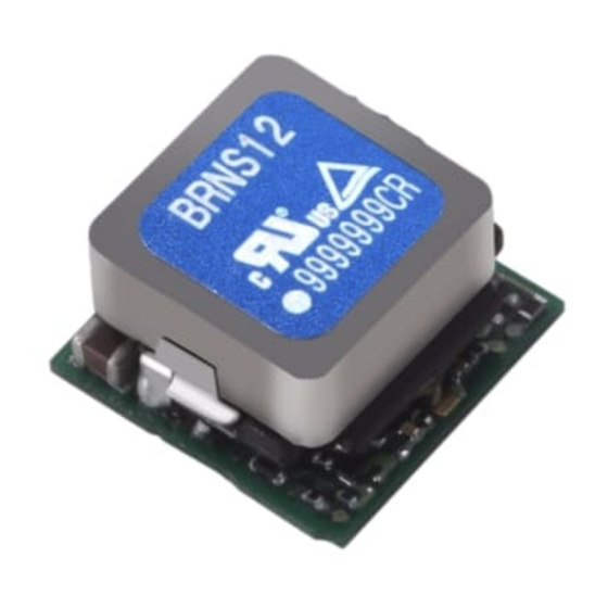
Applications manual For BRNS series 2.1 Pin configuration 1. Pin configuration Fig. 1.1 Pin connection for BRNS (bottom view) (a) BRNS6/12 (b) BRNS20 Table 1.1 Pin connection and function of BRNS BRNS 1-1... -
Page 4: Mounting And Storage
Applications manual For BRNS series 2.1 Pin configuration 2. Mounting and storage 2.1 Mounting The unit can be mounted in any direction. When two or more power supplies are used side ■ by side, position them with proper intervals to allow enough air ventilation. The temperature around each power supply should not exceed the temperature range shown in derating curve. -
Page 5: Automatic Mounting
Applications manual For BRNS series 2.2 Automatic Mounting To mount BRNS series automatically, use the coil area near the center of the PCB as ■ an adsorption point. Please see Fig.2.2.1 for details of the adsorption point. Fig. 2.2.1 Adsorption area (a) BRNS6/12 (b) BRNS20 2.3 Soldering... -
Page 6: Stencil Openings
Applications manual For BRNS series 2.4 Stencil Openings Recommended size for stencil openings is shown in Fig.2.4.1. ■ Fig. 2.4.1 Recommended size for stencil openings (Top view) (a) BRNS6 / 12 (b) BRNS20 Dimensions in mm , [ ] = inches Recommended stencil thickness is 0.12mm BRNS 2-3... -
Page 7: Cleaning
Applications manual For BRNS series 2.5 Cleaning When cleaning is necessary, clean under the following conditions. ■ : Varnishing, ultrasonic wave and vapor Method Cleaning agents : IPA (Solvent type) : 2 minutes or less Total time Do not apply pressure to the lead and name plate with a brush or scratch it during the ■... -
Page 8: Connection And Wiring
Applications manual For BRNS series 2.1 Pin configuration 3. Connection and wiring 3.1 Connection for standard use In order to use power supply, it is necessary to wire as shown in Fig. 3.1.1. ■ Fig. 3.1.1 Connection for standard use Short the following pins to turn on the power supply. -
Page 9: Wiring Input Pin
Applications manual For BRNS series 3.2 Wiring input pin (1) External fuse Fuse is not built-in on input side. In order to protect the unit, install the normal-blow ■ type fuse on input side. When the input voltage from a front end unit is supplied to multiple units, install the ■... - Page 10 Applications manual For BRNS series (4) Reverse input voltage protection Avoid the reverse polarity input voltage. It will damage the power supply. ■ It is possible to protect the unit from the reverse input voltage by installing an external diode as shown in Fig.3.2.2. Fig.
-
Page 11: Wiring Output Pin
Applications manual For BRNS series 3.3 Wiring output pin When the BRNS series supplies the pulse current for the pulse load, please install a ■ capacitor Co between +VOUT and GND pins. Fig. 3.3.1 Wiring external output capacitor Model Recommended Co Max Co Table 3.3.1 Recommended... -
Page 12: Applications Data
Applications manual For BRNS series 2.1 Pin configuration 4. Applications data 4.1 Efficiency Fig. 4.1.1 Efficiency (BRNS6) at 25℃ Input Volt. Input Volt. Input Volt. Input Volt. Input Volt. 14.4V Input Volt. 14.4V Load Current [A] Load Current [A] Vout = 1.2V Vout = 3.3V Input Volt. - Page 13 Applications manual For BRNS series Input Volt. 6.5V Input Volt. Input Volt. 14.4V Load Current [A] Vout = 5.0V Fig. 4.1.3 Efficiency (BRNS20) at 25℃ Input Volt. Input Volt. Input Volt. Input Volt. Input Volt. 14.4V Input Volt. 14.4V Load Current [A] Load Current [A] Vout = 1.2V Vout = 3.3V...
-
Page 14: Dynamic Load Response
Applications manual For BRNS series 4.2 Dynamic Load Response 4.2.1 BRNS6 Vin 12V, Vout 1.2V, Cin 22μF × 2, Cout 1000μF Testing Circuitry Fig .4.2.3.2 Cycle t1,t2=50 μs Fig. 4.2.1.1 Dynamic Load Load Current Response Load 0% (0A) ← → Load 50% (3A) 100 mV/div 100 μs/div... - Page 15 Applications manual For BRNS series 4.2.2 BRNS12 Vin 12V, Vout 1.2V, Cin 22μF × 2, Cout 1000μF Testing Circuitry Fig. 4.2.3.2 Cycle t1,t2=50 μs Fig. 4.2.2.1 Dynamic Load Load Current Response ← → Load 0% (0A) Load 50% (6A) 100 mV/div 100 μs/div 100 μs/div Load 50% ( 6 A ) ←...
- Page 16 Applications manual For BRNS series 4.2.3 BRNS20 Vin 12V, Vout 1.2V, Cin 22μF × 3, Cout 1000μF Testing Circuitry Fig. 4.2.3.2 Cycle t1,t2=50 μs Fig. 4.2.3.1 Dynamic Load Load Current Response Load 0% (0A) ← → Load 50% (10A) 100 mV/div 100 μs/div 100 μs/div Load 50% (10 A) ←...
- Page 17 Applications manual For BRNS series Fig. 4.2.3.2 Oscilloscope Bw:20MHz Measuring method of Dynamic Load Response +VIN +VOUT Cout1 Cout2 Load Input 25mm Model Cout1 Cout2 BRNS6 22μF×2 100μF 900μF BRNS12 22μF×2 100μF 900μF BRNS20 22μF×3 100μF 900μF BRNS 4-6...
-
Page 18: Ripple Voltage
Applications manual For BRNS series 4.3 Ripple Voltage Fig. 4.3.1 Ripple Voltage of BRNS at 25℃ 5 mV/div 5 mV/div Vin 12V Vout1.2V Vin 12V Vout1.2V 1 μs/div 1 μs/div Load Current 12A Load Current 6A (b) BRNS12 (a) BRNS6 10 mV/div 1 μs/div Vin 12V... -
Page 19: Rise Time
Applications manual For BRNS series 4.4 Rise time Load current:0A, Cin:22μF×2, Cout:47μF+100μF Fig. 4.4.1 BRNS6 Rise at 25℃ 200mV/div 2V/div 5ms/div 5ms/div Rise time: 3.3ms Rise time: 3.8ms Vin:8V, Vout:0.6V Vin:12V, Vout:5.5V Load current:0A, Cin:22μF×2, Cout:100μF+47μF Fig. 4.4.2 BRNS12 Rise at 25℃ 200mV/div 2V/div 5ms/div... - Page 20 Applications manual For BRNS series 4.5 Derating Shows the temperature measurement points in Figure 4.5.2 and Figure 4.5.3. ■ That the temperature of the specified point be less than or equal to the temperature shown in FIG. 1.Ambient temperature must be maintained at 85 ℃ or less. Fig.
- Page 21 Applications manual For BRNS series Fig.4.5.5 ~ 4.5.13 show the derating curve in the condition that is measured ■ as shown in Fig.4.5.4. Verify final design by actual temperature measurement. The temperature measurement location as shown in Fig.4.5.2 and Fig.4.5.3 must keep below 120℃...
- Page 22 Applications manual For BRNS series ① ② Fig. 4.5.7 Derating curve for BRNS6 at 12Vin 5.5Vout ① 1m/s ② 2m/s Ambient temperature [ ℃ ] ② Fig. 4.5.8 ① Derating curve for BRNS12 at 12Vin 1.2Vout ① 1m/s ② 2m/s Ambient temperature [ ℃...
- Page 23 Applications manual For BRNS series ① ② Fig. 4.5.11 Derating curve for BRNS20 at 12Vin 1.2Vout ① 1m/s ② 2m/s Ambient temperature [ ℃ ] ① ② Fig. 4.5.12 Derating curve for BRNS20 at 12Vin 3.3Vout ① 1m/s ② 2m/s Ambient temperature [ ℃...
- Page 24 Applications manual For BRNS series 2.1 Pin configuration 5. Adjustable voltage range Output voltage is adjustable by the external resistor. ■ The temperature coefficient could become worse, depending on the type of a resistor. ■ Resistor・・・・Metal film type, coefficient of less than ±100ppm/℃ When TRM is opened, output voltage is 0.6V.
- Page 25 Applications manual For BRNS series Please use the output voltage in the operating area of Fig.5.1.3. ■ Transient response may worsen when used in vicinity of the border of the operating area. Only for output voltage is rising and output current is small, there is a possibility that the ripple voltage is high value.
- Page 26 Applications manual For BRNS series 6. Protect circuit 2.1 Pin configuration 6.1 Overcurrent Protection Over Current Protection (OCP) is built-in and works at 105% of the rated current or higher. ■ However, use in an overcurrent situation must be avoided whenever possible. The output voltage of the power module will recover automatically when the fault causing overcurrent is corrected.
- Page 27 Applications manual For BRNS series 2.1 Pin configuration 7. Remote ON/OFF The remote ON/OFF function is incorporate in the input circuitry and operated with RC and GND. ■ If positive logic control is required , order the power supply with "-R" option. When remote on/off function is not used, please open RC.
- Page 28 Applications manual For BRNS series 2.1 Pin configuration 8. Remote sensing 8.1 When the remote sensing function is not use Fig. 8.1.1 Connection when the remote sensing is not in use When the remote sensing function is not in use, it is necessary to confirm that pins ■...
- Page 29 Applications manual For BRNS series 9.Power Good By using PGOOD, it is possible to monitor power supply whether normal ■ operation or abnormal operation. PGOOD terminal inside is comprised of at open drain. ■ Sink current of PGOOD is 50μA. Voltage of PGOOD pin become low when over current protection circuitry is work, ■...
- Page 30 Applications manual For BRNS series 10. Sequence The adjustment of the rise time is possible by connecting C ■ SEQ [nF] = 6×T [ms] - 15 RISE should be less than 1.0μF. ■ At the time of start, the output voltage follows the SEQ voltage. ■...
- Page 31 Applications manual For BRNS series With the voltage to input into SEQ pin, you can control a start sequence of plural BRNS. ■ Fig.10.1.1 Example of sequence control (a) The same time (b) The same voltage (c) The time lag If this function is unnecessary , please make SEQ pin open .
- Page 32 Applications manual For BRNS series 11. Frequency synchronization BRNS can operate at the switching frequency that synchronized to frequency of square wave ■ input into SYNC pin. There is a delay of 300nsec. Fig.11.1.1 is example of frequency synchronization. And recommended wave form of SYNC pin ■...
- Page 33 Applications manual For BRNS series As shown in Fig.11.1.3, frequency synchronization is possible without using an outside clock. ■ Fig. 11.1.3 Example of CLK pin connection The maximum synchronization number is 5. ■ After the power supply which output CLK started, please start the synchronizing power supplies. ■...
- Page 34 Applications manual For BRNS series 12. Series operation/Parallel operation/Redundancy operation 12.1 Series operation Series operation is not possible. ■ 12.2 Parallel operation/Redundancy operation Parallel operation is not possible. ■ Redundancy operation is available by wiring as shown below. ■ Fig. 12.2.1 Redundancy operation Even a slight difference in output voltage can affect the balance between ■...
- Page 35 Applications manual For BRNS series 2.1 Pin configuration 13. Package Information Please refer to Fig.13.1.1 ~ Fig.13.1.3 for Package form ( Reel ). ■ The packed number is 200. ■ Fig. 13.1.1 Taping dimensions of BRNS6/12 Fig. 13.1.2 Taping dimensions of BRNS20 BRNS 13-1...
- Page 36 Applications manual For BRNS series Fig. 13.1.3 Reel dimensions of BRNS BRNS 13-2...
- Page 37 Applications Manual BRFS/BRDS series Page 1. Pin configuration BRFS/BRDS 1-1 BRFS30/40 BRFS/BRDS 1-1 BRFS50/BRFS50L/BRFS60/BRFS100 BRFS/BRDS 1-2 BRDS40 BRFS/BRDS 1-3 BRDS60/100 BRFS/BRDS 1-4 2. Mounting and storage BRFS/BRDS 2-1 Mounting BRFS/BRDS 2-1 Automatic mounting BRFS/BRDS 2-3 Soldering BRFS/BRDS 2-4 Cleaning BRFS/BRDS 2-5...
-
Page 38: Pin Configuration
Applications manual For BRFS/BRDS series 2.1 Pin configuration 1. Pin configuration 1.1 BRFS30/40 Fig.1.1.1 Pin connection for BRFS30/40/60S (bottom view) Table.1.1.1 Pin connection and function of BRFS30/40/60S BRFS/BRDS 1-1... - Page 39 Applications manual For BRFS/BRDS series 1.2 BRFS50/50L/60/100/120/150 Fig.1.2.1 Pin connection for BRFS50/50L/60/100 /120/150 (bottom view) (a) BRFS50/50L/60/120 (b) BRFS100/150 Table.1.2.1 Pin connection and function of BRFS50/ 50L/60/100/120/150 BRFS/BRDS 1-2...
-
Page 40: Brds40
Applications manual For BRFS/BRDS series 1.3 BRDS40 Fig.13.1 Pin connection for BRDS40/60S (bottom view) Table.13.1 Pin connection and function of BRDS40/60S BRFS/BRDS 1-3... - Page 41 Applications manual For BRFS/BRDS series 1.4 BRDS60/100 Fig.1.4.1 Pin connection for BRDS60/100/120 (bottom view) (a) BRDS60/120 (b) BRDS100/150 Table.1.4.1 Pin connection and function of BRDS60/100 /120/150 BRFS/BRDS 1-4...
-
Page 42: Mounting And Storage
Applications manual For BRFS/BRDS series 2.1 Pin configuration 2. Mounting and storage 2.1 Mounting The unit can be mounted in any direction. When two or more power supplies are used side by ■ side, position them with proper intervals to allow enough air ventilation. The temperature around each power supply should not exceed the temperature range shown in derating curve. - Page 43 Applications manual For BRFS/BRDS series (c-1)BRFS40/60S (c-2)BRDS40/60S (d-1)BRFS100/150 (d-2)BRDS100/150 BRFS/BRDS 2-2...
-
Page 44: Automatic Mounting
Applications manual For BRFS/BRDS series 2.2 Automatic Mounting To mount BRFS/BRDS series automatically, use the coil area near the center of the ■ PCB as an adsorption point. Please see Fig.2.2.1 for details of the adsorption point. Fig.2.2.1 Adsorption area... -
Page 45: Soldering
Applications manual For BRFS/BRDS series 2.3 Soldering Fig.2.3.1 shows condition for reflow of BRFS/BRDS series. Please make sure that the ■ temperature of pin shown in Fig.2.3.2 do not exceed the temperatures shown in Fig.2.3.1 While soldering, having vibration or impact on the unit should beavoided, because of ■... -
Page 46: Cleaning
Applications manual For BRFS/BRDS series 2.4 Cleaning When cleaning is necessary, clean under the following conditions. ■ : Varnishing, ultrasonic wave and vapor Method Cleaning agents : IPA (Solvent type) : 2 minutes or less Total time Do not apply pressure to the lead and name plate with a brush or scratch it during the ■... -
Page 47: Connection For Standard Use
Connect resistance to set the output voltage between TRM and GND. ■ Between input and output is not isolated . ■ The BRFS/BRDS series handle only the DC input. ■ Avoid applying AC input directly. It will damaged the power supply. -
Page 48: Wiring Input Pin
Applications manual For BRFS/BRDS series 3.2 Wiring input pin (1) External fuse Fuse is not built-in on input side. In order to protect the unit, install the normal-blow ■ type fuse on input side.(Recommended fuse current shown by Table3.2.1) When the input voltage from a front end unit is supplied to multiple units, install the ■... - Page 49 Applications manual For BRFS/BRDS series (4) Reverse input voltage protection Avoid the reverse polarity input voltage. It will damage the power supply. ■ It is possible to protect the unit from the reverse input voltage by installing an external diode as shown in Fig.3.2.2.
-
Page 50: Wiring Output Pin
Applications manual For BRFS/BRDS series 3.3 Wiring output pin When the BRFS/BRDS series supplies the pulse current for the pulse load, ■ please install a capacitor Co between +VOUT and GND pins. Fig.3.3.1 Wiring external output capacitor Model Recommend Co Maximum Co Table.3.3.1... - Page 51 Applications manual For BRFS/BRDS series The inductance reduction of output line, it can reduce the fluctuation of the ■ power supply output voltage. Inductance must not be inserted ■ Lowering the inductance of the board pattern ■ No inductance Fig.3.3.3...
-
Page 52: Efficiency
Applications manual For BRFS/BRDS series 4. Overview 2.1 Pin configuration 2.1 Pin configuration 4.1 Efficiency Fig 4.1.1 Efficiency (BRFS30) at 25℃ Input Volt. 4.5V Input Volt. 4.5V Input Volt. Input Volt. Input Volt. Input Volt. Load Current [A] Load Current [A] Vout = 0.8V... - Page 53 Applications manual For BRFS/BRDS series Fig 4.1.2 Efficiency (BRFS40/BRDS40) at 25℃ Input Volt. 4.5V Input Volt. 4.5V Input Volt. Input Volt. Input Volt. Input Volt. Load Current [A] Load Current [A] Vout = 0.6V Vout = 1.0V Input Volt. 4.5V Input Volt.
- Page 54 Applications manual For BRFS/BRDS series Fig 4.1.3 Efficiency (BRFS50) at 25℃ Input Volt. 4.5V Input Volt. 4.5V Input Volt. Input Volt. Input Volt. Input Volt. Load Current [A] Load Current [A] Vout = 0.7V Vout = 1.0V Input Volt. 4.5V Input Volt.
- Page 55 Applications manual For BRFS/BRDS series Fig 4.1.4 Efficiency (BRFS60/BRDS60) at 25℃ Input Volt. 4.5V Input Volt. 4.5V Input Volt. Input Volt. Input Volt. Input Volt. Load Current [A] Load Current [A] Vout = 0.7V Vout = 1.0V Input Volt. 4.5V Input Volt.
- Page 56 Applications manual For BRFS/BRDS series Fig 4.1.5 Efficiency (BRFS100/BRDS100) at 25℃ Input Volt. 4.5V Input Volt. 4.5V Input Volt. Input Volt. Input Volt. Input Volt. Load Current [A] Load Current [A] Vout = 0.7V Vout = 1.0V Input Volt. 4.5V Input Volt.
- Page 57 Applications manual For BRFS/BRDS series Fig 4.1.6 Efficiency (BRFS60S/BRDS60S) at 25℃ Input Volt. 4.5V Input Volt. 4.5V Input Volt. 4.5V Input Volt. Input Volt. Input Volt. Input Volt. Input Volt. Input Volt. Vout = 0.6V Vout = 1.0V Input Volt.
- Page 58 Applications manual For BRFS/BRDS series Fig 4.1.7 Efficiency (BRFS120/BRDS120) at 25℃ Input Volt. 4.5V Input Volt. 4.5V Input Volt. Input Volt. Input Volt. Input Volt. Vout = 0.6V Vout = 1.0V Input Volt. 4.5V Input Volt. 4.5V Input Volt. Input Volt.
- Page 59 Applications manual For BRFS/BRDS series Fig 4.1.8 Efficiency (BRFS150/BRDS150) at 25℃ Input Volt. 4.5V Input Volt. 4.5V Input Volt. Input Volt. Input Volt. Input Volt. Vout = 0.6V Vout = 1.0V Input Volt. 4.5V Input Volt. 4.5V Input Volt. Input Volt.
- Page 60 Applications manual For BRFS/BRDS series 4.2 Dynamic Load Response 4.2.1 Wave Form 1)BRFS30 Vin 12V, Vout 1.2V, Cin 22μF × 4, Cout 4000μF Testing Circuitry Fig.4.2.3.1 Cycle 5 m t1,t2=50 μs Fig.4.2.1.1 Load Current Dynamic Load Response Min. Load (0A) ←→...
- Page 61 Applications manual For BRFS/BRDS series 2)BRFS40 , BRDS40 Vin 12V, Vout 1.2V Cin 22μF × 4, Cout 4000μF Testing Circuitry Fig 4.2.3.1 Fig 4.2.1.2 Cycle t1,t2=50 μ s Dynamic Load Load Current Response Min. Load (0 A) ← → Load 50% (20A) 100 mV/div 100 μs/div...
- Page 62 Applications manual For BRFS/BRDS series 3)BRFS50 Vin 12V, Vout 1.2V, Cin 22μF × 4, Cout 4000μF Testing Circuitry Fig.4.2.3.1 Cycle t1,t2=50 μs Fig.4.2.1.3 Dynamic Load Load Current Response Min. Load (0 A) ← → Load 50% (25A) 100 mV/div 100 μs/div 100 μs/div...
- Page 63 Applications manual For BRFS/BRDS series 4) BRFS60,BRDS60 Vin 12V, Vout 1.2V, Cin 22μF × 4, Cout 4000μF Testing Circuitry Fig.4.2.3.1 Cycle t1,t2=50 μ s Fig.4.2.1.4 Dynamic Load Load Current Response Min. Load (0 A) ← → Load 50% (30A) 100 mV/div 100 μs/div...
- Page 64 Applications manual For BRFS/BRDS series 5)BRFS100,BRDS100 Vin 12V, Vout 1.2V, Cin 22μF × 4, Cout 8000μF Testing Circuitry Fig.4.2.3.1 Cycle t1,t2=50 μ s Fig.4.2.1.5 Dynamic Load Load Current Response Min. Load (0 A) ← → Load 50% (50A) 100 mV/div 100 μs/div...
- Page 65 Applications manual For BRFS/BRDS series 6)BRFS60S,BRDS60S Vin 12V, Vout 1.2V, Cin 22μF × 4, Cout 4000μF Testing Circuitry Fig.4.2.3.2 Cycle t1,t2=50 μ s Fig.4.2.1.6 Dynamic Load Load Current Response Min. Load (0 A) ← → Load 50% (30A) 100 mV/div 100 μs/div...
- Page 66 Applications manual For BRFS/BRDS series 7)BRFS120,BRDS120 Vin 12V, Vout 1.2V, Cin 22μF × 2, Cout 4000μF Testing Circuitry Fig.4.2.3.2 Cycle t1,t2=50 μ s Fig.4.2.1.7 Dynamic Load Load Current Response Min. Load (0 A) ← → Load 50% (60A) 100 mV/div 100 μs/div...
- Page 67 Applications manual For BRFS/BRDS series 8)BRFS150,BRDS150 Vin 12V, Vout 1.2V, Cin 22μF × 2, Cout 4000μF Testing Circuitry Fig.4.2.3.2 Cycle t1,t2=50 μ s Fig.4.2.1.8 Dynamic Load Load Current Response Min. Load (0 A) ← → Load 50% (75A) 100 mV/div 100 μs/div...
- Page 68 Applications manual For BRFS/BRDS series 4.2.2 Capacitance ‐ Dynamic Load Response characteristics 1)BRFS30 Vin 12V, Cin 22μF × 4, SR 1A/μs, Testing Circuitry Fig.4.2.3.1 Fig.4.2.2.1 0-50% Vout=0.8V Capacitance ‐ 0-50% Vout=1.2V Dynamic Load 0-50% Vout=3.3V Response characteristics (BRFS30) 1000 2000...
- Page 69 Applications manual For BRFS/BRDS series Vin 12V, Cin 22μF × 4, SR 1A/μs, Testing Circuitry Fig.4.2.3.2 3)BRFS50 Fig 4.2.2.3 Capacitance ‐ 0-80% Vout=0.7V Dynamic Load 0-80% Vout=1.2V Response 0-80% Vout=2V characteristics (BRFS50) 1000 2000 3000 4000 Cout(μF) ⊿ V ⊿...
- Page 70 Applications manual For BRFS/BRDS series 5) BRFS100/BRDS100 Vin 12V, Cin 22μF × 4, SR 1A/μs, Testing Circuitry Fig.4.2.3.1 Fig 4.2.2.5 0-50% Vout=0.7V Capacitance ‐ 0-50% Vout=1.2V Dynamic Load 0-50% Vout=2.0V Response characteristics (BRFS100/BRDS100) 2000 4000 6000 8000 Cout(μF) ⊿ V ⊿...
- Page 71 Applications manual For BRFS/BRDS series 7) BRFS120/BRDS120 Vin 12V, Cin 22μF × 2, SR 1A/μs, Testing Circuitry Fig.4.2.3.2 Fig 4.2.2.7 Capacitance ‐ Dynamic Load Response characteristics (BRFS120/BRDS120) ⊿ V ⊿ ⊿ V= ⊿ V ( ⊿ V > ⊿ V or ⊿...
- Page 72 Applications manual For BRFS/BRDS series 4.2.3 Figure Fig.4.2.3.1 Measuring method Oscilloscope Bw:20MHz of Dynamic Load Response +VOUT +VIN Cout Input Load Model BRFS30 10mm BRFS40/100 ・ BRDS40/100 50mm Fig.4.2.3.2 Measuring method Oscilloscope Bw:20MHz of Dynamic Load Response +VOUT +VIN Cout Input Load Model BRFS50/60/60S/120/150 ・...
- Page 73 Applications manual For BRFS/BRDS series 4.3 Ripple Voltage Fig.4.3.1 Ripple Voltage of BRFS/BRDS 10 mV/div 10 mV/div 2 μs/div 2 μs/div Vin 12V,Vout1.2V, Load Cuurent 30A Vin 12V,Vout1.2V, Load Cuurent 40A Cin 22μF × 4 , Cout 100μF × 3 Cin 22μF ×...
- Page 74 Applications manual For BRFS/BRDS series 10 mV/div 10 mV/div 2 μs/div 2 μs/div Vin 12V,Vout1.2V, Load Cuurent 120A Vin 12V,Vout1.2V, Load Cuurent 150A Cin 22μF × 2 , Cout 100μF × 4 Cin 22μF × 2 , Cout 100μF × 4...
- Page 75 Applications manual For BRFS/BRDS series 4.4 Rise time Vin : 12V , Load current:0A , Cin:22uFx4 Fig. 4.4.1 BRFS30 Cout:300uF 500mV/div 1V/div 5ms/div 5ms/div Rise time: 1.0ms Rise time: 5.5ms (a) Vout : 0.8V (b) Vout : 3.63V Fig. 4.4.2...
- Page 76 Applications manual For BRFS/BRDS series Fig. 4.4.5 BRFS100,BRDS100 Cout:400uF 200mV/div 1V/div 5ms/div 5ms/div Rise time: 1.0ms Rise time: 3.0ms (a) Vout : 0.7V (b) Vout : 2.0V Fig. 4.4.6 BRFS60S,BRDS60S Cout:400uF 200mV/div 1V/div 5ms/div 5ms/div Rise time: 1.0ms Rise time: 3.5ms (a) Vout : 0.6V...
- Page 77 Applications manual For BRFS/BRDS series 4.5 Derating Make sure the temperatures measurement locations shown from Fig.4.5.2 and Fig.4.5.3 ■ below are on or under the derating curve in Fig.4.5.1. Ambient temperature must be kept at 85℃ or under. Fig.4.5.1 Derating curve for BRFS Fig.4.5.2...
- Page 78 Applications manual For BRFS/BRDS series Fig.4.5.5 ~ 4.5.10 show the derating curve in the condition that is measured ■ as shown in Fig.4.5.4. Verify final design by actual temperature measurement. The temperature measurement location as shown in Fig.4.5.2 and Fig.4.5.3 must keep below 120 ℃.
- Page 79 Applications manual For BRFS/BRDS series Fig.4.5.7 ② Derating curve ① for BRFS30 at 12Vin 3.3Vout ① 1m/s ② 2m/s Ambient temperature [℃] ② Fig.4.5.8 Derating curve for BRFS50 ① at 12Vin 0.7Vout ① 1m/s ② 2m/s Ambient temperature [℃] ②...
- Page 80 Applications manual For BRFS/BRDS series ② Fig.4.5.8 Derating curve for BRFS40/BRDS40 ① at 12Vin 0.7Vout ① 1m/s ② 2m/s Ambient temperature [℃] Ambient temperature [℃] Fig.4.5.9 ② Derating curve for BRFS40/BRDS40 ① at 12Vin 1.2Vout ① 1m/s ② 2m/s Ambient temperature [℃] Fig.4.5.10...
- Page 81 Applications manual For BRFS/BRDS series Fig.4.5.8 ② Derating curve for BRFS60/BRDS60 ① at 12Vin 0.7Vout ① 1m/s ② 2m/s Ambient temperature [℃] Fig.4.5.9 ② Derating curve for BRFS60/BRDS60 at 12Vin 1.2Vout ① ① 1m/s ② 2m/s Ambient temperature [℃] Fig.4.5.10 ②...
- Page 82 Applications manual For BRFS/BRDS series Fig.4.5.8 ② Derating curve for BRFS100/BRDS100 at 12Vin 0.7Vout ① ① 1m/s ② 2m/s Ambient temperature [℃] Fig.4.5.9 Derating curve ② for BRFS100/BRDS100 at 12Vin 1.2Vout ① ① 1m/s ② 2m/s Ambient temperature [℃] Fig.4.5.10 Derating curve ②...
- Page 83 Applications manual For BRFS/BRDS series Fig.4.5.11 ② Derating curve for BRFS60S/BRDS60S ① at 12Vin 0.6Vout ①1m/s ②2m/s Ambient temperature [℃] Fig.4.5.12 Derating curve ② for BRFS60S/BRDS60S at 12Vin 1.2Vout ① ① 1m/s ② 2m/s Ambient temperature [℃] Fig.4.5.13 ② Derating curve for BRFS60S/BRDS60S at 12Vin 2.0Vout...
- Page 84 Applications manual For BRFS/BRDS series Fig.4.5.14 Derating curve ② for BRFS120/BRDS120 at 12Vin 0.6Vout ① ① 1m/s ② 2m/s Ambient temperature [℃] Fig.4.5.15 Derating curve ② for BRFS120/BRDS120 at 12Vin 1.2Vout ① ① 1m/s ② 2m/s Ambient temperature [℃] Fig.4.5.16...
- Page 85 Applications manual For BRFS/BRDS series Fig.4.5.17 Derating curve ② for BRFS150/BRDS150 at 12Vin 0.6Vout ① ① 1m/s ② 2m/s Ambient temperature [℃] Fig.4.5.18 Derating curve for BRFS150/BRDS150 ② at 12Vin 1.2Vout ① ① 1m/s ② 2m/s Ambient temperature [℃] Fig.4.5.19...
- Page 86 Applications manual For BRFS/BRDS series 4.6 Thermal simulation model We offers a thermal simulation model that can be used for thermal design. ■ It shows the simulation model and the simulation example of BRFS30 and BRFS50 below. These model will enable thermal design on simulation using ANSYS icepack.
- Page 87 Applications manual For BRFS/BRDS series 2.1 Pin configuration 5. Adjustable voltage range Output voltage is adjustable by the external resistor. ■ The temperature coefficient could become worse, depending on the type of a resistor. ■ Resistor・・・・Metal film type, coefficient of less than ±100ppm/℃...
- Page 88 Applications manual For BRFS/BRDS series 2.1 Pin configuration 6. Protect circuit 6.1 Overcurrent Protection Over Current Protection (OCP) is built-in and works at 105% of the rated current or higher. ■ However, use in an overcurrent situation must be avoided whenever possible.
- Page 89 Applications manual For BRFS/BRDS series 2.1 Pin configuration 7. Remote ON/OFF The remote ON/OFF function is incorporate in the input circuitry and operated with RC and -Vin. ■ If positive logic control is required , order the power supply with "-R" option.
- Page 90 Applications manual For BRFS/BRDS series 8. Remote sensing 2.1 Pin configuration 8.1 When the remote sensing function is not in use Fig. 8.1.1 Connection when the remote sensing is not in use When the remote sensing function is not in use, it is necessary to confirm that pins ■...
- Page 91 Applications manual For BRFS/BRDS series 9.Power Good Power Good is built-in, internal circuitry as shown in Fig.9.1.1. ■ Power Good pin becomes low state(0.3V max), when output becomes condition ■ such as overcurrent or output voltage ±12.5%(Typ) outside the set point value.
- Page 92 Applications manual For BRFS/BRDS series 10. Series operation / Parallel operation 10.1 Series operation Series operation is not possible. ■ 10.2 Parallel operation 1)The basic note Parallel operation is not possible BRFS30/40/60S ■ *1 BRFS40/60S has a parallel option "P". Parallel operation is impossible different series.
- Page 93 Applications manual For BRFS/BRDS series 3)Patterning of the PCB Input and output pattern should be the same width and length. ■ Voltage drop from the output terminal to remote sensing point must be less than 0.2V. ■ ESR from the slave of the output terminal to remote sensing point must be 10mΩ or less ■...
- Page 94 Applications manual For BRFS/BRDS series 11. Sequence The adjustment of the rise time is possible by connecting C ■ Fig.11.1.1 Example of soft start circuitry When the voltage is applied to the terminal SEQ , the output voltage tracks this voltage ■...
- Page 95 Applications manual For BRFS/BRDS series With the voltage to input into SEQ pin , you can control a start sequence of plural BRFS/BRDS . ■ Fig.11.1.4 (a) The same Example of time sequence control (a) The same (b) The same voltage...
- Page 96 Applications manual For BRFS/BRDS series 2.1 Pin configuration 12. Package Information Please refer to Fig.12.1.1 ~ Fig.12.1.3 for Package form ( Reel ). ■ The packed number is shown in Table 12. ■ Table.12.1.1 Model Capacity of reel Packed number BRFS30/40 ・...
- Page 97 Applications manual For BRFS/BRDS series Fig 12.1.3 Taping dimensions of BRFS100/150・ BRDS100/150 Fig 12.1.3 Reel dimensions of BRFS/BRDS BRFS/BRDS 12-2...
- Page 98 Applications Manual CHS series and BR series Page 1. Power Supply of Cosel for Intermediate Bus Architecture CHS and BR 1-1 2. Applications data CHS and BR 2-1 2.1 Startup Sequence CHS and BR 2-1 2.2 Efficiency of the combination of CHS and BR CHS and BR 2-2 2.3 Dynamic Input Response...
-
Page 99: Power Supply Of Cosel For Intermediate Bus Architecture
Applications manual For CHS series and BR series 2.1 Pin configuration 1. Power Supply of Cosel for Intermediate Bus Architecture (Bus Converter) (Point of load) Fig.1.1.1 Intermediate Bus 1.0V Architecture Core Isolated OBP FPGA 3.3V optical module CHS series BR series ●... - Page 100 Applications manual For CHS series and BR series 2.1 Pin configuration 2. Applications data 2.1 Startup Sequence 2.1.1 CHS4004812 and BRNS20 Fig.2.1.1 Startup Sequence of CHS Vout CHS Vout (10V/div) (10V/div) CHS4004812 and BRNS20 BRNS Vout BRNS Vout (1V/div) (1V/div) BRNS Iin BRNS Iin (5A/div)
-
Page 101: Chs And Br
Applications manual For CHS series and BR series 2.2 Efficiency of the combination of CHS and BR When used in a 10V bus voltage, the efficiency of the device is higher than the bus ■ voltage 12V. When using CHS300/4004812H, the efficiency of the device is higher than using ■... -
Page 102: Chs And Br
Applications manual For CHS series and BR series Fig.2.2.3 The efficiency of CHS300/400 at 25℃ CHS4004810 CHS3004810 CHS4004812 CHS3004812 CHS4004812H CHS3004812H Load Current [A] Load Current [A] (b) Efficiency (CHS400) (a) Efficiency (CHS300) CHS400 Vin=48V CHS300 Vin=48V Fig.2.2.4 The efficiency of BRNS20/BRFS50 at 25℃... -
Page 103: Chs And Br
Applications manual For CHS series and BR series 2.3 Dynamic Input Response 2.3.1 CHS4004812 and BRNS20 Fig.2.3.1 CHS Iout CHS Iout Dynamic Input Response of CHS4004812 BRNS Vin BRNS Vin and BRNS20 (CHS Vout) (CHS Vout) (500mV/div) (500mV/div) BRNS Vout BRNS Vout (50mV/div) (50mV/div)
Need help?
Do you have a question about the BRDS series and is the answer not in the manual?
Questions and answers