Table of Contents
Advertisement
Quick Links
Advertisement
Table of Contents

Related Manuals for FLY IQ442 QUAD


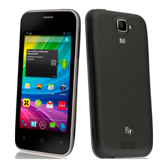
Summary of Contents for FLY IQ442 QUAD
- Page 1 .+TIANYU CONFIDENTIAL Maintenance Work Guide for IQ442 QUAD...
-
Page 2: Introduction
The readers of the document should be the debug worker of SMT and after-service. It will be the work guide for them. At the same time, the other members of the IQ442 QUAD project group can also refer to the documents. -
Page 3: Table Of Contents
INTRODUCTION ..........................2 1、System summary ......................... 4 1.1 The diagram of IQ442 QUAD: ................... 4 1.2 The main components list: ....................5 2 The details of system model ......................6 2.1 Radio model ........................6 2.1.1 The radio Transceiver ....................6 2.1.2 GSM signal’s path ..................... -
Page 4: 1、System Summary
1、System summary 1.1 The diagram of IQ442 QUAD: The below is the diagram of IQ442 QUAD, which consist of main function blocks for the phone. It can help find the root cause for different issues. Diagram 1.1 The function block The mobile consists of below main parts: 1. -
Page 5: The Main Components List
It concludes the peripheral parts of mobile, USB,BT, WIFI,GPS, T-flash, Dual SIM-card, g-sensor, LCM, Touch panel, front and back camera, light sensor, etc. 1.2 The main components list: IQ442 QUAD hardware board consists of main board、 sub-board、 front-camera FPCA and on-key FPC. the main board parts list: ... -
Page 6: The Details Of System Model
U1401:The flash LED U1801,U1803:GPS saw filter U1802:GPS LNA U501: audio amplifier J5460:the volume down/up key J5351:headset socket 2 The details of system model U101 is the AP+BP CPU, U202 is the AP&BP memory, the system can power up while they are working normally. - Page 7 Diagram 3 GSM’s high and low bands signals come out from the U1101 When GSM’s high and low bands come out from U1101, after a resistor attenuator network, input the U1204 from PIN9 and PIN10,then come out again from U1207’s PIN25 after they be amplified in it.
-
Page 8: Wcdma Signal's Path
U1101 after they through the match network. The path described above can refer to figure 6 and figure 7. Diagram 6 GSM radio RX Diagram 7 GSM RX signals into TSC (U1101) 2.1.3 WCDMA signal’s path IQ442 QUAD supports wcdma band1 and band8.They will be described as below:... - Page 9 Such above diagram showing, the WCDMA L/H band signals are output from U1101; TX_WCDMA_LB is low band signal, TX_WCDMA_HB_SE is high band signal. 1. WCDMA BAND 1 TX path: Band1’s tx signal comes from U1101, and after through some match networks and tx saw filter U1205, it arrives band1’s PA U1203, then enter in diplexer U1210, then enter the switchU1204.
-
Page 10: Power Management Unit
from U1210’s PIN1, then enter in U1101 after through C1252. BC8’s signal comes out from U1201’s PIN1and PIN8 which is a differential signal. Then it enters in U1101 after through a match network and C1201 and C1209.The path was described in figure 10 as below. Diagram 10 WCDMA BC1 and BC8 RX After BC1’s signal entered in U1101, in order to improve the SN parameter, The transceiver amplified the signal first in its internal LNA, and then puts out the BC1‘s signal. -
Page 11: Pmu Output Voltage
MOSFET—U803. 3. PMU puts out all the voltage according to the boot timing. 4. PMU pulls the pin PON_RESET_N to high level,and reset the U101. 5. After the CPU U101 reset, it pulls the PS_HOLD signal to high, in order to keep boot status. Note:If the power key was pressed up before the PS_HOLD was pulled to high, the phone will not boot normally. -
Page 12: Memory
Diagram 12 DC-DC output for CPU core2 2.3 Memory SDRAM + NAND Flash Memory save the program code and run the program. If they have some any problems, the system will not boot up or the system can’t download the system’s program code. -
Page 13: Audio Model
re-download new software. 2.5 Audio model 2.5.1 MIC U101 can provide the audio signal’s encode and decode functions for the system. So we just describe the details on the path out of the U101. The main microphone was welded on the pads printed on the antenna sub board .The microphone’s differential signal go through the sub board and FPC, and then arrival the U101 after through the filter network which can be referred to figure 14 Diagram 14 main mic... -
Page 14: Speaker
2.5.3 Speaker Speaker‘s signal come out fromU101, then be amplified by the audio PA U501, drive the speaker. After be amplified, the speaker’s signal arrival the pads on antenna sub board after through the FPC and the connector J1501. It need pay attention to U501 SMT issue, which it is bad soldering, the speaker is no sound. -
Page 15: Other Peripherals
Diagram 17 audio jack 2.6 Other peripherals 2.6.1 Vibrator VBAT is the anode; VIB_DRV_N puts out the low level to drive the vibrator to shock. VIBA_DRV-N is from U802 to J1501 and through the FPC to sub board to drive vib Diagram 18 vibrator 2.6.2 Touch panel circuit The TP is communicating with U101 through the interface IIC. -
Page 16: Camera
Diagram 19 Touch panel 2.6.3 Camera IQ442 QUAD has a front Camera and a main camera. 1. Main camera circuit Main Camera is welded on camera FPC, and the peripherals are welded on main board. The camera and main board connect together through the connector J1403. -
Page 17: Light Sensor Circuit
Diagram 21 back camera 2. Front camera The front camera is connected by FPC J1402. Diagram 22 front camera 2.6.4 Light sensor circuit Light sensor is communicate with U101 through the IIC interface... -
Page 18: G-Sensor
Diagram23 light sensor Light sensor’s failure often was caused by sealed not well or other devices shared IIC have something wrong. 2.6.5 G-sensor The G-sensor is communicated with U101 by I2C. Diagram 24 G-sensor 2.6.6 Bluetooth & WIFI module BT and WIFI module was made up of U1602、 U1604、 U1607. U1602 is the filter for BT and WIFI. The BT &... - Page 19 Diagram 26 the Bluetooth power Diagram 27 WIFI & BT ant FEM Diagram 28 WIFI model...
-
Page 20: Gps
2.6.7 GPS The GPS signal through the saw filter U1801, low noise amplifier U1802, saw filter U1803, then arrivals U1101. Diagram 29 Gps RF front 图 29 GPS 模块 RF 前端电路 Diagram 30 GPS RF to TSC Diagram 31 GPS IQ to CPU... -
Page 21: Lcd
2.6.8 LCD LCD module communicates with cpu through the MIPI_DSI interface circuit. The device U1701 is the common filter for data and clock signal of MIPI_DSI interface. Diagram 32 LCD’s interface The following diagram is the back light driver circuit. If the back light led has some problems, please check the voltage on R1723, or check the D1702 and L1720 whether or not is burn out . -
Page 22: Peripheral Interface Io
2.7 Peripheral interface IO 2.7.1 USB interface USB interface is on the antenna sub board , and communication with CPU by FPC. 2.7.2 Side key While the KYPD_DRV1 and KEYSENSE_N1 are shorted together,the volume up is pressed; while the KYPD_DRV0 and KEYSENSE_N1 are shorted together,the volume down is pressed; the up/down keys are pressed together, it is into download mode. -
Page 23: Tf Card And Usim Card Interface
2.7.3 TF Card and USIM Card interface Diagram 35 dul-sim card Diagram 36 T-flash 3. The factory happened case For the IQ442 QUAD project, there are below cases happened while producing for reference:... -
Page 24: Epilog
It needs to check the PMU short circuit. Epilog This document’s purpose is to help the after-sales staff to maintain the IQ442 QUAD mobile phone, and to provide the better after-sales service for our customer. If you want to know...
Need help?
Do you have a question about the IQ442 QUAD and is the answer not in the manual?
Questions and answers